Note: Descriptions are shown in the official language in which they were submitted.
-1-
PILL INTRRLACI~ ~PP~TT'BS 3~dD 1lD;THOD
~~»~~~3.
B~C1C(3ROU~D OF THB IIOIT
FIELD OF THE IBiTIO~T
The present invention is directed to a device for
capturing and processing image information using a pseudo
random pixel interlace. This process permits the use of
this image information by a variety of normally
incompatible interfaces.
RFLAT$p l,RT
There are four common frame rates used in moving
imagery in the world today. In the U.S. and Japan, NTSC
has a 59.94 Hz interlaced field rate. In~Europe, PAL and
SEGAM have a 50.0 Hz interlaced field rate. The motion
picture industry predominantly uses 24 frame per second
film. Some High Definition Television (HDT~1) proposals
use ~60.0 Hz interlaced fields (such as the Japanese
standard developed .by NHK, also called SMPTE 240M and BTA-
002), and some use 60.O~Hz progressively scanned images
(non-interlaced) (presently under discussion in the United
States). Thus 24, 50, 59.94, and 60.0 Hz are common
picture frame rates in the world.
On motion picture film, 30 Hz, 60 Hz, and 72 Hz have
all been used on occasion.
on computer displays, progressively scanned (non
interlaced) images are often displayed at 66 Hz (Apple
Macintosh II color screen), 7o Hz, 72 Hz, 75 Hz, and 76
Hz. These CRT screen refresh rates exceed 60 Hz because
the 60 Hz rate flickers excessively under fluorescent
lights in bright viewing environments as found in most
offices.
For covering sports, motion rates faster than 45 Hz
are felt to be required.
Further, current television formats have either 240
-z-
lines per field for NTSC or 288 lines per field for
European PAL. In other countries, such as those in South
America, other combinations of PAL and NTSC line formats
and rates are found.
With limited exceptions, these frame rates and line
formats are incompatible with each other. Fox a single
viewable event, therefore, this incompatibility makes it
necessary to have a number of different corresponding
video image capturing and formatting devices in order for
different end-viewers to be able to view the event.
Similarly, the incompatibility makes it extremely
difficult to transfer information recorded in one format
to another format.
For example, when mQVing images axe captured in the
U.S. in'iJTSC, they must be converted to European PAh for
display. in Europe, or to other formats. This conversion
process is sometimes called "transcoding". Both the field
anw frame rates, as_.rell as the number of scan lines mast
be converted. This transcoding conversion process is
usually expensive. Worse yet, the results of transcoding
are often felt to be poor, and the transcoding process is
prone to aliasing artifacts and resolution degradation, as
well as motion degradation.
As indicated above, some of the present-day systems
use interlace as part of the video format. Interlace is
a technique which is used to provide some motion at 50 or
59.94 or 60 Hz for sports coverage. However, interlace is
prone to aliasing artifacts, both temporally ( in time) and
spatially (on image details). Further, interlace makes it
difficult to perform transcoc3ings, since scan lines do not
sample the correct portions of the image as are required
for proper transcodings to other formats. Thus, a "de-
interlacer" is often used to simulate the removal of
interlace before applying transcoding. Such de-
interlacers are also prone to motion and picture detail
artifacts and image resolution degradation.
An obj ective of the present invention therefore is to
provide a format for images that is high quality and
capable of use by any presently--used or contemplated
picture rate.
Another fundamental problem of many present image
formats is that they use interlace, which is a regular
undersampling pattern. Such patterns are known in the art
to be improper theoretical image filters, and which result
in temporal and spatial artifacts through the regularity
of the sampling pattern and the interactian of this
pattern with natural patterns of detail in the image.
An object of the present invention, therefore, is to
provide a sampling-pattern that yminimizes temporal and
spatial artifacts.
Another object of the present invention is to provide
an image-format that i~.comratible with all the commonly
used picture rates, as well as those rates expected in the
future.
Moreover, any-proposed image format should be usable
by variety of displays to shave varying degrees of quality,
as appropriate for each display, from the same signal.
Thus, another objective of the present invention is
to provide a distribution signal format where a variety of
displays, at various levels of cost and performance, can
be used when receiving the signal.
Further, the present invention allows a variety of
images derived from different picture sources to be
displayed individually on the same screen, or to be
combined together for a composite image. The present
invention thus eliminates the need for complex frame
buffering normally required to provide synchronization for
such simultaneous displays of images.
_4_.
The present invention incorporates a method referred
to herein as '°pixel interlacing." The present method is
referred to as pixel interlacing since it involves the
extension of the concegt of line interlace on a pixel-by
pixel basis.
Because pixel interlacing in the present invention
does not use regular sampling patterns, the pixel
interlace sampling pattern is theoretically able to avoid
aliasing artifacts. Those artifacts which remain are in
the form of image position irregularities in a noise-like
position offset. The present pixel interlace method can
be seen to be similar to the i.rregula~ manner in which
film grains produce images. Such artifacts are typically
quite small in the image, and are therefore unnoticed by
the majority of viewers. In-- the present invention,
position errors never exceed the size of a pixel interlace
sample (a "pixel plate" as described-below), and are
therefore bounded in--~:he s_ize..of t_he position error.
sua~xy o~ T~ arrr~ox
The present invention embraces two main modes of
operation. The first mode, uses a fixed higher display
and camera frame rate D (e. g. ?2 Hz). An added frame
buffer allots accumulation of a better picture when the
image is still, is motion compensated, or when using film
or other slower media at their slower frame rate F (e. g.
24 Hz). The accumulation of multiple D/F (e. g. 3) images
forms higher quality frames at the F rate.
An added enhancement unit provides that when the
imagery is fast-moving, and needs to change at the D rate,
the display updates directly at the D rate, without
accumulating resolution though multiple frames at the D
rate. At rates between F and D, other accumulations of
multiple frames at the D rate are also possible (e.g. 36
;~~~~~~;~~
-5-
Hz). Using longer frame times than the F rate, frames
that are not fast moving (e. g. are relatively stationary,
or that can be motion compensated), can accumulate more
frames at the D rate, for longer time periods, and further
increase the displayed resolution.
The second mode of operation uses a camera frame rate
substantially higher than the display rate. This rate is
the LCM (least common multiple) rate (e.g. 1800 Hz), of
various target display rates. Example target display
rates might include 24 Hz (fpsj, 25 Hz (fps), 50 Hz, 60
Hz, 72 Hz, and 75 Hz of the kind explained above and used
in the film industry, NTSC, PAL, HDTV, computer displays,
etc. The purpose of this mode of operation is to support
multiple display rates simultaneously from the same source
picture stream signal. The camera or picturE--pr~cessing
device produces frames at the LC2i rate with pixels
scattered in special pseudo-random distributions (a
Poisson distribution is one examYle)_ such that they
accumulate into higher resolution frames at any of the
target display rates.
The present invention is only limited by the maximum
bandwidth of the system. This parameter determines how
many pixels (or pixel plates) per second can be processed
(assuming no compression).
BRISl~' DRBCRIPTIORt OF TH~ DRA1SIRGS
FIG. 1 shows an example of a typical section of an
image as captured by the present system, including
representative pseudo-random pixel plates;
BIG. 2 is a block diagram of a' first embodiment of
the image generating and capturing sub-system;
FIG. 3 is a block diagram of a first embodiment of
the present invention in which display image frames are
generated from a series of pixel-interlaced viewable sub-
frames;
F~ya. 4 is a block diagram of a second embodiment of
the present invention, in which a frame buffer is added,
and in which higher resolution images are created from
lower resolution pixel-interlaced images:
~'IC3s. t~-B depict the formation of higher resolution
viewable images from lower resolution viewable images in
accordance with the methods of the embodiment shown in
Figure 4;
~ FIG. S is a block diagram of a third embodiment of
the present invention, in which an enhancement unit is
used for variably computing higher resolution images--from w
differences between lower resolution pixel-interlaced
images;
FIG. ~ is a block diagram of a fourth embodiment of ~._..
the present invention, in which the pixel-interlaced '
images are captured at rate higher than any target display
rate, and a fast-frame buffer accumulator .is used along
with a pixel shaping unit to process the faster captured
pixel-interlaced images;
FIG. T is a block diagram of a second embodiment of
the image generating and capturing sub-system, in which
the pseudo-random pixel plates are generated directly via
a camera;
~'IG. 8 shows the second mode of operation of the
present invention, in which pixel groups are accumulated
into viewable frames at a number ~f different frame rates;
gIG. 9 shows the operation of an improvement to the
basic embodiment of the second mode of operation of the
present invention, in which the viewable frames are
accumulated into higher resolution images;
FIa. l0 shows the operation of a further improvement
to the basic embodiment of the second mode of operation of
the present invention, in which frames are compared
_.,_
against previous frames to determine whether a higher
resolution image can be formed;
pIG. 11 is a block diagram of a multiple image
display system, in which the present invention can be used
to eliminate a series of data buffers normally required to
process a series of incoming independently synchronized
signals;
DgTA%I~D D$SC1Q%I"fIO~T Of IO~
Pixels and pixel plat~s
l0 Figure 1 shows the basic building block of the
present invention. A representative sample of pixels 100-- -
corresponding to a portion of a video camera field i.s
shown. For purposes of the present invention, pixels 100
are shown as square blocks, but other nan-standard shapes..
(including, for examgle, circles, triangles or hexagons)
may be used. Within this sample of pixels 100 for a
particular image frame, various groupings of pixels may be _
seen, comprised of irregular shapes and combinations of
different numbers of pixels. In the present embodiment,
2, 3, or 4~ individual pixel groups are used, but other
combinations may be used. These combinations are
generally referred to herein as "pixel plates." For
example, pixels A, B and C (shown in a generally upside
down "L" shape) correspond generally to a pixel plate 120.
Other combinations are also shown, including an upside
down "T" shaped pixel plate 125. The entire image field
of a video camera can thus be seen as divided up into a
series or set of pseudo-random pixel plates. Each frame
taken of the image field is comprised of a different set
of pseudo-randomly shaped and placed pixel plates.
Generating Pix~1 Platen
The pseudo-random pixel plates (including their
shapes) can be pre-chosen using various computer
~ CA 02060831 2002-04-16
_g_
simulations. An optimal set of pixel plate shapes can thus be generated
ahead of time for any particular application. The present invention may
also be used in conjunction with non-orthogonal pixel raster formats. For
example, non-standard raster topologies (non-x-y coordinate) including,
hexagonal, diagonal and even pseudo-random rasters may be used.
The constraints for generating the pixel plates are the
following:
1 ) The resulting pattern of pixel plates should minimize
regularity, in that regularity results in aliasing artifacts
to on moving images whose spatial frequencies or their
harmonics are near the sampling intervals;
2) The spatial distribution sets of pixel plates should be
relatively orthogonal (in different places) to maximize
the information available to any subsequently created
higher resolution frames;
3) Each frame's pixel plate spatial pattern should
maximize sampling fidelity, meaning that the spot
sampling areas should be as near to round as
possible, and should minimize empty spaces and
2o overlap.
It will be apparent to the skilled artisan that constraints 1 and 3 are in
conflict. Constraint 3 wants the raster to be regular, while constraint 1
wants it to be random. Although, at first, this might seem like an over
constrained problem, there have been similar challenges in computer
graphics and imaging which have generated acceptable solutions.
In particular, a known technique utilizing a "Poisson Disk
Distribution" may be employed to generate the pixel plate sets of the
CA 02060831 2002-04-16
-9-
present invention. This technique is used as the basis for anti-aliasing in
several computer graphics software algorithms currently in use. This
technique uses the results of research into the distribution of photo-
receptors on the retina.
Computer simulations of the placement of these receptors showed
that the placement corresponded approximately to the following
algorithm:
1 ) Choose a random position for the receptor.
2) if the receptor is too near to any existing receptor, try again.
l0 3) Continue until no new receptor can be placed anywhere.
This is a simple algorithm for placing the receptors at random but not on
top of one another. A similar algorithm could be employed to place the
pixel sets of the present invention.
This spatial distribution has proven very effective in forming the
basis of point-sampling distributions which result in statistically artifact-
free results. The more sample distributions placed and tested for optimal
quality, the better the quality of the resulting distribution. Other
algorithms resulting in other pseudo-random distributions could be used
equally well in the present invention.
Image Capturing Subsystem 200
Figure 2 shows the image capturing sub-system 200 of the
present invention used for the first mode of operation. A second
image capturing sub-system is
-lo-
described further below with respect to the second
operating mode.
A video camera 210, includes an image field 210A for
capturing image information by way of the pixels A, B, C,
etc. (Figure 1) described above at a fixed frame rate D.
In one preferred embodiment, 72 Hz is used as the image
frame rate D, but any rate that results in non-noticeable
flicker for the resulting display is satisfactory. The
values of these pixels in the image field 210A are
captured using standard techniques, and this data is
stored as a complete image frame in frame buffer 220.
Alternatively, video camera 210 can capture the pixel
plate samples directly using a non-standard raster scan.
The pixel plates 120, 125, etc., (Figure 2) are then
extracted digitally under control of a pixel plate
extraction circuit 230 using pseudo-random pixel plate
mappings pre-stored in a pixel plate generator 240. Pixel
plate generator 240 may include a pseudo-random generator
for creating the pixel plates in the manner described
above, or alternatively, may have the pseudo-random pixel
plate patterns pre-stored in non-volatile memory. It
should be noted that pixel plate generator 240 in general
uses a different set of pseudo-randomly generated pixel
plates for each complete image frame of pixel plates
captured, but may repeat the pixel plate pattern at some
regular number of frames. As noted above, video camera
210 may also generate the pseudo-random pixel plate groups
directly using an internal pseudo-pseudo-random pixel
plate generator; in which case pixel plate extraction
circuit 230 is unnecessary.
Before being transmitted by the extraction circuit or
video camera, the pixel plate groups may be compressed in
order to maximize the bandwidth of the system.
Compression and decompression algorithms are well-known in
-m-
~~~~~~~'~
the art, and may include discrete cosine transforms,
subband coding, huffman coding, entropy coding, arithmetic
coding, etc. ~ioroever, for images that are moving, motion
compensation information may also be included as part of
a compressed pixel plate data. Such motion compensation
information can be in the form of motion vectors or
similar format.
The advantages of extracting the pixels in this
manner (i.e., pseudo-randomly placed pixel plates in pixel
scan lines 101, 102, 103, etc.) lies in the fact that in
regular line raster scanning of pixels (e. g., interlaced
scanning pixel line 101, then 103, etc.), aliasing
artifacts are created by moving images whose spatial
frequencies or their harmonics are near the regular
sampling intervals of the raster scan. The present
invention therefore, by virtue of its irregular, pseudo-
random pixel extraction results in an image with minimized
aliasing artifacts.
yirst odi~t~ea~: Basic Pixel Data
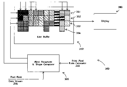
2o Buffering anc~ Display System c~~rating
Referring to Figure 3, pixel plates from image
capturing sub-system 200, are transmitted as a pixel plate
data stream 290 to a first embodiment of a Pixel Data
Buffering and Display System.,
In operation, a pixel placement & shape generator 360
receives and places the pixel plates 120, 125, etc., from
pixel plate data stream 290 into the correct positions
within a Line Buffer 350. This is accomplished using one
of the following methods:
(1) in an embodiment where the image capturing sub-
system 200 is remote from the sub-system 300, a
pixel plate pseudo-random generator "key" is
transmitted as part of the pixel plate data stream
290. This key is used by the pixel placement &
-12-
~~'~~~~~
shape generator 360 to reconstruct and properly
place the pixel plates 110 in Line Buffer 350. For
example, pixel plate 120, comprised of pixels A, B
and C on lines 101 and 102 in Figure 1, can be seen
to occupy a corresponding position on lines 351 and
352 of Line Buffer 350 in Figure 3.
(2) alternatively, in another embodiment, a pre-
conditioned pseudo-randoat sequences within pixel
placement & shape generator 360 can operate
independently to reconstruct the pixel plate
sequences.
These are but two possible techniques, and other equally
usable methods will become apparent to the those skilled
in the art. Additionally, if the pixel plate inforanation
in the pixel plate data stream has been data compressed,
pixel placement & shape generator 360 first dec~mpresses
the pixel plate data using a corresponding decompression
algorithm.
The output from the pixel placement and shape
generator 360 is sent to a mufti-line buffer 350. The
output of the mufti-line buffer 350 can be used to drive
any kind of display 380, including an active matrix
display, or a Digital-to-Analag Converter (DAB) connected
to a CRT, In this first embodiment, therefore, the images
are generated by the image capturing sub-system 200 at a
fixed rate D (72Hz in a preferred embodiment), and then
displayed at this same rate (72 Hz) on a display 380.
Alternatively, the output of the mufti-line buffer
350, since it is now back in a common video format, can be
further transmitted to a remote display receiver, via any
suitable land link, or broadcast transmission.
9eaond B~bodi~ex:t: Da~sic pia~1 Data
Buffesiag and Diaplag ~yat, In.c~luding fra~~ Buff~r
Another embodiment of the Pixel Data Buffering and
~~'~ ~'~'w~.
-13-
Display System is shown in Figure 4. This embodiment
includes a frame buffer 470 that accumulates higher
quality pictures and transmits them to one or more
displays 480 in the manner now described. The
accumulation of a better picture can be made when the
image is still, is motion compensated or when using film
or other slower media at their slower frame rate F (e. g.
24 Hz). An example of motion compensatian using motion
vectors can be seen in U.S. Patent ado. 4,985,767: other
similar techniques could be used with the present system.
The accumulation of multiple fast lower resolution images
forms higher quality frames at a slower rate.
As indicated above, the embodiment of Figure 3
captures images at fixed rate D using the image capturing
sub-system 200. In the embodiment of Figure 4, an image
capturing sub-system 200 can be used, but multiple frames
at the lower resolution rate D (e.g. 72 Hz) are
accumulated in Frame Buffer 470 to result in higher
resolution images at another rate F. In a preferred
embodiment, D is 72 Hz and F is 24 Hz: again, other values
of D may be used (e.g. 50 Hz, 60 Hz, 75 Hz, 80 Hz, 90 Hz
and 96 Hz may be useful for same applications), and other
values of F may be used (e.g. 36 Hz, 30 Hz, 25 Hz, 20 Hz
and 18 Hz.) Groups of D/F (e. g. 3) captured lower
resolution image frames are stored in Frame Buffer 470:
this corresponds to a higher resolution picture frame rate
F (e.g. 24 Hz, or 24 fps for film) that can be viewed on
display 480. The pixel group frames (D rate lower
resolution image frames containing pixel plates) should be
designed so that as many as possible of the individual
pixels are covered in the resulting F rate higher
resolution image. For longer accummulations of pixel
groups (e.g. F/2 or 12 Hz, or 2D/F frames at D rate) all
of the pixels should be covered.
~;~~~~:~1.
-14-
In operation, an input line consists of a pixel data
stream 290 from sub-system 200. This data stream 290 is
received and re-created in proper pixel plate placement in
mufti-line buffer 450 in an identical manner to that
described far Figure 3. Referring to Figure 4A, pixel
glate frame 401, generated at the D rate, is stored in
Frame Buffer 4?0. Then, frame 401 is read during the
receipt of the next frame 402, and the two are combined to
produce a higher quality resulting frame. This resulting
frame is then re-written into the frame buffer 470 (or a
separate frame buffer that is generally part of frame
buffer 470). The process is repeated D/F (e. g. 3) tames
to obtain the best quality higher resolution image.and is
then sent to the display each time with the display
updated at the D rate. This higher quality image can be
continually updated at the D rate, using the previous
((D/F)-1) frames, combined with the current frame. This
produces a steady-state running update at the D rate.
Referring to Figure 4B, it can be seen that in this
mode of operation, each pixel plate 120 from the pixel
plate frames 401, 402, 403, fills an average of D/F (e. g.
3) pixels in a D rate frame, but only contributes to a
single pixel at the final F rate frame 410 (e.g. after 3
frames at the D rate). Each pixel plate from the D rats
frame is centered over its corresponding position on the
F rate frame, and the three separate pixel plate sets from
the three frames are relatively orthogonal, as discussed
above. Thus, for example, in Figure 1, pixel plate 120
(pixels A, B and C) is centered about pixel A; pixel plate
125 (pixels D, E, F and G) is centered about pixel F, and
similarly for the rest of the pixel plates in any pixel
plate frame.
Finally, as also indicated abcwe, such groupings of
D/F (e.g. 3) frames can be stored in a separate section of
-15-
the frame buffer 470, and sent to the display with a D
(e.g. 72 Hz) refresh rate, where 'the frame is updated at
the F (e.g. 24 Hz) rate, or updated as a running update at
the D rate, covering roost individual pixels using the
previous ((D/F) - 1) frames, where the image is sent to
the display operating at the F rate.
~hir~l Rn~diment:~ via ~i~a~l Dstan
buffering and Display cyst, ~noltading ~'ra~g. Duff~r
and E~ana~ne~at 'knit
While the second embodiment of Figure 4 allows higher
resolution images as a result of accumulating lower
resolution images, this method is limited, as described
earlier, to situations where the image is still, is motion
compensated, or when using film or other slower media.
The capability of the Figure 4 embodiment may be
significantly improved, however, with the use of an
enhancement circuit 590 as shown in Figure 5.
Referring to Figure 5, the enhancement circuit 590
assures that when the imagery is fast-moving, and needs to
change at the faster D rate, then display 580 updates
directly at the D rate, without accumulating higher
resolution F rate frames through multiple frames at the D
rate. When the imagery is not fast-moving, frames are
accumulated using enhancement to obtain higher displayed
resolution. The determination of whether the imagery is
fast-moving or not involves examining regions of pixel
plates in the faster D rate frames. For example, in the
present system, enhancement circuit 590 examines regions
of 64 pixels (8 by 8 squares). The structures and methods
for performing such motion detection are well-known in the
art, and can easily be implemented by the skilled artisan
in the present invention. Motion compensation can also be
used when a displacement vector is used to select
appropriate locations in previous frames at the D or F
-16-
rates to provide input to the enhancement circuit.
Referring to Figure 5, the pixel plates from a frame
501 are processed and placed in multi-line buffer 550 by
pixel placement & shape generator 560, in the same manner
as described above for the Figure 3 and 4 embodiments.
Frame 501 is also stored in frame buffer 570. A portion
of frame 501 can be seen in the lower part of Figure 5,
including pixel plate 513, and an individual pixel denoted
"X." A new frame 502 is also shown: as can be seen, a
different pixel plate 512 overlaps with the pixel plate
511 in the area of pixel X. The values of the prior pixel
plates 511, 512 from pixel frames 501::. and 502 are
retrieved from a pixel plate buffer within the pixel
placement & shape generator 560,. or from the frame buffer
~5 570. Some deduction can be made from pixel plate 511 and
512 values as to the individual value of pixel X. In the
present embodiment, a weighting scheme is used that
depends on the geometry of the camera, the pixels, the
lens, and the pixel plates. .~ gaussian spot can be used
as a model for the pixels based on the values from the
pixel plates. In such a spot, a well-known pyramidal
weighting function is used to estimate the value of the
individual pixels in the pixel plate. Other methods known
in the art could also be used to evaluate the value of
individual pixels.
As the third frame 503 is processed, a determination
is made as to whether the general region where the pixels
are located is not moving or can be motion compensated: if
this region is fast moving (i.e. is not stationary or
cannot be motion compensated), the pixel plates (including
pixel plate 513) are placed directly in the mufti-line
buffer 550, frame buffer 570 and to the display 580. If
the region is not fast moving, the value of pixel X is
estimated from pixel plate 513, and then combined with the
t
i
_17_
information concerning pixel X that has been gleaned from
the prior frames 501 and 502 is used to arrive at a
differentially computed final value for pixel X.
Fourth ~bod3maeat: F~t~r ~ge cmpturing
Sy~te~ Using Pix~1 ~r~a~ ~aan~rl~tio~~s
of pig~1 plat~~
Figure 6 illustrates the basic buffering and display
system for the second mode of operation of the present
invention. As indicated above, this mode of operation
uses a camera frame rate higher than the display rate. In
a preferred embodiment, this camera frame rate is the LCM
(least common multiple) rate (e. g. 1800 Hz), of various
target display rates described above (24 Hz (fps), 25 Hz
(fps), 50 Hz, 60 Hz, 72 Hz, and 75 Hz) as used in the film
' industry, NTSC, PAL, HDTV, computer displays, etc.
Faster Imag~ Capturing Uubsyste~
Referring to Figure 7, it can be seen that the camera
or frame capturing device produces frames at the Lt~i .rate
888888with pixels scattered in special pseudo°random
distributions. When a real image 705 is imaged through a
video camera 710 including a lens 712 and an imaging
target plane 711 (a video camera), pixel plates are
scattered on imaging target 711 in a special Poisson°like
distribution, illustrated in magnified section 730.
In Figure 7, pixel groups are created directly by
video camera 710 as a pixel plate data stream 790 under
control of a pixel plate generator 740. Pixel plate
generator 740 includes pixel plate mappings previously
discussed with reference to pixel plate generator 240 in
Figure 2. Alternatively, therefore, the pixel groups
could be created using the sub-system shown in Figure 2.
A pixel group corresponds to one LGM frame time's Worth of
pixel spots containing pixel plates. A series of pixel
groups 810 can be seen in Figure 8.
~~»~~~~
-~s-
Displag o~ the Pix~l group
Referring again to Figure 6, a similar buffer and
display system to Figure 5 can be seen, except that a
pixel group accumulator 640 and pixel shaper 645 is also
used. Pixel group accumulator 640 is used since each
pixel group, comprised of a series of pseudo-randomly
distributed pixel plates captured at the higher LCP~i rate,
is only a portion of a lower rate viewable frame, and is
not directly viewable as are the pixel plate frames 401,
402, etc., discussed above in connection with Figure 4A in
operating mode one. Referring back to Figure 8,
therefore, it can be seen that frames 820A, 8208 and 820C
are viewable at a rate H1, while frames 830A, 830H and
8306 are viewable at rate H2. Frame 820A, for example, is
madewp of a number (I~/H1) of pixel group frames.
In general LC~i/H~ frames form a viewable frame,
wherein all of the pixel plates are nearly a closely
packed configuration. The pixel plates accumulation into
a viewable subframe may differ slightly from closer
packing with some small amount of overlap, uncovered
pixels, or both. These properties are controlled by the
pixel placement and shape generation algorithm or pre-
stored look-up tables.
Pixel shaper 645 processes the incoming pixel plates
from pixel plate data stream 790, and places them into the
proper spatial locations in accumulator 640. In this
manner, shaper 645 reconstructs the image created on the
imaging target 711 in the accumulator 640. The
accumulator 640 and shaper 645 architectures are
relatively simple and flexible, and any number of designs
can be easily implemented by a skilled artisan.
The fact that the pixel groups are not directly
viewable in this embodiment on a frame-to-frame basis does
not necessitate, however, the use of accumulator 640 and
-19-
shaper 645. Through suitable control electronics known in
the art, a collection of the smallest number of viewable
pixel groups could be accumulated as a viewable frame in
frame buffer 670. This viewable collection could then be
sent directly to display 680.
The advantage of the present invention is now readily
apparent. The data stream 790, because of its unique hCM
pixel group format, is usable by any number of target
display systems, and thus can be transmitted to all of
them. In each target display system, buffer and display
sub-systems accumulate the correct number of pixel groups.
For a system where the highest displayed frame rate
is H (e.g. 75 Hz) , the pixel distributions are designed so
that an accumulation of LCM/H (e. g. 1800/75 = 24) pixel
groups--in accumulator 640 results in a very nearly or
fully close-packed pixel accumulation allowing fully
detailed view of the scene in the real image 705. In
addition, when more pixel groups are accumulated
corresponding to a slower picture rate S (e. g. 24 frames
per second), then LC~i/S frames (e.g. 1800/24 = 75) of
these pixel groups combine to produce an even higher
quality image. This process can be seen in Figure 8,
where more pixel groups are used to create viewable frames
at the H2 rate than at the H1 rate. As with the method
used and described above to optimize the placement of the
pixel plates within each pixel group, the grouping of new
pixel groups with old pixel groups within the accumulator
640 can result in increasing sharpness using non-moving
images or motion compensated images as more pixel groups
are added to the viewed frame. These groupings may start
on any particular LCM pixel group. The pixel group
relative placements can be generated through proper
computer simulation using known techniques.
-20-
High~r Resolution 3.mag~s ilsing ~ahnnce~st~at
A higher quality image at the S rate (e.g. 24 fps) is
obtained by using the enhancement circuit 690 to perform
difference computations as described in connection with
Figure 5 for the first mode of operation. These
difference computations allow the overlap of the pixels to
be used in a computation which determines implied values
for pixels in a higher resolution frame. This allows a
higher resolution frame to be displayed where motion at
the H rate (e.g. 75 Hz) is not fast motion, or can be
motion compensated, but where motion at the S rate (e. g.
24 fps) captures the picture in full detail. This is
practical for those frames or portions of frames where the
image moves very little during the H/S frames (e.g.- approx
3) at the f~-. rate (e. g. 75 Hz) or can be motion
compensated.
In enhancement circuit 690, each pixel at the H rate
(e.a. 75 Hz) is compared with previous frames at the. H
(e. g. 75 Hz) rate to see if there is difference above some
threshold. The comparison can be made using known motion
compensation techniques. If the pixels within a region
change significantly above some threshold, then the
differential process for inferring higher resolution at
the S rate (e. g. 24 fps) is not invoked. This indicates,
for example, that the image is moving too rapidly. If for
some other region or frame, the pixels are similar within
some region, then a higher resolution picture frame can be
constructed which accumulates frames at the S (e.g. 24
fps) rata or even slower, if appropriate, although the
image may be updated at the H (e. g. 75 Hz) rate. This
method can be easily extended to any number of frames at
the H rate (e. g. 75 Hz) that can be inferred by using
multiples of pixel groups at the LCM rate (e. g. 1800 Hz).
An example of this method in operation can be seen in
-21-
Figures 9 and 10.
Due to varying image motion, the foregoing method
does not ensure that the same number of pixel
differentials are used for each frame grouping at the
resulting rate. However, the pseudo-random scattered
nature of the pixel plates within pixel groups allows
detail improvement to be relatively uniform over the
entire frame, even in this partial frame accumulation
case.
The use of enhancement based upon differential
computation is best used when such processing tame is
longer than the frame time (e.g. 13.33 milliseconds) of
the H rate (e.g. 75 Hz). Differential spot shape and
placement knowledge is provided by the pseudo-random
patterns which are genera~:ed as part of the F~oisson-like
pixel plate placement. This knowledge can be used for any
accumulation of pixel groups in excess of the minimum
LGM/H~ number._. _
Ths ~i~i I~t~
Any collection of pixel groups beyond the minimum
number of L~i/H~ (e.g. 1800/75 or 24 pixel groups) in the
accumulator 640 is viewable. Thus all display rates
slower than H~ that are divisible into LCM can be
accommodated by the present system. In Figure 7,
therefore, the pixel data stream 790 can be received by
any system operating at one of the hC,'M divisible rates.
The LCM, or camera frame rate, can vary, depending on
the nature and number of target display rats to be'
accommodated. For example, in the U.S., if 1/600 second
is used as the sampling interval (LChi), 24 Hz (used for
movie film) may be accommodated, as well as 25, 50, 60,
and 75 target rates. With 1/1800 second, 72 Hz may also
be directly extracted.
As an example, most adjustable multi-sync computer
~~ .i v...r~...~~.
-22-
display screens can operate at either 72 Hz or 75 Hz;
therefore, using a system with 1/600 second sampling is
possible. For those images originated at 24 Hz, the
display adjusts itself to 72 Hz. Using this idea, for all
other pixel group-constructed material, the display
operates at 75 Hz.
With appropriate dithering techniques, it is possible
to accommodate even non-standard rates that are not evenly
di~tisible into the LCM. For instance, if a display rate
was 39 Hz, and the LCM was 600, the target display and
buffer system accumulates 15 or 16 pixel groups at a time.
This method uses a nearest integer approach, and results
in an acceptable image with only minor errors.
For 600 Hz pixel groups, the number of pixel groups
in each viewable time interval which need to be
accumulated are as follows:
Rate # of 600 Hz pixel group
frames
U.S.Film 24 25
Europe Film 25 24
Non-Standard 39 15/16
Europe TV 50 12
U.S. TV 60 10
Computer 75 8
Thus, for any particular display rate, the present
invention provides an appropriate number of pixel group
f tames .
0th~r B~hodia~~nts ~» source auto-synohroni~~s
The present invention pan also be used as a source
auto-synchronizer. As shown in Figure 11 a computer
display 1000 receives multiple signals from multiple
sources S1, S2 and S3. To display all possible source
signals, a number of data buffers 1011, 1012 and 1013 are
typically required to synchronize the input sources on the
F
-23-
same display screen.
In a typical environment, the data input sources
S1,
S2, S3 could include satellite transmissions, professional
broadcasts, computer networks, fiber-optic networks,
teleconferencing channels, etc. The speed of light
is
300, 000 kilometers per second, and display frame
rates are
between 10 to 7.00 milliseconds. the difference between
a
source located 1 kilometer away, and another at 2,001.
kilometers away is 2,000 kilometers, or about 6
milliseconds. Many potential situations of multi-signal
data signals thereby involve processing signals from
sources at various distances that span a significant
portion of a frame time, and thus are delayed in
varying
amounts under ordinary circumstances. In a typical
~
environment, therefore, the data buffers 101.-:.,
~ 1012 and
1013 provide the necessary synchronizing by providing
an
additional layer of buffering of the data that contains
different synchronizing times. ..
It is a property of operating mode 2 of the pixel
interlaced signal that frames have arbitrary starting
times and can naturally adapt to any display rate,
thus
obviating the need for additional data buffers. Referring
back to Figure 6, the input data stream described
in
connection thereto can include several data sauxces.
For
example, originating signal source S1 could be running
at
75 Hz using 600 Hz pixel groups, another source S2
could
run at 60 Hz using 600 Hz pixel groups; and a third
source
S3 could run at 50 Hz using 600 Hz pixel groups.
These
values are given only for explanation, and any LCM
rate
could be used by the signal sources.
If a display in Figure 6 is panning at 24 Hz, a pixel
group accumulator 640 processes 25 pixel group frames
combined from the three sources in a fast frame buffer
before updating the display. These image accumulations
-24-
can start at any individual pixel group frame start time
(every 1/1800 sec.) Thus, a wide variety of signal
sources can be displayed simultaneously without the need
for buffering capability.
In summary, the present invention, by using a pseudo-
random pixel interlacing method, eliminates the artifacts
commonly present in standard line raster scan imaging
systems. I~toreover, this novel pixel interlacing method
permits the construction of higher resolution frames from
a series of orthogonal lower resolution frames. The
enhancement circuit of the present unit deduces .
information from previous pixel group frames and
contributes additional detail to the pixels of the frame
being processed. The format of the pixel interlaced data
" stream permits the-present invention to be used in a~-wide
variety of normally incompatible target display rates.
Finally, the present invention can be used as an auto-
synchronizer.
The foregoing illustrates but a few embodiments of
the present invention. ~ther variations will be apparent
to the skilled artisan. Accordingly, the scope of the
present invention is to be determined by the following
claims.