Note: Descriptions are shown in the official language in which they were submitted.
2 ~ 3
SYSTEM CLOCK SWITCHING MECHANISM FOR MICROPROCESSOR
BACKGROUNDS OF THE INVENTION
FIELD OF THE INVENTION
The present invention relates to a system clock
switching mechan$sm used in a microprocessor which
operates with a plurality of system clocks (CPU system
clocks) at different speeds.
DESCRIPTION OF THE PRIOR ART
Some conventional microprocessors are provided with
two system clocks switched by a real time operating
system- a system clock of low clock frequency, i.e. a
clock at a low speed (hereinafter referred to as a low
speed clock) and a system clock of high clock frequency,
i.e. a clock at a high speed (herei.naf~er referred to as
high speed clock).
A conventional system clock switching mechanism
using a real time operating system for such
microprocessors is briefly described below. In the
conventional ~ystem clock switching mechanism, the
system clock is switched from high speed to low speed if
no task (user task) is in READY or RUN status. If any
task is in READY or RUN status, the systam clock is
switched from low speed to high speed when the
applicable task is put in RUN status.
If no task is in READY or RUN s~atus and the
microprocessor is in HALT status, the system alock is
2 ~ 3
switched to low speed. This reduces the power
consumption and noise (so called CPU noise) caused by
the microprocessor. If a task is put in READY status
(by hardware interrup-tion, for example), with the
microprocessor in HALT status, the system clock is
switched to the high speed clock at the moment that task
enters RUN status, which enables high speed processing
of the task.
The system clock switching mechanism of
conventional microprocessors as described above realizes
low power consumption at the microprocessor and reduced
CPU noise by switching the system clock to the low speed
clock when no task is in READY or RUN status and
switching it -to the high speed ciock at the moment a
task enters RUN status. However, the effect of power
consumption reduction and CPU noise lowering as
described above i8 limited because the æys~em clock
switches to the high spe2d clock every time when a task
is put in RUN status. No~ all of the tasks executed on
the microprocessor need to be processed with the high
speed clock. Some of the tasks can be processed with
the low speed clock without causing any problern~ If the
tasks which can be processed at a low speed are
processed with the low speed alock, it will achieve
further reduction of power consumption and CPU noise at
the microprocessor.
~6~3
SUMMARY OF THE INVENTION
The object of this invention is to provide a system
clock switching mechanism whare the systam clock can be
specified for each task so that the power consumption
and CPU noise while a task is run by the microprocessor
can be reduced.
According to a preferred embodiment of the present
invention to attain this object, a system clock
switching mechanism is provided with a clock generating
means to supply a plurality of system clocks at
different speeds to the microprocessor, a holding means :
to set and hold the system clock specification data for
each task e~ecuted by the microprocessor, and a clock
switchi~g means to switch the system clock supplied by
the clock generating means. The clock switching means
switches the system clock to -the clock specified for
each task according to the system clock specification
data held by the holding means.
According to a preferred embodiment, the clock
switching means switches to the lowest speed system
clock when no task is in READY or RUN stat~s, and
switches to the system clock as specified when such a
task e~ists accord1ng to the system clock specification
data held by the holding means. According to a further
preferred embodiment, the sys~em clocks provided by the : -
clock generating means are two: low speed clock and high
, ., . ~
'' :.
. ` :,
8 ~ ~
speed clock.
The sys~em clock switchlng m~chanism for a
microprocessor according to another preferred embodiment
of this invention is provided with a clock generating
means to supply a plurality of system clocks at
different speeds to the microprocessor, a holding means
to set and hold the system clock specification data for
each ~ask executed by ths mlcroprocessor, a scheduler
means to judge whether there is any task in READY or RUN
status ~nd refer to the system clock specification data
held by tha holding means for each task, and a clock
switching means to switch the system clock supplied by
the clock generating meansO When the scheduler m~ans
judges that thare is no task in READY or RUN status, the
clock switching means switches to the lowest speed
system clock, and when ~he scheduler means judges that
there is any task in READY or RVN status, it refers to
the system clock specification data held by the holding
means and instruct the clock switching means to switch
to the system clock given by the system clock
specification data. The clock switching means switches
between the system clocks according to the switching
inætruction from the scheduler means.
Other objects and effects of the present invention
will be clarified by the detailed description below.
-
.:
~ ' ' ' '
.
: ~
2 ~ 3
BRIEF DESCRIPTION OF THE DRAWINGS
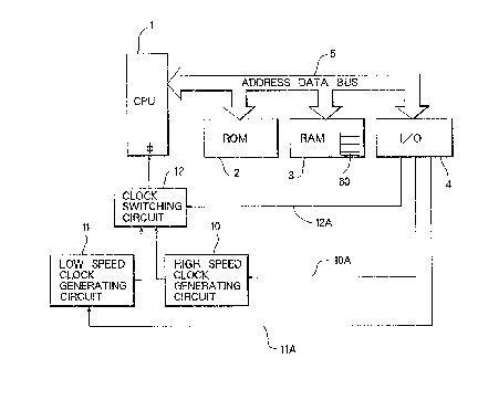
FigO 1 is a block diagram to show the entire
configuration of a microprocessor system according to a
first embodiment of the present invention.
Fig. 2a, Fig. 2b is a block diagram to show the
function of the real time operating system to realize
the system clock switching mechanism of ~his invention,
also serving as a flowchart to show its operation.
~ESCRIPTION OF THE PREFERRED EMBODIMENT
Referring to Figs. 1 and 2a, 2b a preferred
embodiment of the present invention is described now.
Fig. 1 shows the configuration of a microprocessor
systam with the system clock switching mechanism
according to the first embodim~nt of the present
invention.
In Fig. l, a microprocessor system according to
this embodiment comprises a microprocessor (CPU) 1 and a
ROM 2, a RAM 3, and an I/O interface 4 connected to the
microprocessor 1 via an address/data bus 5 and a high
speed clock generating circuit 10, a low speed clock
generating circuit 11, and a clock switching circuit 12.
The ROM 2 accommodates a real time operating system
and a service macro uni~, an interrup~ion service macro
unit, and a register return/stack pointer setting unit
as programs in advance. The RAM 3 is a memory area to
2 ~ 3
store user programs and data. In this embodiment, a-task control table (TDB) 60 as described later is set in
the RAM 3.
The high speed clock generatiny circuit 10 and the
low speed clock generating circuit 11 serve for
g~nerating system clocks at high speed and low speed
respec~ively for operation of the microprocessor 1.
They are connected to the I/0 interface 4 via a high
speed clock control line lOA and a l ow speed clock
control llne llA. The high ~peed clock generating
circuit 10 and the low speed clock generating circuit 11
can senerate and stop clocks according to the control
signal from the microprocessor 1 sent via the high speed
. clock control line lOA and the low speed clock control
line llA. However, clock.s are not necessarily
controlled for generation and stop. They can be left to
continue generation all the time.
The clock switching circuit 12 is capable of
supplying the system clock to the system clock 1 in the
microprocessor 1 by switching between the high speed
clock generating circuit 10 and the low speed clock
generating circuit 11. It is connected to the I/O
interface 4 via a clock input switching line 12A.
Switching operation is controlled by the control signal
sent from the. clock switching control unit (described
later) via this clock input switching line 12A.
.
- , . . : ~: . :
, ., - . :
' ~
2~8~3
Switching between the high speed clock generating
circuit 10 and ~he low spe~d clock generating circuit 11
is made at a rise of the clock or oth~r timing.
Next, referring to the functional block diagram and
flowchar~ of Fig. 2a, 2b this system clock switching
mechanism i9 described. Fig. 2a, 2b is a block diagram
to show the functlon of the real time operating system
to achieve this system clock switching mechanism and at
the same time serves as a flowchart to show its
functlon. ~n Fig. 2a, 2b the numeral 20 indicates a
service macro unit, 25 an interruption service macro
unit, 50 a register/stack pointer (SP) processing unit
for register return and stack pointer setting. The
service macro unit 20 controls macro operations such as
WAIT ma~ro processing 21, POST macro processing 22, EXIT
macro proc~ssing 23 and CUT macro ~rocessing 24. The
interruption service macro unit 25 controls interruption
processing 26, which may be caused by hardware
interruption, for example.
The numeral 30 indicates a scheduler unit and the
numeral 40 indicates a clock switching control unlt.
The scheduler unit 30 controls tasks executed by the
microprocessor 1. The clock switching control unit 40
controls the clock switching circuit 12 as described
above corresponding to the task status so as to switch
the system clock properly.
,
8 5 ~
--8--
The service macro unit 20, the interruption service
macro unit 21, the scheduler unit 30, the clock
switching control unit 40, and the register/SP
processing unit 50 are all embodied in the real time
operating system and stored in the ROM 2 of Fig. 1 in
advance.
The TDB ÇO ls a table to specify the speed of the
system clock for e~ecution of a task (user task) by thQ
microprocessor l as a data (system clock specification
data~ and is set in a part of the RAM 3 as described
above.
This TDB 60 comprises a plurality of tables 61, 62
... corr~spon~ing to a plurality of tasks. For e~ample,
~he table 61 stores the system clock specification data
for task A and the table 62 stores the sys~em clock
specification data for task B. All system clock
specification data for the tasks are similarly stored.
Here~ the table 61 for task A stores X, which
indicates the high speed clock, as the system clock
specification data. ~he table 62 for task B stores Y,
which indicates the low speed clock, as the system ~lock
specification data.
The system clock switching operation will be
described below.
The scheduler unit 30 judges whether there is a
task in READY or RUN status (301)~ If such a task is
, . ~
2 ~ 3
g
not found, the scheduler unit 30 requests the clock
switching control unit 40 to switch to the low speed
clock. In response to this, the clock switching control
unit 40 judges whPther the microprocPssor 1 is currently
operating with the high speed clock or not (401~. If it
is operating with the high speed clock, the clock
switchin~ control unit 40 sends the switching signal to
the clock switching circuit 12 to switch the high speed
clock to the low speed clockO This causes the system
clock to the microprocessor 1 to be switched to the low
speed clock at the clock switching circuit 12. Then,
the m~croprocessor 1 is put in HALT status.
If the scheduler unit 30 judges that there is such
a task in Step 301, it makes the tasks to be put in RUN
status ~if any) enter RUN status (302). Then, it refers
to the TDB 60 to look for the system clock specification
data corresponding to the tasks in RUN status (303).
For task A, the system clock specification data X in the
table 61 of the TDB 60 iS obtained, and for task ~, the
system clock specification data Y in the table 62 of the
TDB 60 is obtained. As a result of reference to ~he TDB
60, if the low speed clock is specifie~ for that task
(task B, for example), the scheduler unit 30 requests
the clock switching control unit 40 to switch to the low
speed clock, and i~ the high speed clock is specified
for that task (task A, for example), it requests the
8 ~ 3
--10--
clock switching control unit 40 to switch to the high
speed clock.
The clock switching control unit 40, upon request
by the scheduler unit 30 to ~witch to the low speed
clock, judges whether the microprocessor 1 is currently
operating with the high speed clock or not (403). If it
operates with the high speed clock, the clock switching
control unit 40 instructs the clock switching circuit 12
to switch the æystem clock from the high speed cloc~ to
the low speed clock (404). This makes the system clock
in the microprocessor 1 switched to the low speed clock.
When Step 404 terminates or when it is judged that the
microprocessor is not operating with the high ~peed
clock currently, the register/SP processing unit 50
returns the register and performs other processing (501)
for returning.
When the scheduler unit 30 requests switchiny to
the hi~h speed clock, the clock switching control unit
40 Judges whether the microprocessor 1 is currently
operating with the low speed clock or not (405). I f it
is operating with the low sp ed clock, the clock
swit~.hing control unit 40 instructs the clock switching
circuit 12 to switch the system clock from the low speed
clock to the hlgh speed clock (A06). This makes the
system clock ln the mlcroprocessor 1 switched to the
high speed clock. When Step 406 terminates or when the
~ .
2 ~ 3
microprocessor is not operatiny with the low speed
clock, the register/SP processin~ unit 50 returns and
performs other processing for return.ing.
As obviously learned from the description above,
when no task is in READY or RUN status and the
microprocessor 1 is in HALT status, Steps 401 and 402 at
the clock switching control unit 40 switch the system
clock to the low speed clock. This reduces the power
consumption by the microprocessor 1 and lowers the CPU
nois~ it generates.
Assume now that the interruption service macro uni~
25 in the real time operating sys-tem is executed by
hardware interruption, for example, when -the
microprocessor is in HALT status and a POST macro which
cancels WAIT status of task A is :issued. In this case,
task A enters READY status and then is put to RUN status
at Step 302 by the scheduler unit 30. At Step 303, the
scheduler unit 30 refers to the system clock
; specific~tion data X in the table 61 of the TDB 60 and
requests the clock switching control unit 40 to switch
to the high speed clock, and the clock switching control
unit 40 proceeds to Step 406 to switch the system clock
to the high speed ~lock, and then to pass the control to
task A.
If, on the contrary, task B is in READY status when
the microprocessor is in HALT status and the control is
2 ~ 3
-12-
to be passed to task B, the system clock specification
data Y in the table 62 of the TD~ 60 is referred to and
the scheduler unit 30 requests the clock switching
control unlt 40 to switch to the low speed clock. The
clock switching control unit 40, since the
microprocessor is currently operating with the low speed
clock, jumps from Step ~04 to Step 501. Then, task B is
executed with the low speed clock. 0 course, if the
microprocessor is operating with the high speed clock
before the control is passed to task B, the clock
switching control unit 40 performs Step 404 to switch to
the low speed clock.
As described above, the system clock switching ~:
mechanism of the present invention enables specification
of system clock for each task by the system clock
specifiaation data held by the memory means such as TDB
60. Therefore, by setting the system clock
specification data to instruct the use of low sp~ed
clock for the tasks which can be properly processed at a
low speed, those tasks are processed with low speed
clock. This promotes reduction of power consumption and . ` .
CPU noise at the microprocessor
While the invention has been described in its
preerred embodiments, it is to be understood that
various modifications may be made therein. For example,
there are two system clocks for high speed and low speed
, .. ... . ..
.; ~ .
:. :
~13-
in the a~ove embodiment, but switching can be made for
increased number of degrees. For example, it is
possible to provide three degrees including high speed,
medium speed and low speed clocks. Naturally, for
increased system clocks, the TDB 60 will have ;
correspondingly increased system clock specification
data. It is intended to cover in the appended claims
all such modifica~ions as fall wlthin the true spirit
and scope oi the invention.