Note: Descriptions are shown in the official language in which they were submitted.
-
FR9-90-016 1 2 0 6 0 9 7 6
DATA CIRCUIT TERMINATING EQUIPMENT (DCE) AND METHOD FOR
PROCESSING DATA RECEIVED IN A DCE ALLOWING MULTIPLE
OPERATING CONFIGURATIONS
The invention relates to data communication systems and more
particularly to the data circuit terminating equipments (DCE) allowing
multiple operating configurations.
DCEs which allow multiple operating configurations (for instance V25
bis, V42 ... according to the CCITT requirements) exist in the art.
Those DCE include a first digital signal processor DSP assisted by a
control processor processor used for handling the protocols, and more
generally a complex hardware circuitry (including switches, registers,
serial communication controllers) for m~n~g~ng the communication
between two of the Data Terminating Equipment (DTE) connected to the
DCE, the control processor, the DSP processor and the
telecommunication line in accordance with the considered protocole.
The latter circuitry involves a great deal of electronic components which
inevitably increases the complexity and the cost of the modem.
Moreover, the great number of electronic components required in DCE
known in the art, jeopardize the possibility of integration of the DCE
and particularly when the DCE is intended to be embodied into an
interface card for a workstation such as a personal computer.
Therefore a need has appeared for a simple DCE which does not require
a great deal of electronic components whilst allowing multiple
configurations .
Summary of the invention
It is an object of the invention to provide an apparatus for processing
data in a DCE which support `multiple configurations without
necessitating a great deal of electronic components.
~,
' ~.~
FR9-90-016 2 Q ~ n~ 7 6
It is another object of the invention to provide a DCE in
which an internal control processor can easily intercept the
sequence of data without requiring a complex electronic
switch.
It is a further object of the invention to provide a low
cost DCE supporting the CCITT V 25 bis, CCITT V42 bis, CCITT
V22 bis, CCITT V32, and forthcoming V17, V32 bis, "V fast"
recommendations and also providing control network
management functions.
It is another object of the invention to provide a method
for processing data conveyed through a DCE allowing multiple
configurations.
These and other objects of the invention are provided by
means of a new organization of the communication between the
different elements included into the DCE and particularly a
DSP processor used for the processing of data a control
processor for handling the communication protocols, the DTE
and the telecommunication line. More accurately, the
apparatus according to the present invention includes a
Memory in which are store different queues respectively
loaded with bits and characters coming either from the DTE
and the telecommunication line.
By providing logical connections between the different
queues, multiple telecommunication protocols are provided in
a simple device.
The invention provides a DCE which is capable of operating a
multiple configurations and without necessitating a great
amount of electronic components. The DCE is therefore much
more easy to integrate in an interface and for a workstation
and even in a single chip.
The invention also provides a method for processing data in
a DCE and received either from a DTE or the
telecommunication line thereto connected. The method
involves the steps of creating different queues in a memory
2050~76
FR9-90-016 3
which respectively stores the bits and the characters received either
from the DTE and the telecommunication line.
The logical connection between some of the better queues by means of
the appropriate management of the associated pointers permits the DCE
to operate in accordance with multiple telecommunication configurations.
The method particularly performs the processing of data into a DCE and
the DCE according to the present invention which includes a digital
signal processor DSP for processing the data transmitted between a
Data terminating equipment DTE and a telecommunication line, transmit
and receive circuits being connected to the DTE interface. The DCE
further includes A/D and a D/A converters for respectively converting
the data from an analog form to Pulse Coded Modulation PCM words and
from PCM words to an analog form and also a control processor for
controlling the communication protocols and a storage which is connected
to both the DSP processor and the control processor. The method is
characterized in that it involves the steps of storing by means of said
DSP processor the bits provided by said transmit circuit into a first
queue which is located into said storage and storing into a second
queue which is also located into the same storage the characters being
computed by said DSP processor and deriving from the bits stored into
said first queue accordingly to a first given tr~ncmi.~.cif-n protocol being
either a start-stop, a high level data link control (HDLC) or a binary
synchronous communication (BSC) transmission protocol. The method
further involves the step of storing into a third queue which is located
into the same storage as above the characters being provided by said
control processor in order to be transmitted to a remote DCE via the
telecommunication line. A further step is involved which is the storing
into a fourth queue which is also located in the storage, of the bits
being computed by said DSP processor and deriving from the characters
stored into said third queue accordingly to a second given tr~ncmi.CRi-~n
protocol. The transmission of data through the telecommunication line is
achieved by storing into a fifth qùeue the PCM words which are
computed by said DSP processor in accordance with a given modulation
algorithm, the PCM
FR9-90-016 4 2~0976
words being derived either from the contents of said first
queue in synchronous mode or from the contents of the third
queue when the transmit part of the DCE is intended to
operate in an asynchronous mode or still when the control
processor wishes to transmit data through the
telecommunication line. The selection of an appropriate
transmission protocol, which is chosen from existing
protocols such as start-stop, HDLC, BSC, as well as the
selection of the appropriate modulation algorithm which
provides a method for processing data to be transmitted from
a DTE to a telecommunication line, allow a large number of
configuration without requiring the great number of
electronic components which were usually necessary.
The invention also provides a method for performing the
receive part of a DCE. In that case, the method involves the
step of storing in a first queue, which is located in the
storage the characters being provided by the control
processor in order to be transmitted to the DTE. The method
involves the step of storing in a second queue which is also
located in the storage the bits being computed by the DSP
processor and deriving from the characters stored into the
first queue according to a third given transmission
protocol. In a third queue also located into the storage,
are stored the PCM words which are received from the A/D
converter. The method further involves the step of storing
by means of the DSP processor in a fourth queue also located
in the storage, the bits which are computed by the DSP
processor in accordance with a given demodulation algorithm,
the computed bits being derived from the PCM words loaded
into the third queue. In a fifth queue being also located in
the storage, are stored the characters which are computed by
the DSP processor and which are derived from the bits stored
in the fourth queue according to a fourth given transmission
protocol. The method according to the present invention
further involves the step of transmitting to the receive
circuit the bits coming from the fourth queue when the DCE
operates in a synchronous mode, or from said second queue
when the DCE operates in an asynchronous mode or still when
the control processor wishes to transmit data to the DTE.
Similarly as above, the choice of an appropriate
~^ ~
FR9-90-016 5
20~7~
transmission protocol such as the start-stop, HDLC or BSC
protocol for the third or fourth transmission protocol
provides, without necessitating a great deal of hardware
component, the possibility of numerous operating
configurations.
Description of the drawings
Figure 1 illustrates a multiple-configuration DCE which is
known in the art.
Figure 2 illustrates a multiple-configuration DCE in
accordance with the present invention
Figure 3 illustrates the arrangement of shared memory 204 in
accordance with the present'invention. `-
Figure 4 details the interrupt routines operated in the DCE
of the invention.
Figures 5A, 5B and 5C are views of a flow chart illustrating
the background program executed by the DSP. -
. . .
Description of the preferred embodiment of the invention :~
An example of a known DCE is illustrated with respect to
figure 1 which includes a first processor 100 for
controlling the protocols and a second processor 102 which
is used for carrying out real time signal processing
operations as well as bit flow control operations. For -~
achieving this, processor 102 is generally a digital signal
processor DSP having powerful signal processing
capabilities. Processor 100 particularly provides functions
in accordance with the CCITT requirements, for instance
functions in accordance with the V25 bis, the V 42 bis and
also the LPDA2 functions (Control Network Management
functions). For achieving this, processor 100 is~ associated
with a PROM storage 105 which stores a set of program
instructions and a RAM storage 101, both PROM storage 105
and RAM storage 101 being connected to a ~p bus 119
I
connected to processor 100. DSP processor 102 manages the
FR9-90-016 6 2 ~6 0 ~ 7 ~
signal processing functions such as those involved in the
CCITT V22 bis modem ~for full-duplex 2-wire transmission at
a rate of 2400 bps) or in the CCITT V32 modem (in the case
of full duplex two-wire transmission at a rate of 9600 bps).
DSP processor 102 is connected via a DSP bus 117 to a ROM
storage 103 and to a RAM storage 106. A serial communication
controller SCC1 110 is connected to bus 119 and receives
serial data on lead 127 from a switch 108 and generates data
in series to the latter switch 108 on a lead 128. The
appropriate clocks required for that purpose are provided on
a clock bus 118 which distributes clock signals generated by
a clock generator 132. The purpose of clock generator 132 is
to provide on clock bus 118 all the required clock signals
needed in the DCE and particularly the internal clock
derived from an internal oscillator (not shown), the receive
clock derived from the receive signal and also the external
clock provided by DTE 109. SCC1 110 supports the traditional
protocols known in the art such as SDLC (Serial Data Link
Control) or BSC. Similarly, a serial communication
controller SCC2 1ll is connected to bus 119 and receives
serial data on a lead 125 from switch 108 and also transmits
to switch 108 the serial data on a lead 126. A parallel
Input/Output (PIO) circuit 112 is connected to bus 119 and
permits to control switch 108 via leads 129. The control of
switch 108 by processor 100 via PIO 112 allows the DCE to
work in some different configurations. The generation of the
control signals at the DTE interface (for instance Data Set
Ready (DSR), carrier detect (CD) signals) are performed by
processors 100 and 102. Switch 108 achieves the connection
of the serial transmit data lead 131 and serial receive data
lead 130 existing on the DTE interface (with respect to the
CCITT V24 recommendation) to the different parts of the DCE
in accordance with the configuration as will be detailed
hereinafter. Switch 108 operates as follows: in the data
transfer mode, transmit data lead 131 is connected to lead
121 and conversely lead 122 is connected to receive data
lead 130. In this way, the data bits are directly
transmitted and received from the telecommunication line to
the DTE interface such as in a common datapump. In a second
communication mode corresponding to a calling phase
according to the V25 bis CCITT recommendation for a switched
FR9-90-016 7
20S~976
network, transmitted data lead 131 is connected to lead 127
and lead 128 is connected to received data lead 130.
Processor 100 communicates with DTE 109 via SCC 110 in
accordance with the V25 bis protocol, and has the
possibility to know the identity of the calling party etc...
As long as the calling phase does not complete, leads 121
and 122 remain unused since DSP processor 102 does not emit
any data.
The complexity of the DCE, and particularly in terms of
hardware components~ increases more when the DCE is intended
to work in a third mode which consists in the support the
Link Problem Determination Aid-2 ~LPDA-2) protocol since the
second SCC 111 and PI0 112 are particularly involved. The
LPDA-2 facility (for detailed information, see the IBM
document 'Link Problem Determination Aid', reference
SY33-2064-0) defines the general rules of communication
between the network and a DCE and particularly involves the
transmission of Control Network Management (CMM) commands
through the telecommunication network, the CNM commands and
the user data being transmitted through the same
communication channel. In that LPDA2 mode, processor 100
controls switch 108 via PI0 112 so that transmitted data
lead 131 is connected to leads 127 and 121 and, received
data lead 130 is connected to leads 122 and 125. Processor
100 continuously monitors, by means of SCCl 110, the data
appearing on transmitted data lead 131 (and transmitted to
lead 127) in order to detect the LPDA2 header. Similarly,
processor 100 continuously monitors, by means of SCC2 111,
the data which are conveyed on leads 122/125 in order to
detect the service message. At the detection of the LPDA2
header appearing on lead 127, processor 100 initiates the
execution of a LPDA2 command by disconnecting leads 122 from
received data lead 130 leads 122 remained connected to leads
125, and also by connecting lead 128 with received data lead
130. Simultaneously~ processor 100 disconnects lead 121 and
transmitted data lead 131 and connects lead 126 to lead 121.
From that instant SCC 110 is connected to the DTE and
conversely SCC1 111 is connected to the telecommunication
line. Processor 100 then initiates by means of the latter
SCC2 111 a service procedure with a given distant
~R9-90-016 8 2 ~ ~ ~ 9 7 ~
telecommunication equipment which is connected to the
telecommunication network. That distant telecommunication
equipment recognizes the service message by detecting on the
data channel the LPDA2 header and consequently process the
service message. When processor 100 has received and stored
the CNM data transmitted from the distant telecommunication
equipment while the CNM service message procedure, processor
100 transmits the LPDA2 answer via received data lead 130 by
means on SCC1 110 et returns to the mode-1 configuration
which was described above. In a fourth telecommunication
mode involving the V42/V42 bis CCITT recommendation, a phase
of data transfer with error correction protocol is involved
in response to a V25 bis calling phase. Processor 100
controls switch 108 by means of PI0 112 so that to switch
from a V25 bis procedure to a V42 procedure. In order to
perform the latter V42 procedure, the received data lead 130
is connected to lead 128, transmitted data lead 131 is
connected to 127, lead 126 is connected to lead 121 and lead
122 is connected to 125. SCC 110 is used in asynchronous
mode while SCC 111 is used in accordance with the SDLC
protocol under control of processor 100.
In all the configurations listed above, the DSP processor
102 operates as follows: the serial data bits coming from
lead 121 are deserialized by transmit block 113 which
transmits them to DSP processor 102 in n-bit-packets and in
interrupt mode. Transmit block 113 is controlled by the
transmit clock (ie internal or external according to the
desired configuration) which is conveyed on clock bus 118.
In accordance with the asynchronous V14 mode, transmit block
113 decodes the asynchronous characters that is to say
recognizes the start-bit and generates the deserialization
clock. Receive block 114 generates interrupt signals to DSP
102 so that the latter generates a n-bit-word on DSP bus
117. Then Receive block 114 serializes on lead 122 the
n-bit-word at the rate of the receive clock existing on the
clock bus 1;8. A digital-to-analog converter 116 receives
the samples which have been computed by DSP processor 102 in
accordance with the modulation algorithm, the latter
modulation being pulsed by the Xmit sampling clock which is
provided by clock generator 132 via clock bus 118.
FR9-90-016 9 20~0976 ~``
Similarly, an analog-to-digital converter 115 provides DSP
processor 102 with samples at the timing of the receive
sampling clock which is generated by clock generator 132 on
clock bus 118. The analog signals which exists on leads 123
and 124 are transmitted to, or from, the line interface
circuit 107 which eventually provides the appropriate
coupling to the telecommunication line. RAM 106 includes one
buffer into storage 104 for every direction. Therefore, the
Xmit bits provided by lead 121 are stored into a first queue
into RAM 106 and are then processed by DSP 102 in order to
generate the samples which are required to digital-to-analog
converter 116 and, converæely the samples provided by the
analog-to-digital converter 115 are processed by DSP
processor 102, the latter processing providing bits which
are stored into the second queue into RAM 106 before being
transmitted to lead 122 via receive block 114. The interrupt
signals appearing on DSP bus 117 and which controls Xmit
block 113 are synchronous with those controlling
digital-to-analog circuit 116 and similarly the interrupt
signals controlling receive block 114 are synchronous with
those controlling analog-to-digital circuit 115. The shared
buffer 104 connected to both bus 119 and bus 117 allows the
exchange of commands and between processor 100 and DSP
processor 102 and particularly allows the exchange of the
answers relating the status of the DCE: call phase, data
phase according to the CCITT V25 recommendation.
It therefore appears that the DCEs known in the art which
are intended to permit multiple telecommunication
configurations involve a complex and costly switch 108, a
PIO 112 including many registers, the existence of two SCC
circuit 110 and 111 and, more generally, a great deal of
hardware circuits and electronic components.
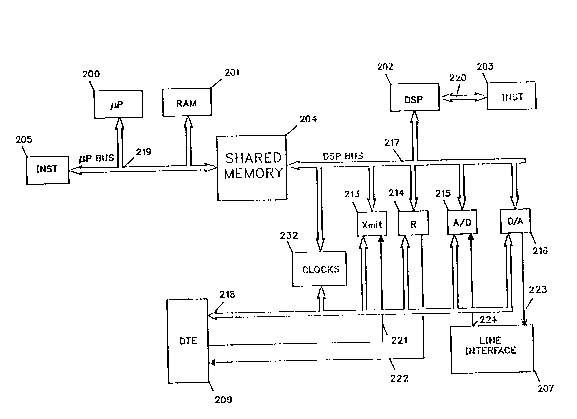
Figure 2 shows the preferred embodiment of the
multi-configuration DCE in accordance with the present
invention The DCE according to the invention includes a
processor 20~ for controlling the protocols which is
connected to a PROM storage 205 and a RAM storage 201 via a
bus 219. A Digital Signal Processor 202 connected to a PROM
storage 203 via a bus 220 is used for carrying out real time
FR9-90-016 10 2 Q ~ 0 9 7 ~
signal processing operations as well as bit flow control
operations. DSP processor 202 is connected via a DSP bus 217
to a shared RAM storage 204, the organization of which being
described in detail by figure 3. RAM storage Memory 204 is
also connected to the data bus of bus 219 in order to
provide a logical connection between both processor 200 and
202. A clock generator 232 provides a clock bus 218 with all
the needed clocks in the DCE and particularly an internal
clock which is derived from an internal (not shown)
oscillator, the receive clock which is derived from the
receive signal and also the external clock which is provided
at the DTE interface.
A Xmit block 213 deserializes the transmit data bits coming
from lead 221 at the DTE V24 interface. When a n-bit packet
is assembled, an interrupt for DSP processor 202 is
generated to indicate to this processor that th en-bit
packet can be read. Xmit block 213 is under control of
transmit clock provided on clock bus 218 teither the
internal or external clock or receive clock in accordance to
the desired configuration). According to the CCITT V14
Recommendation, Xmit block 213 also includes means for
decoding the asynchronous characters that is to say for
recognizing the start-bit and for producing the
deserialization clock.
A receive block 214 generates interrupt signals to DSP
processor 202 when it has to receive n-bit-words from DSP
processor 202 on bus 217. Then Receive block 214 serializes
on lead 222 the n-bit-word at the rate of the receive clock
which exists on the clock bus 218.
A digital-to-analog converter 216 receives the samples which =-`~
have been comp~ted by DSP processor 202 in accordance with ~-
the modulation algorithm, the latter modulation being pulsed `~
at the rate of the Xmit sampling clock which is also
provided by clock generator 232 on clock bus 218.
Similarly, an analog-to-digital converter 215 provides DSP ~-
processor 202 with samples at the timing of the receive ~
-? .~ .
2060976
FR9-90-016 11
sampling clock which is generated by clock generator 232 on clock bus
218. At last, a line interface circuit (207) which is connected to analog-
to-digital circuit 215 via a lead 224 and to digital-to-analog circuit 216
via lead 223 performs the appropriate coupling to the telecommunication
line .
Effective timing arrangement circuits for controlling , Xmit block 213,
receive block 214, analog-to-digital circuit 215 and digital-to-analog
- - circuit 216 are disclosed in U.S. Patent No. 5,315,622, issued May 24,
` 1994, entitled "Data circuit terminating equipment (DCE) including
timing arrangement circuits controlled by processing means" and
assigned to the assignee of the present application. Briefly, in
accordance with U.S. Patent 5,315,622, the control of those circuits is
achieved by storing a number of digital values in appropriate registers
Receive sampling (RS) time register (43), Transmit sampling (XS) time
register (53), a transmit data (TD) register (33) and receive data (RD)
time register (23) . The content of every register is continuously
compared to the content of a timer (60). Whenever the timer reaches
the value stored in one register, RS time register (43) for example,
analog-to-digital converter 215 performs a sampling of the analog signal
appearing on lead 224. By programming the value stored into RS time
register, DSP processor 202 can control the sampling transmit clock
which pulses A/D circuit 215. More generally, by programming the
appropriate digital values in every of said registers, DSP processor can
accurately control and adjust any clock which is used in the DCE
without necessitating a large amount of clock dividers and electronic
switches. Similarly, the DSP processor can accurately control the
digital-to-analog conversion of a n-bit-word at the appropriate Xmit
sampling clock by generating an appropriate sequence of digital values
into the XS time register associated with D/A circuit 216. It should
however be noticed that traditional clock control or timing arrangement
circuits can be used for embodying the invention.
Figure 3 illustrates the arrangement of shared memory 204 in accordance
with the present invention. Shared memory 204 includes a first set of
four buffers which are used for interfacing the interrupt routines to
the background program
'~
~"'
,,_t.,.
FR9-90-016 12 ~ 97 6
includes a first .set of four buffers which are used for
interfacing the interrupt routines to the background program
which runs in the DSP 202 and which will be described in
detail with respect to figures 5A, 5B and 5C. A first 'Xmit
data' buffer 300 is used for receiving the bits coming from
transmit data lead 221 at the DTE interface. A 'X Spl'
buffer 302 stores the PCM samples which will be converted
into analog form by D/A circuit 216 and a 'R Spl' buffer 303
stores the PCM samples which have been received from A/D
circuit 215. At last, a 'Receive data' buffer 301 is used
for storing the bit.s which have been computed by DSP 202
from the contents of 'R Spl' buffer 303 and in accordance
with the chosen demodulation algorithm. Shared memory 204
includes a second set of four buffers which are intended to
store the characters for interfacing with control processor
200. A first 'DTE Char in' buffer 304 stores the characters
which are decoded from the contents of 'Xmit data' buffer
300 in accordance with the desired transmission protocol. A
'Line Char in' buffer 306 stores the characters which are
decoded from 'Receive data' buffer 301 in accordance with
the desired transmission protocol. A further 'DTE Char out'
buffer 305 is used for storing the characters to transmit to
the DTE via the receive data lead 222. Those characters are
converted in accordance with the desired transmission
protocol in a series of bits which are stored into a 'Bit
out to DTE' buffer 308. At last, a 'Line Char out' buffer
307 stores the characters to transmit to the
telecommunication line. The latter are converted in
accordance with the desired transmission protocol in a serie
of bits which are then stored into a 'Bit out to line'
buffer 309. Shared memory 204 also includes the following
four flags which will be used for managing the different
interrupt routines of the figure 4 with the background
program of the figures 5 as will be described hereinafter:
'Xdata' flag 310, 'Rdata' flag 311, 'X Spl data' flag 312
and 'R Spl data' flag 313. Memory 204 further includes 2
flags which allow control processor 200 to control the
function of the background program of the figures 5: 'Enable
line output process' flag 314, 'Enable DTE output process'
flag 315; and 4 further flags which allows DSP processor 202
to indicate to control processor 200 that some operations
2060976
FR9-90-016 13
have to be performed on buffers 304-307: 'Line in char service' flag
316, 'DTE in char service' flag 317, 'Line out service request' flag 318
and 'DTE out service request' flag 319.
The operating of the DCE in accordance with the present invention is
described hereinafter with reference to the flow chart of the interrupt
program given in figure 4 and the flow chart of the background
program given in figures 5.
Interrupt signals are generated on DSP bus 217 at the timing of the
clocks which are chosen in accordance of the desired configuration and
which are provided by clock generator 232. As mentioned above, if the
clock control system is embodied in accordance with the timing
arrangement circuits disclosed in U . S . Patent No . 5,315,622, the
interrupts signals will be generated at the output of the four
comparators which are respectively used to compare the value reached
by the timer and the value programmed by DSP processor 202 into the
appropriate registers: XS time, RS time, RD time and TD registers
(referenced 53, 43, 23 and 33). However, it should be noticed that a
more conventional timing arrangement circuit can be used for
embodying clock generator 232 (using switches, clock dividing circuits
etc...) Therefore, every n bits which are received at the DTE interface
on lead 221, or which are to be transmitted to the DTE interface on
lead 222, will cause clock generator 232 to generate an interrupt signal
to DSP processor 202 via DSP bus 217. Whenever, DSP processor 202
accepts the processing of the interrupt signal, the latter processor goes
to the interrupt entry point, that is to say to the interrupt address
which was assigned to it, step 400 of figure 4. Similarly, when a PCM
word is available for carrying out an elementary D/A conversion into
D/A circuit 216, or conversely when a PCM word has been calculated by
A/D circuit 215, an interrupt is also generated and transmitted to DSP
processor 202. Routine 401 allows the determination of the nature of the
interrupt signal, ie which block among Xmit block 213, Receive block
214, A/D circuit 215 or D/A circuit 216 has generated the interrupt
signal. To achieve this, the preferred embodiment of the invention
includes a internal register (not shown) in
\
"
FR9-90-016 14 2 0 6 0 9 7 6
which clock generator 232 can set data which characterize the type of
the interrupt.
In the case when the interrupt signal comes from Xmit block 213, DSP
processor 202 goes to step 402 where it reads the n bits which were
received at the DTE interface on lead 221 and assembled into one
register included into Xmit block 213. Then, in step 403, DSP processor
202 loads the n bits into 'Xmit data' buffer 300 and updates the input-
pointer which is associated with the latter buffer. Generally speaking,
the loading and the unloading of one buffer among buffers 300-307 is
respectively associated with the update of the input-pointer or output-
pointer corresponding to that buffer. Step 404, DSP processor 202 sets
'Xdata' flag 310 which will be tested in the background program of the
figures 5. Step 404, the timing control and particularly the management
of the Xmit clock is performed as traditionally. As mentioned above, the
timing control can be embodied in accordance with the description given
in U.S. Patent No. 5,315,622. In the latter case, step 405 consists in
the computing of a digital value by DSP processor 202 which will be
stored in the TD time register, the latter digital value fixing the
occurrence of the next interrupt signal which will be generated and
transmitted to DSP processor 202 by Xmit block 213. Step 406, DSP
processor 202 exits the interrupt routine and goes back to the
background program of figures 5.
In the case when the interrupt signal comes from Receive block 214,
processor 202 goes to step 407 where it exAm;ne.s the status of 'Enable
DTE output process' flag 315. If the latter flag is reset, in the case of
a synchronous transmission, processor 202 goes to step 408 where it
reads n bits from 'Receive data' buffer 301 and updates the
corresponding output-pointer. In the case where the 'Enable DTE
output process' flag 315 is set, DSP processor 202 performs a read
operation of n bits from 'Bit out to DTE' buffer 308, step 409, and also
updates the corresponding output-pointer. After the completion of step
408 or step 409, the process proceeds to step 410 where DSP processor
202 writes the n bits into the (not shown) register which is included
\~ into Receive block 214. Then, step 411, DSP
~:;
FR9-90-016 15 2 0 6 0 9 76
processor 402 sets 'Rdata' flag 311. Step 412, the control of the receive
clock is performed by processor 302 via clock generator circuit 232. It
should be noticed that in the clock control is embodied in accordance
with the description of U.S. Patent No. 5,315,622, step 412 consists in
the computing by DSP processor 202 of a digital value which will be
loaded into a RD time register which will determine the occurrence of
the next interrupt signal which will be generated by Receive block 214
and transmitted to DSP processor 202. Step 413, the interrupt routine
exits and the process goes back to the background program of the
figures 5.
In the case where the interrupt signal comes from A/D circuit 215, DSP
processor 202 goes to step 414 where it reads the PCM sample which is
stored in the ( not shown ) receive sampling register included into A / D
circuit 215. In step 415, DSP processor 202 writes the latter PCM
sample into 'R Spl' buffer 303 and updates the (not shown)
corresponding input-pointers. Then, in step 416, DSP processor 202
sets 'R Spl data' flag 313. Step 417, the process proceeds to the clock
control step that is to say the control of the description sampling clock.
Similarly as above, if that clock control step is to be embodied in
accordance with the teaching of U.S. Patent No. 5,315,622, steps 417
consists in the computing by DSP processor 202 of a digital value which
will be loaded into a RS time register which will fix the occurrence of
the next interrupt signal which will be generated by A/D circuit 215
and transmitted to DSP processor 202. In step 418, the interrupt
routine completes and DSP processor 202 goes back to the background
program of the figures 5.
In the case where the interrupt signal of step 400 comes from D/A
circuit 216, DSP processor 202 goes to step 419 where it reads the PCM
sample which is stored into 'X Spl' buffer 302 and also updates the
corresponding out-pointers. Then, step 420, DSP processor 202 loads
the PCM sample into a (not shown) register included in D/A circuit 216.
Step 421, DSP processor sets 'X Spl data' flag 312. Step 422 consists in
the clock control and particularly the transmit
20~097~
FR9-90-016 16
sampling clock. As above, if the clock control is achieved in accordance
with the tea-~hing of U.S. Patent No. 5,315,622, step 422 consists in
the computing by DSP processor of a digital value which will be loaded
into a XS time register which will determine the occurrence of the next
interrupt signal which will be generated by D/A circuit 216 and
transmitted to DSP processor 202. If a conventional clock circuit is
used, step 422 consists in the control of clock generator 232 by DSP
processor, the latter clock generator 232 providing D/A circuit 216 with
the required transmit sampling clock on clock bus 218. In step 423, the
process completes and DSP processor 202 goes back to the background
program of figures 5.
Figures 5A, 5B and 5C are flow charts illustrating the background
program. The background program involves a first initi~li7ing step 500
which is performed after the power-on of the DCE. Then, step 501
consists in the usual non-real time tasks which are traditionally
performed by the DCE. The real-time tasks are performed by means of
a scanner which successively examines flags 310-313 in order to carry
out the corresponding actions. It should be noticed that the DSP
processor 202 is chosen so that to prevent any contention between the
different interrupt signals which are likely to be generated by transmit
block 213, receive block 214, A/D circuit 215 and D/A circuit 216. More
accurately, DSP processor 202 must be powerful enough so that it is
not possible for any interrupt routine to set one among the flags 310-
313 before the precedingly set flag has been processed by the
background program. For that purpose, it could be advantageous to use
some detection and correction mechanisms known in the art, such as
over-run and under-run mechanisms.
In step 502, the DSP processor 202 examines the status of 'R Spl data'
flag 313. If the latter flag is set, then the process proceeds to step 504
where DSP processor 202 performs an elementary demodulation operation
in accordance with the appropriate demodulation algorithm: for that
purpose, DSP processor extracts a desired number of PCM samples from
'R Spl' buffer 303 before processing them in accordance with the
considered demodulation algorithm. Generally speaking the number of
PCM which are required
~R9-90-016 17 20~0~7~
samples from 'R Spl' buffer 303 before processing them in
accordance with the considered demodulation algorithm.
Generally speaking the number of PCM which are required
depends on the nature of the demodulation algorithm, the
number of samples per baud times and the characteristics of
the filters. Step 504, DSP processor 202 derives an
estimation of the received bits from the extracted samples
and stores them into 'Receive data' buffer 301. Then, step
505, DSP processor 202 converts the latter bits into
characters in accordance with the desired communication
protocol, either synchronous or asynchronous, the latter
characters being stored into 'Line Char in' buffer 306.
Whenever a sufficient number of bits has been assembled, DSP
processor 202 sets the 'Line in char service' flag 316 in
order to indicate control processor 200 that a full
character is now availàble for further processing. DSP
processor 202 then resets 'X Spl data' flag 312 and then
proceeds to step 503. In the case when 'R Spl data' flag 313
is not set in step 502, processor 202 goes to step 503 where
it checks the 'Xdata' flag 310: if the latter flag is not
set, then the process proceeds to step 506 and in the
reverse case it proceeds to step 507 where DSP processor
takes the bits which are loaded into 'Xmit data' buffer 300
and builds in accordance with the transmission protocol the
corresponding character which are then stored into 'DTE Char
in' buffer 304. Whenever one character has been fully
assembled, DSP processor sets 'DTE in char service' flag 317
for informing control processor 200 that a character is
available for further processing. DSP processor 202 then
resets 'Xdata' flag 310 and then proceeds to step 506 where
'X Spl data' flag 312 is tested. In the case when the latter
flag is set, then processor 202 executes subroutine
illustrated in figure 5b. Subroutine 1 first begins with
step 509 where DSP processor 202 examines 'Enable line
output process' flag 314. If flag 314 is reset, then the
processor proceeds to step 510 where it performs an
elementary modulation process in accordance with the
modulation algorithm which is used. ~o achieve this, DSP
processor 202 extracts the bits loaded into 'Xmit data'
buffer 300 and computes the PCM samples, the number of which
depends on the employed modulation algorithm, the number of
~R9-90-016 18 2 ~ ~ 0 9 7 6
samples per baud time and also the characteristics of the
filters. Then, processor 202 loads the PCM samples into 'X
Spl' buffer 302 for further processing by the interrupt
routines. Then DSP processor 202 proceeds to the exit step
515. On the contrary case, if flag 314 is found to be set in
step 509, the process proceeds to step 511 where DSP
processor 202 performs an elementary modulation operation in
accordance with the considered modulation algorithm. For
that purpose, DSP processor 202 takes the bits from 'Bit out
to Line' buffer 309 and computes the PCM samples which will
be then loaded into 'X Spl' buffer 302. In step 512, a test
is performed to determine whether the number of bits loaded
into buffer 309 is sufficient for the next operation in
accordance with step 511. This is achieved by examining the
input and output pointers associated with the considered
buffer. If the latter calculated number is found to be
sufficient, then DSP processor 202 exits subroutine 1, step
515. If the latter number is not sufficient, then DSP
processor 202 goes to step 513 where it takes the character
which is stored into 'line Char out' buffer 307 and
calculates, in accordance with the communication protocol
being used, the bits before loading them into 'Bit out to
line' buffer 309. Then, DSP processor 202 proceeds to step
514 where it sets 'Line out service request' flag 318 in
order to inform control processor 200 that a next character
to be transmitted is requested. Then DSP processor 202
proceeds to the exit step 515.
After the completion of subroutine 1, DSP processor 202
resets 'X Spl data' flag 312 and then reaches step 508. Step
508 is also performed in the case when 'X Spl data' flag 312
was reset in step 506. In step 508, DSP processor 202 tests
the status of 'Rdata' flag 311 If the latter flag is found
to be reset, then DSP processor 202 goes back to step 501.
Alternatively, if the latter flag is found to be set, then
DSP processor 202 executes subroutine 2 which is
illustrated in figure 5C. Subroutine 2 starts with the test
of 'Enable DTE output process' flag 315, in step 516. If the
latter flag is reset, then DSP processor 202 exits
subroutine 2, step 522. On the contrary, if the latter flag
is set, then DSP processor 202 proceeds to step 517 where it
r~ ~
FR9-90-016 19 2 û 6 0 ~ 7 6
takes the characters which are loaded into 'DTE Char out' buffer 305
and, in accordance with the communication protocol being used,
calculates and derives the bits which are then loaded into 'Bit out to
DTE' buffer 308 in the case where 'Bit out to DTE' buffer 308 was not
found to be sufficiently loaded in step 409. This kind of situations will
be more particularly described in the following examples. Step 518, DSP
processor 202 sets 'DTE out service request' flag 319 in order to inform
control processor 200 that a next character is requested. The process
then exits subroutine-2, resets 'Rdata' flag 311 and then goes back to
step 501 of the figure 5A.
It should be noticed that steps 504, 510 and 511 closely depends on thetype of modulation which is chosen. Therefore, storage 203 has to
include several parts of software so that the DCE will be able to handle
several types of modulation: a first part of software for implementing a
step 504 in accordance with the CCITT V22 bis Recommendation, a
second part of software for the implementation of a step 504 in
accordance with the CCITT V32 Recommendation, a third for a step 504
dedicated to the base-bands modems etc. The steps 505, 507, 513 and
517 closely depends on the protocols being used, that is to say start-
stop protocol, the synchronous data link control (SDLC) (or HDLC)
protocol, the BSC protocol. The multiple-purpose DCE (providing V25
bis, V42, V42 bis, LPDA2, V14, ...) should includes a storage 203 in
which are stored several parts of software in accordance with the
protocols being chosen. Therefore, if the DCE is intended to support
the CCITT V42 recommendation, steps 507 and 517 should be according
to the start-stop protocol while steps 505-513 should conform the SDLC
protocol (HDLC protocol). Moreover, 'Enable line output process' flag
314 permits the tr~n~m;~sion of data coming directly from the data
transmit lead at the V24 DTE interface on the telephone line. In
addition, those data may also be generated inside the DCE in
accordance with the CCITT V24 recommendation. Similarly, 'Enable DTE
output process' flag 315 permits the transmission of data coming directly
from the telephone line to the receive data lead of the V24 DTE
interface. In addition, those data may also be generated inside the
DCE,
FR9-90-016 20 2 0 ~ 0 9 7 6
for instance if the control processor 200 wishes to send an
answer to a V25 bis command via the receive data lead at the
DTE V24 interface.
, .....
,