Note: Descriptions are shown in the official language in which they were submitted.
1
GhOBAL POSITIONING SZCSTEM RECETVER
DIGITAh PROCESSING TECHNIQgIE
BACKGROUND OF THE INVENTION
This invention relates generally to global
positioning system ("GPS") satellite signal receivers,
and, more particularly, to improvements in their digital
processing sections.
The United States government is in the process
of placing into orbit a number of satellites as part of
a global positioning system (GPS). Some of the
satellites axe already in place. A receiver of signals
from several such satellites can determine very
accurately parameters such position, velocity, and time.
There are both military and commercial uses. A primary
military use is far a receiver in an aircraft or ship to
constantly determine the position and velocity of the
plane or ship. An example commercial use includes
accurate determination of the location of a fixed point
or a distance between two fixed points, with a high
degree of accuracy. Another example is the generation
of a high accuracy timing reference.
In order to accomplish this, each satellite
continually transmits two L°band signals. A receiver
simultaneously detects the signals from several
satellites and prpcesses them to extract information
from the signals in order to calculate the desired
parameters such as position, velocity or time. The
United States government has adopted standards for these
satellite transmissions so that others may utilize the
2
satellite signals by building receivers for specific
purposes. The satellite transmission standards are
discussed in many technical articles and are set forth
in detail by an "Interface Control Document" of Rockwell
International Corporation, entitled '°Navstar GPS Space
Segment/Navigation User Interfaces", dated September 26,
1984, as revised December 19, 1986, hereinafter referred
to as the "ICD-GPS-200'° .
Briefly, each satellite transmits an L1 signal
on a 1575.42 MHz carrier, usually expressed as 154 f0,
where f0 = 10.23 MHz. A second L2 signal transmitted by
each satellite has a carrier frequency of 1227.6 MHz, or
120 f0. Each of these carrier signals is modulated in
the satellite by at least one pseudo-random signal
function that is unique to that satellite. This results
in developing a spread spectrum signal that resists the
effects of radio frequency noise or intentional jamming.
It also allows the L-band signals from a number of
satellites to be individually identified and separated
in a receiver.
One such pseudo-random function is a precision
code ("P-code°°) that modulates both of the L1 and L2
carriers in the satellite. The P-code has a 10.23 MHz
clock rate and thus causes the L2 and L2 signals to have
a 20.46 MFiz bandwidth. The P-code is seven days in
length. In addition, the L1 signal of each satellite
includes a carrier in phase quadrature with the P-code
carrier that is modulated by a second pseudo-random
function. This second modulating function is a unique
clear acquisition code ("C/A-code") having a 1.023 MHz
clock rate and repeating its pattern every one
millisecond, thus containing 1023 bits. Further, the L1
carrier is also modulated by a 50 bit-per-second
navigational data stream 'that provides certain
information of satellite position, status and the like.
3
In a receiver, signals corresponding to the
known pseudo-random P-code and C/A-code may be generated
in the same manner as they are in the satellites. The
L1 and L2 signals from a given satellite are demodulated
by aligning the phases of the locally generated codes
with those modulated onto the signals from that
satellite. The relative phases of the two carriers may
then be determined. The carrier signal phases and
pseudo-range measurements from a number of satellites
are measurements that are used by a receiver to
calculate the desired end quantities of distance,
velocity, time, etc. The apparent transmission time of
the signals from a given satellite to the GPS receiver
can be measured, from which an apparent range to that
satellite may be computed.
The C/A-code modulated phase quadrature
carrier component of the L1 signal is provided for
commercial use. If the accuracy desired in the quantity
being measured by the receiver is not great, use of the
L1 signal carrier alone is satisfactory. However, for
applications where high resolution measurements are
desired to be made, and/or the measurements must be made
quickly, the L2 carrier must also be used. The
measurement becomes more accurate by eliminating an
unknown delay of the signals by the ionosphere when both
of the L1 and L2 signal carriers are used.
Although the P-code functions of all the
satellites are also known, the satellites are provided
with means to modulate the P-code with a secret signal
in order to prevent jamming signals from being accepted
as actual satellite signals. This "anti-spoofing°'
allows the GPS system to be used far military or other
sensitive United States Government applications. The
secret modulating signal, often referred to as the "A-S
code" and designated herein for convenience as the "A-
code", may be turned on or off at will by the United
4
States government. When on, according to the ICD-GPS-
200, the P-code is replaced by a Y-code on both the L1
and L2 carriers. It has been disclosed publicly that
the Y-code is the modulo-two sum of the known P-code and
the unknown A-code. In order to be able to extract the
carrier from an anti-spoofed L2 signal by the
straightforcaard demodulating technique described above,
the Y-code or A-cods would have to be known. Since the
A-code is classified by the United States Government,
such L2 signal demodulation cannot be accomplished by
commercial GPS receiver manufacturers or users.
As a result, other techniques have been
suggested to obtain the L2 signal carrier. One such
"codeless" technique is to square the received L2
signal, thus eliminating its modulating terms. This is
utilized in the receiver described in United States
patent no. 4,928,106 - Ashjaee et al (1990). Although
satisfactory for many applications, the squaring of the
spread spectrum signal causes the signal-to-noise ratio
to be degraded. Alternatively, the modulation may be
removed by multiplying the upper and lower sidebands of
the L2 carrier signal as described in United States
patent no. 4,667,203 - Counselman (1987).
In order to reduce this signal-to-noise
degradation, it has also been suggested to adjust the
phase of a locally generated replica of the known P-code
until a strong demodulated signal appears out of the
noise. This narrower bandwidth signal is then squared
in order to eliminate the unknown modulation without
hurting the signal-to-noise level as much as when the
entire L2 signal is squared. Such a technique is
described in United States patent no. 4,972,431 - Keegan
(1990) .
However, the technique described in the Keegan
patent results in a half wavelength L2 carrier phase
observable, making it more difficult to quickly resolve
~fl~~~~~
integer ambiguities. A:Lso, the signal-to-noise ratio
resulting from the technique of the Keegan patent is not
optimal. It is, therefore, a primary object of this
invention to provide a technique of processing GPS
5 satellite signals that overcomes these limitations.
It is a more general object of the present
invention to provide a technique for using carrier
signals modulated by the anti-spoofing A-code without
having to know the A-code.
It is another object of the present invention
to provide a technique of determining relative phases of
GPS satellite signals with an increased degree of
resolution.
It is a further object of the present
invention to provide an improved radio frequency front
end section for a GPS receiver.
SUMMARY OF THE INVENTION
This and additional objects are realized by
the present invention, wherein, briefly and generally,
according to one aspect thereof, received L1 and L2
signals are processed to provide an estimate of the
unknown A-code modulation signal which is then removed
from the received signals to a degree necessary to allow
local oscillators and locally generated code replicas to
be locked in phase with the L1 and L2 P-code signals.
This is accomplished by extracting an estimate of the A-
code from the L1 signal and then multiplying the L2
signal by this estimate, thereby reducing the effect of
the unknown anti-spoofing signal on the L1 signal.
Similarly, an estimate of the A-code is extracted from
the L2 signal and the L1 signal is then multiplied by
it, thereby reducing the effect of the unknown anti-
spoofing signal on the L2 signal. Although the
individual A-code estimates are noisy, the signal-to-
noise ratio of the resulting processed signals is still
6
better than that achieved by squaring the L2 signal to
remove the modulation of the A-code, as previously
employed by others.
This technique does not require knowledge of
the A-code, so can be implemented without detracting
from the anti-spoofing effect brought about by
modulating the satellite signals with the secret A-code.
It only requires knowing some aspects of the A-code
timing, not the content of the code, and such timing
information be determined experimentally given the
approximate timing. It is known that each of the L1 and
L2 signals is modulated with the same P-code which has
been modulated by the A-coda function, and that the
resulting Y-code is the modulo-two sum of the two. The
period of the A-code is known to be equal to roughly
twenty periods of the P-code. Integration of the L1 and
L2 signals is accomplished, in carrying out the present
invention, approximately over the period of.the A-code.
Although a goal is to determine the actual timing of the
A-code, the techniques of the present invention do not
require exact knowledge of the A-code period timing but
rather operate satisfactorily with approximate timing
information. This results in a form of cross-
correlation of the L1 and L2 signals with some
degradation in signal-to-noise ratio.
In a preferred implementation, the A-code rate
estimate is obtained from a timing generator that is
synchronized with an internal receiver P-code generator.
The timing generator allows adjustment of the phase of
its A-code timing signal output with respect to the P-
code and the duration of the A-code period itself in
terms of a number of P-code cycles, in order to optimize
the internally generated timing signals with that of the
actual unknown A-code contained in the received signals.
This output is used to define the signal integration
periods in the receiver processing.
7
According to another aspect of the present
invention, the known L1 signal C/A-code is used to
determine the phase of its carrier, thereby allowing the
phase of the L1 signal P-code carrier to be determined,
even though containing the unknown A-code, since the two
are phased ninety degrees apart. The estimate of the A-
code rate derived from the Ll signal, having the correct
sign (phase), is then combined with the L2 signal in a
manner to determine the L2 signal carrier phase. This
allows resolution of a one-half cycle phase ambiguity
that is the result of some prior techniques and thus
allows a higher resolution receiver operation.
According to yet another aspect of the present
invention, a single P-code generator is provided in a
receiver and used with both of the received L1 and L2
signals. Each of these two received signals is
modulated by the same P-code but at a different phase in
order to match the P-code phase in each of the signals.
The phases differ since the ionosphere delays the L1 and
L2 signals differently as a function of their different
frequency bands. Therefore, rather than using two P-
code generators, one for the L1 signal and the other for
the L2 signal, as is generally the case, the single
generated P-code signal is applied to a digital delay
line and outputs for use in demodulating the L1 and L2
signals are obtained at different taps of the delay
line.
According to a further aspect of the present
invention, the phase of a sampled version of a locally
generated signal, such as a GPS P-code signal, is made
to be adjustable in steps that are only a small fraction
of the period of the clock from which the signal is
generated. The locally generated signal and a version
of it that has been delayed by a fixed amount, such as
one-half of a signal cloak period, are sampled by
another clock signal that has a frequency slightly
s
different than twice the signal clock frequency. The
desired sampled version of the signal is obtained by
switching between the sampled version of the locally
generated signal and the sampled delayed version of the
locally generated signal. The switching point is
determined by comparison of the signal clock and the
sample clock. A control pulse is generated each time
the rising edge of the two clocks are substantially
aligned, an event which occurs at periodic intervals
separated a number of clock cycles determined by the
frequency of the sample clock and the difference in
frequency between twice the signal clock and the sample
clock. The point of switching is set by an adjustable
period of delay, such as can be implemented by a counter
clocked by the sample clock and cleared by the control
pulse. The relative phase of the locally generated
signal is thus adjustable with fine resolution and, in
one application illustrated herein, allows locking a
delay locked code loop circuit onto the satellite
signals with a higher degree of resolution.
The advantages of this phase adjustment
technique include a great simplification of the
circuitry required to implement the function and an
elimination of the usual need for use of a numerically
controlled oscillator or a high sampling frequency in
each node loop to achieve a high degree of resolution.
This technique, in combination with the use of a single
P-code generator and a delay line discussed above,
allows a reduction of the number and/or complexity of
integrated circuits in a GPS receiver.
According to yet a further aspect of the
present invention, improvements are provided in a GPS
receiver front end of a type having a frequency down
converter radio frequency ("R. F.'°) section positioned
adjacent an antenna and communicating over a single
coaxial cable to an intermediate frequency ("T.F.")
2~m_~0~'~
9
section in the main receiver instrument. The L1 and L2
signal bands are reduced in frequency in the R.F.
section by mixing with a common demodulating signal
having a frequency above that of the L1 and L2 bands
such that one of the L1 or L2 signals is reduced to a
low frequency band and the other to a higher frequency
band for travel along the cable to the I.F. stage. The
higher frequency band is reduced in frequency in the
I.F. stage to a band that is the same as the low
frequency and. Both of the low level frequency band L1
and L2 signals are then reduced in the I.F. section to
a baseband by a common mixing oscillator, and the result
is digitized for application to the digital channel
processors.
Additional objects, features and advantages of
the various aspects of the present invention will become
apparent from the following description of its preferred
embodiments, which description should be taken in
conjunction with the accompanying drawings.
BRIEF DESCRIPTION OF THE DRAWINGS
Figure 1 is an overall system diagram of a GPS
receiver that utilizes the various aspects of the
present invention;
Figure 2 shows the circuit configuration of
the down converter portion of the system of Figure 1;
Figure 3 shows the circuit configuration of
the I.F. processor portion of the system of Figure 1;
Figure ~ provides a simplified diagram of a
digital channel processor of the system of Figure 1 and
its interaction with the microprocessor system;
Figure 5 is a more detailed block diagram of
the digital channel processor of the system of Figure 1;
Figure 6 illustrates the details of the
code/rate generation circuits of the digital processor
illustrated in Figures 4 and 5;
10
Figure 7 shows the synchronization circuit of
Figures 4 and 5;
Figures 8(A)-(G) show timing diagrams of
several signals of the code generation and
synchronization circuit of Figure 6;
Figures 8(H) and 8(I) provide illustrative
waveforms used to explain the operation of the digital
processor shown in the diagrams of Figures 4 and 5;
Figure 9 shows the details of a preferred
implementation of the anti-spoof code rate generator of
Figure 6;
Figure 10 shows the details of each of the two
carrier generators employed in the digital channel
processor as illustrated in Figures 4 and 5;
Figure 11 provides details of the C/A-code
processing bloc~C of the digital channel processor as
illustrated in Figures 4 and 5;
Figure 12 shows a another portion of 'the
code/rate generation circuit of the digital channel
processor as illustrated in Figure 5;
Figure 13 shows the bit synchronizer circuit
portion oz the digital channel processor as illustrated
in Figure 5;
Figure 14 is a curve illustrating operation of
the bit synchronizer circuit of Figure 12;
Figure 15 shows the phase interpolator portion
of the code/rate generation circuit of Figure 6;
Figures 16(A)-(J) are waveforms that show the
operation of the interpolator circuit of Figure 15;
Figure 17 shows the P(Y) processor portion of
the digital processor illustrated in Figures 4 and 5;
Figure 18 shows a preferred circuit diagram
for each of the primary accumulators in the processing
system illustrated in Figure 17;
11
Figure 19 shows a circuit diagram of each of
the secondary accumulators shown in the processing
diagram of Figure 17; and,
Figure 20 illustrates the process steps
controlled by the microprocessor system of the
embodiment described.
DESCRIPTTON OF A PREFERRED EMBODIMENT
The preferred global positioning system (GPS)
receiver embodiment utilizing the various aspects of the
present invention is described in sections with respect
to the drawings.
Overall Receiver Architecture
Referring initially to Figure 1, a signal
received from an antenna 11 is initially applied to a
down converter 12 containing an R.F. section for the
receiver and physically located very near the antenna.
I. F. signals from the down converter 12 are communicated
over an antenna cable 14 to an I.F. processor 22 of the
receiver instrument itself. The I.F. processor 22
includes an intermediate frequency section and analog-
to-digital converters. The I.F. processor 22 outputs in
circuits 25 phase quadrature digital representations of
the L1 band satellite signals in lines 27 and 29. That
is, digitized L1 signals exist in both the lines 27 and
29, but are shifted in phase by ninety degrees from each
other. Similarly, output circuits 31 from the I.F.
processor 22 provide digitized L2 signals in circuits 31
in phase quadrature in lines 33 and 35. By providing
digitized signals in phase quadrature, unambiguous
decoding of those signals is made possible.
The L1 and L2 band signal outputs of the I.F.
processor 22 are applied to a plurality of digital
channel processors 37, 38, 39, 40 ... . Enough such
processors are provided in order. that, at any one time,
12
there is a separate processor far each satellite whose
signal is being used. Signals from at least three
satellites are generally used, and more commonly, four
or more satellite signals are simultaneously processed
in order to calculate the ultimate desired quantity,
such as distance, position, time, etc. Each of the
digital channel processors 37-40 identifies from the
outputs of the I.F, processor 22 those signals from a
given single satellite by matching an internally
generated code with that satellite s unique C/A-code
and/or P-code.
Since all of the digital channel processors
are otherwise the same, anly one processor 37 is
described further herein as exemplary. Information
determined about the L1 and L2 carriers from a single
satellite is communicated with a dedicated
microprocessor system 41 over a bus 43. The
microprocessor system generally controls the operation
of the digital channel processors, one control circuit
45 being indicated since it is discussed later. The
microprocessor system 41 communicates over a bus 47 with
a host navigational processor that makes calculations
from the carrier and code phase information provided for
signals from a plurality of satellites of the ultimate
quantity to be determined.
Receiver Front End R.F. and I.F. Sections
Referring to Figure 2, the R.F. processing of
the down converter 12 is shown. The antenna 11 is
electrically connected to an input jack 49 and the
signal is applied to bandpass filters 50 and 51 to
separate out of the received signals those within the L1
and L2 satellite signal bands. A bandpass of about 30
MHz is provided by each of these two filters. The
filter 50 has its band centered at the L1 signal carrier
frequency of 154 f0, where f0 equals 10.23 MHz.
~~~1~~~
13
Similarly, the bandpass filter 51 has a center frequency
of its pass band equal to that of the L2 carrier, namely
120 f0. The outputs of these filters are combined and
amplified by a low noise amplifier 53, and then applied
to a similar pair of bandpass filters 54 and 55 with
generally the same characteristics as 'the bandpass
filters 50 and 51, respectively. The second set of
filters is provided to further eliminate the image
response and image noise.
l0 A combined output of the bandpass filters 54
and 55 is then reduced in frequency by a mixer 56 whose
output is applied in series to a low pass filter 57, an
amplifier 58, and a high pass filter 59 in order to
provide I.F. frequency signals at an output jack 60.
The mixer 56 receives a demodulating signal of 158.25 f0
- from a voltage controlled oscillator 61. Thus, the
center frequency of the L1 signals at an output of the
mixer 56 applied to the filter 57 is reduced to 4.25 f0.
Similarly, the center frequency of the L2 signals is
reduced to 38.25 f0. Since both of these signals are
being carried in a single communications channel, they
must be maintained at different frequencies so they can
later be separated. The low pass filter 57 has a upper
pass band of about 500 MFiz and is provided to limit the
high frequency response of the mixer 56 output.
The output jack 60 of the down converter is
connected by the antenna cable 14 to an input jack 62 of
the I.F. processor shown in Figure 3. Included in the
I.F. processor are clock and timing circuits. Since a
reference clock signal is required for 'the voltage
controlled oscillator 61 of the down converter of Figure
2, a clock signal of 0.25 f0 is connected by a line 63
to the jack 62. That signal is then present at the
output jack 60 of the down converter. This reference
clock signal is separated from the others at the jack 60
by a bandpass filter 64 having a center frequency at
14
0.25 f0. In order to isolate this clock reference
signal from the intermediate frequency amplifier 58, the
high pass filter 59 blocks from being transmitted
through it anything below 10 MHz.
The 0.25 f0 reference clock signal at the
output of the filter 64 serves as a reference for a
phase-locked-loop 65 in order to maintain the output of
the voltage controlled oscillator 61 at 158.25 f0. In
addition to this reference clock signal, power is also
sent to the down converter 12 over the antenna cable 14 ,
this direct current ("D. C."), zero frequency signal
being separated from those at the jack 60 by a choke
inductor 66 and applied to a regulator 67 in order to
provide the D.C. supply required by the electronic
components of the down converter.
Referring to Figure 3, the intermediate
frequency L1 and L2 band signals applied to the jack 62
are simultaneously inputted to high pass filters 68 and
69. The filter 68 is the first element of a path that
selects and processes the L1 band signals. The filter
69 is the first element in the path that selects and
processes the L2 band signals. The filter 69 cuts off
all frequencies below 100 MHz, and thus eliminates the
L1 band signals from that path. The L2 band signals are
then amplified by an amplifier 71 and reduced in
frequency at a mixing stage 72. A frequency of 34 f0
from a voltage controlled oscillator 73 is mixed with
the 38.25 f0 L2 signal band, and 'then passed through a
low pass filter 74 with a 100 MHz cutoff in order to
eliminate the undesired sideband resulting from the
mixing. An amplifier 75 receives that signal and passed
it through a SAW bandpass filter 76 to two mixing stages
77 and 78.
Since the L1 signal has already been reduced
in the down converter 12 to a frequency band with a
center of 4.25 f0, no mixer is necessary in the signal
15
path that begins with the high pass filter 68. The
filter 68 cuts off all frequencies under 10 M~Iz and
serves a function to eliminate the 0.25 f0 signal in
line 63 from passing down this signal path. A
subsequent low pass filter 79 has a purpose of blocking
the L2 band signals fram this signal path, cutting off
all frequencies in excess of 100 MHz. The output of the
filter 79 is then passed through a pair of amplifiers 81
to a SAW filter 82 of the same type as the filter 76.
The output of the filter 82 is applied to two mixing
stages 83 and 84.
A number of synchronous clock signals are
developed in the I.F, processor of Figure 3 by a series
of dividers connected to the 34 f0 output of the voltage
controlled oscillator 73. That frequency output is
fixed by use of a standard phase-locked-loop that is
driven from the clock reference 85 at a frequency 2 f0
through a line 87. A principal clock signal used in
other portions of the receiver described hereinafter is
the 1.888 f0 signal in line 92. Another is the 1 KHz
signal in line 95.
A Johnson counter 86 is one of the dividers in
this clock circuit and is unique in having two outputs
in phase quadrature, an output of zero degrees relative
phase in a line 88 and one of ninety degrees relative
phase in a line 89. The frequency of these clock
signals is 4.25 f0. The zero degree relative phase
signal is applied to mixers 83 and 77 whose outputs are
passed through individual low pass filters and then
connected to respective one bit analog-ta-digital
converters 90 and 91. Similarly, the ninety degree
relative phase clock signal in the line 89 is applied to
the mixers 78 and 84, whose outputs are then passed
through individual low pass filters and then digitized
by respective one bit analog-to-digital converters 93
and 94.
2~6~~6~
16
Overview of Digital Channel Processors
Since each of the digital processors 37, 3S,
39, 40 ... , as shown in detail in Figures 5-19, is
rather complicated, a description of a simplified
functional diagram of Figure 4 is first made. Some
simplifications have been made in Figure 4 in order to
better explain the overall. operation of the digital
channel processors in conjunction with the
microprocessor system 41 that is part of the present
invention. Reference numbers on the illustration used
in Figure 4 are the same as those used in the mare
detailed preferred embodiment diagrams of Figures 5-z0.
The digital channel processor has as a goal
the development from the L1 and L2 signals in circuits
25 and 31 a number of observables RO through R5,
indicated in separate digital circuits 101 applied to
the microprocessor system 41. The information in those
signals, plus information in signals T1-T3, indicated in
separate digital circuits 103, allows the microprocessor
system 41, through a control bus circuit 105, to adjust
the phase of two carrier generators 1D7 and 109 and
various code and code rate generators included within a
block 111. The outputs of these carrier generators and
code and code rate generators are used to demodulate the
received L1 and L2 signals. The phases of the
demodulating signals are shifted under control of the
microprocessor system 41, in general, to align them to
the incoming signals L1 and L2, as indicated in the
digital output observable signals RO-R5. Those relative
phase values are then read by the microprocessor system
41 and passed onto a host processor for calculating the
ultimate position, distance, time or other parameter
that the receiver is designed to measure.
The carrier generator 107 provides an output
in circuits 113 that is a replica of the carrier in the
L1 signal. A mixing stage 115 results in an output in
~a~~ ~~~1
17
circuits 117 that effectively removes the carrier from
the L1 signal when the locally-generated carrier is in
phase with that of the incoming L1 signal. That
relative phase is read from digital circuits 119.
Similarly, a replica of the carrier in the L2
signal is generated in circuits 109 and coupled by
circuits 120 to a mixing stage 121, thereby providing a
demodulated output in circuits 123. Similarly, the
correct phase alignment of the locally-generated carrier
signal in circuits 120 with that in the incoming L2
signal causes that carrier to be removed in the
remaining signal in circuits 123. The relative phase of
the carrier is read from circuits 125.
Each of the partially demodulated signals 117
and 123 is then applied to second respective mixing
stages 127 and 129. The known P-code of the satellite
being tracked by a particular digital channel processor
is generated within the circuits 111 and applied through
circuits 131 and 133 as demodulating signals to the
mixing stages 127 and 129, respectively. The same P-
code occurs in each of the circuits 131 and 133, but
those replica signals are shifted in relative phase
somewhat with respect to each other because of unequal
delays of each of the L1 and L2 signals by the
ionosphere from the satellite being followed. When
those phases are aligned with the P-code contained on
the L1 and L2 signals, the demodulated signals in
circuits 135 and 137 are free of the P-code.
Similarly, the C/A-code for the satellite
being followed is generated by the circuits 111 and
applied by a circuit 139 to a C/A-code processing
circuit 141. This includes a mixing stage 143 and
correlators 145. The mixing stage 143 receives the L1
signal in circuit 117, after the carrier has been
removed. The signal in line 117 is then mixed with the
C/A-code in the mixer 143. The relative phase of that
18
code is adjusted to cause a match with the phase of the
code in the L1 signal, as detected by the microprocessor
system monitoring the quantities T1-T3. A "clear"
signal in circuit 247 is generated every one
millisecond, in synchronization with generation of the
CAA-code by the circuits 111. This clearing signal is
used by the correlators 145.
The demodulated L1 signal in circuit 135 is
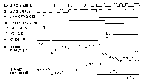
applied to circuits 151 that integrate signal over
l0 periods defined by an "Edge 1" control signal in a
circuit 153. Similarly, integrating circuits 155
receive the signal from circuit 137 and integrate it
over periods between pulses in an "Edge 2" control
circuit 157. The timing of the Edge 1 and Edge 2
signals, and thus the integration periods of the
respective integrators 151 and 155, is determined from
the estimated timing of the unknown A-code with which
both of the received L1 and L2 signals can be modulated.
Each of the integrating circuits 151 and 155
have two basic types of outputs. A first output of the
integrators 151 in a circuit 161 is a value of the
integration, and a second output in circuits 163 is its
sign. That sign is an estimate of the A-code as derived
from the L1 signal. Similarly, the integrator 155 has
an output in circuits 165 that corresponds with the
integration while its sign is outputed in circuit 167
and is an estimate of the modulating A-code during the
period of integration by the integrators 155, as derived
from the L2 signal. A mixer 169 in the L1 signal path
receives its integrated signal and mixes it with the A-
code estimate derived from the L2 signal. Similarly, a
mixing stage 171 in the L2 signal path mixes the A-code
estimate derived from the L1 signal with the signal in
circuits 165. Outputs of these mixing stages in
respective circuits 173 and 175 are then a signal that
has had the unknown A-code modulation .removed to a large
~ss~os
19
extent from both of the L1 and L2 signals, provided that
estimates of its timing made in generating the Edge 1
and Edge 2 integration time signals by the circuits have
been correct.
The periodic integrations of the Ll
accumulators 151 and L2 accumulators 155 are added
together by additional accumulators in summation
circuits 177. The results of the accumulations in the
integrators 151 and 155 are periodically transferred to
the summation circuits 177 through switches 179 and 181
that are operated by an "Add" control signal in a
circuit 183. The accumulation of these periodic
integrals generates the desired observables RO-R5 in
circuits 101 which the microprocessor uses to adjust the
phases of the carrier and code generators to cause them
to align with components of the received L1 and L2
signals. The circuits within a dashed box 185 and those
within a dashed box 187 are functional equivalents of
receiver circuits identified in Figures 5-19 with the
same reference numbers.
It has previously been described with respect
to Figure 4 that the A-code rate estimate derived from
each carrier signal, in circuits 163 and.167, are mixed
with the signals in respective mixers 169 and 171. Of
course, this is only necessary if the P-code in each of
the Ll and L2 signals is being modulated by the unknown
anti-spoofing A-code signal. Therefore, a switch 189 is
provided in the signal paths 163 and 167 to open in
response to the control signal Y in line 45 when the
satellite signal does not contain the anti-spoofing A-
code signal. There is obviously then no need to provide
an estimate of the unknown A-code.
CodeLRate Generation and Synchronization
Figures 6 and 7 illustrate in detail a
preferred code/rate generation and synchronization
20
circuit 111 combination as illustrated in the simplified
digital channel processor diagram of Figure 4 and the
more complete processor diagram of Figure 5. The
circuit of Figure 6 has three principal functions, among
others. One is to generate a receiver's replica of the
C/A-code contained in the L1 signal of the satellite
being monitored by the particular digital channel
processor of which the Figure 6 circuit is a part. The
second is to generate replicas of P-code, for both the
L1 and L2 signals of the satellite being monitored. The
third function is to generate an estimate of the rate of
the anti-spoofing A-code and develop from that signals
which time the integration period of the primary
accumulators 151 and 155.
Referring first to the generation of a C/A-
code, a generator 201 of the same code used by the
satellite being tracked responds to a clock signal from
a circuit 203 to generate in a line 205 such a C/A-code
digital signal. This signal repeats every one
millisecond. A second output line 207 of the generator
circuit 201 is asserted every one millisecond upon the
G1 shift register within the generator reaching its
epoch state of 1111111111. The rising edge of this
signal is detected by circuit 209 (Figure 7), to
generate the Clear signal in line 147 that has been
discussed previously with respect to Figure 4. The
Clear signal occurs every one millisecond in
synchronization with the locally-generated C/A-code in
line 205.
As is standard, the C/A-code is provided with
three different relative phases in lines 211, 213, and
215. The output of the generator 201 is passed through
two delaying circuits 217 and 219 in series to provide
a late C/A-code in line 213. The period of delay in
each of the circuits 217 and 219 is one-half of a C/A-
code cycle or chip. An early C/A-code is provided in
~~~.~.~~irl
21
line 211 that is outputted directly from the C/A-code
generator 201. A punctual C/A-code in line 215 has a
phase in between the early and late codes and is taken
from the junction intermediate of the two delay circuits
217 and 219. The relative phase of the C/A-code being
generated is controlled over the microprocessor control
bus 105 through the shifting circuit 203.
A P-code generator 221 outputs in line 223, in
response to a clock signal from circuits 225, the P-code
generated in the satellite whose signals are being
tracked. Rather than use a separate P-code generator
for each of the L1 and L2 signals, as is usually the
case, a single generator 221 is used but the phases of
the P-code applied to the L1 and L2 signals are
controlled by a digital delay line 227. A first tap 229
provides a P-code for mixing with the L1 signal. A
second tap 231 is provided as part of the delay line 227
to supply the P-code for mixing with the L2 signal. The
space between these taps 229 and 231 is due to the
different amount of phase delay experienced by the
different frequency L1 and L2 signals when passing
through the Earth's ionosphere.
The relative phases of these L1 and L2 P-code
signals are more finely adjusted, to a higher resolution
than practical by use of the delay line 227 itself, by
a phase interpolator 230 that is described below in
another section, with reference to Figures 15 and 16.
The result is a punctual L1 P-code signal in a line 231,
an early L1 P-code signal in line 233, and a late L1 P-
code signal in line 235. Similarly, a punctual L2 P-
code signal is generated in line 237, with an earlier
version appearing in line 239 and a later version
appearing in line 241. The early and late signals are
respectively shifted in time ahead and behind the
punctual signal by one-half the P-code cycle or chip.
The relative phases of the L1 and L2 P-code signals are
2~0~.0~~
22
coarsely shifted by commands from the microprocessor
over the control bus 105 to the delay line 227 in
effectively moving the positions of the taps 229 and
231, and more finely adjusted by the interpolator
circuits 230. Also, the phases of both the L1 and L2 P-
code signals can be shifted together using the P-code
shifter 225.
An A-code rate generator 251 generates a
signal in a line 253 that has a transition coincident
with an estimate of the end of each bit of the unknown
A-code. That signal is delayed by an adjustable digital
delay line 255 of the same type as the delay line 227
used in generating the L1 and L2 P-code. A tap 257
obtains such a signal for use in timing integration of
the L1 satellite signal, the result occurring in a line
258 at the output of the phase interpolator 230, a form
of this signal being shown in Figure 8(C). Similarly,
a second tap 259 is provided to adjust the relative
phase of the A-code rate signal for use in the L2 signal
processing and is more finely adjusted by the phase
interpolator circuits 230. An example of a phase
adjusted L1 A-code rate signal in line 260 is shown in
Figure 8 (D) . The L1 A-code rate signal in a line 258 is
applied to an edge detecting circuit 261 (Figure 7) to
develop the Edge 1 signal pulse in line 153 each time
the signal in the line 258 changes state, as shown in
Figure 8(E). Similarly, an edge detector circuit 263
produces the Edge 2 signal pulse in line 157 upon a
transition of the A-code rate signal in line 260, as
shown in Figure 8(F). A state machine 265 responds to
occurrence of both the Edge 1 and Edge 2 pulses to
generate the Add pulse in line 183, an example of which
is shown in Figure 8(G).
Since it is known that the period of each A
code cycle is approximately 20 P-code cycles, the A-code
rate generator 251 responds to a clock signal from the
23
same circuits 225 as does the P-code generator 221, but
generates a transition in output line 253 only once
every approximately 20 P-code cycles. It is further
believed that the anti-spoofing signal is generated in
synchronism with the P-code, so programmable
synchronization circuits 267 are provided to generate a
synchronizing pulse in a line 269 to the A-code rate
generator in response to detecting a particular state of
the X1A register of the P-code generator over lines 271.
That detected state can be, for example, the epoch state
of the X1A register, which is 001001001000.
In addition to the A-code rate generator 251
being synchronized with the P-code generator 221, the
taps 257 and 259 of the A-code rate delay line 255 are
adjusted along with the respective counterpart taps 229
and 231 of the P-code delay line 227. This further
maintains the A-code rate signals being generated in
complete synchronism with the P-code signals.
Figure 8(H) shows an example state of the L1
primary accumulators 151 (Figure 4). Its input signal
in circuit 135 is integrated for a time between
successive Edge 1 pulses. Similarly, the L2 primary
accumulators 155 integrate the signal in their input
circuit 137 between successive Edge 2 pulses, as
illustrated in Figure 8(T). The value of the
integration is passed on to the next stage and mixed
there with the sign of the integration from the primary
accumulator of the other channel, as discussed with
respect to the mixers 169 and 171 of Figure 4. It is
that sign that is an estimate of the A-code during the
interval between the edge pulses, and that is used to
remove its effect from the signals being processed. The
result of each such integration and mixing, when
effectively averaged over a number of such periods by
the secondary accumulators 187, mitigates the effect of
the unknown A-code modulation when the Edge 1 and Edge
24
2 pulses are synchronized with the ends of the A-code
cycles. That is, for the purpose of this integration,
the content of the code is not required but only an
approximation of its timing is desired. Although
optimum operation occurs when the Edge 1 and Edge 2
signals are generated exactly at the termination of each
A-code cycle of the received signals, it is satisfactory
if this is only approximately achieved, so long as the
A-code estimate is not in phase quadrature to the actual
code. Even if the actual A-code and its estimate
generated in the receiver are asynchronous, the system
operates acceptably, although with some degradation.
As stated above, it is known that the cycle
time of the A-code is equal to approximately 2o cycles
or chips of the P-code. It has been deduced that the A
code cycle time is not uniform, but rather repeats in a
pattern of a number M of A-code cycles or chips each
having a duration of A P-code cycles or chips, followed
by N A-code cycles that each are B number of P-code
cycles in length. It is desired to provide a A-code
rate generator 251 where the parameters A, M, B, N are
programmable over the microprocessor control bus 105.
The A-code rate sequence would repeat after A x M +
B x N cycles of the P-code clock. In order for this
sequence to be synchronous with the X1A register of the
P-code generator, A x N + B x M - 4092. This
programmability, along with the ability to synchronize
the A-code rate generator 251 with the P-code generator
221 (Figure 6), allows the rate of the A-code to be
adjusted to optimize the digital channel processor
operation.
Referring to Figure 9, an exemplary circuit
for the A-code rate generator 251 of Figure 6 is given
that is adjustable in the manner discussed above.
Registers 262, 264, 266 and 268 store, respectively, the
quantities A, B, M and N defined above. These registers
25
are loaded under the control of the microprocessor
system 41 over the system bus 105, The circuit of
counters, gates and flip-flops then repetitively
provides the bit pattern in an output 253 that matches
the timing of the anti-spoofing signal of the satellite
signals being processed.
With reference again to Figure 5, a more
detailed representation of a preferred digital channel
processor is given. Each of the L1 carrier generator
107 and L2 carrier generator 109 includes a circuit
shown in Figure 10. A numerically controlled oscillator
305 provides a relative phase output in circuits 307 in
response to a microprocessor command communicated over
the control bus 105. This relative phase is decoded by
circuits 309 to provide both cosine and sine functions.
A cosine output is represented as 311 or 313, depending
upon whether the circuit of Figure 10 is serving as the
L1 carrier generator 107 or L2 carrier generator 109 of
Figure 5. Similarly, a sine output provides signals in
the circuits 315 or 317 of Figure 5. A phase latch
circuit 319 periodically stores the output of the
numerically controlled oscillator 305 to provide a
signal in either of the lines 119 or 125 that gives the
oscillator's relativs phase.
Referring again to Figure 5, a mixing stage
115 receives those outputs from the L1 carrier generator
107 and mixes them with the quadrature L1 received
signals in circuits 25 to provide an output in circuits
117. The signal in a circuit portion 321 of the output
circuits 117 is labeled cos(~S~°~N~) to show the relatives
phase relationship between the phase ~S~ of the L1 P-code
carrier being received, and the phase r~N1 of the
numerically controlled oscillator 305 of the L1 carrier
generator 107. Similarly, a second output line 323
carries the signal that is labeled as sin(~S1-~N~). The
signals, in lines 321 and 323, can be seen to represent
26
differences between the relative phases of the carrier
of the L1 signal being received and that of 'the replica
of that carrier that is being generated within the
receiver in the Ll carrier generator 107. These signals
also have the C/A-code and P(Y)-code on them. The goal
of the system, of course, is to lock the locally
generated carrier in phase with that of the signal being
received from the satellite. When that is the case, the
phase difference (~s~-~N~) is zero, the cosine function
in line 321 then being one, and the sine of that
function in line 323 being zero. The use of these
quadrature functions permits simplified and rapid
locking of the carrier and code loops in the system.
The signals in the lines 321 and 323 provide this Ll
relative phase information to both the C/A-code
processor 141 and P(Y) code processor 185 described
below in another section, to obtain the observables T1-
T3 and RO-R5 that are used to lock the carrier and code
loops.
The mixer 121 performs the same function in
the L2 carrier path as does the mixer 115 in the L1
carrier path. One of the two outputs 123, in a line
325, is cos (~SZ-~NZ) , where cpsz is the P-code carrier
relative phase of the L2 signal being received, and $N2
is the relative phase of the numerically controlled
oscillator 305 that is provided as part of the L2
carrier generator 109. In a line 327 is the signal
sin ($SZ-~NZ) . The signals in the lines 325 and 327
provide L2 relative phase information to the P(Y) code
processor 185.
Receiver Adaptation to the Unknown Anti-Sboofina Si.anal
In order to adapt the receiver to the A-code
timing described above, either initially or because one
or more of the assumptions stated above is not correct,
circuits are provided as part of the receiver itself to
~4510~'~
27
appropriately align the A-code rate signal of the
generator 251 of Figure 9 with the received A-code in
conjunction with the locally generated P-code when an
actual satellite signal is being received that has the
anti-spoofing turned on.
These circuits include logic 501 of Figure 6
that detects from the circuit 271 a particular state of
the P-code generator X1A register as designated over the
control bus 105. In response to this state being
detected, a synchronizing pulse is issued in line 503 to
an inphase/midphase transition detector timing generator
505, an example of which is given in Figure 12. The
transition detector 505 is of a well known type and
generates three separate timing signals in circuits 507
that are related to an edge of the pulse in the circuit
503, thereby related in time to the occurrence of the P-
code generator 221 XlA register state to which the state
detection circuit 501 is set by the system.to respond.
These three signals are an early one in a line 509,
synchronous with that state, a mid ono in a line 511,
which is delayed by 10 P-code chips from the pulse in
line 503, and a late one in a line 513, delayed by 20 P
code chips. The duration of each of these three signals
is 20 P-code chips, equal to the approximate width of
the A-code bit.
The relative phases of these three signals are
adjusted by use of three separate digital delay lines,
shown in Figure 6 as a single delay line 515 for
simplicity, having output taps adjustable together,
indicated by a single tap 517. These taps are further
adjusted together with the L1 taps 229 and 257 of the
delay lines 227 and 255, respectively. The delay lines
provide a coarse phase adjustment of the early/mid/late
signals, which are more finely adjusted by the phase
interpolator 230, described hereinafter, to provide an
early inphase signal in line 519, a midphase signal in
2~~'1~~~
28
line 521 and a late inphase signal in line 523,
respectively.
With reference to Figure 5, it is noted that
these timing signals in lines 519, 521 and 523 are used
by a bit synchronizer 525 to develop an observable R6 in
circuits 527. An example bit synchronizer circuit is
given in Figure 13, receiving developed L1 signals in
lines 231 and 321 and mixing them in a mixer 529. When
the carrier and code loops are locked, the output of the
mixer 529 is a signal representing the received L1 P-
code signal with its carrier and P-code removed by
demodulation. This output signal represents the A-code
of the L1 signal, plus noise. Primary accumulators 531
and 533 integrate this result over periods defined by
logic 535 in response to the inphase/midphase timing
signal inputs in lines 519, 521 and 523. A secondary
accumulator 539 accumulates and averages a number of
such integrations that take place over a one .millisecond
interval, as defined by the clear signal in line 147.
When tracking the Y-code, even if the A-code
rate is asynchronous to the received A-code, the R6
observable provides an indication of how closely the
edges of the midphase signal in line 521 of the
transition detector are in phase quadrature to those of
the A-code in a satellite signal being received. The
level of R6 (on the y-axis) is shown by a curve 541 in
Figure 14 as a function of the P-code register X1A state
(indicated on the x-axis) that is programmed through
into the state detection logic 501.
When using this feature being described, the
receiver is connected to a directional antenna pointed
at a specific satellite. This antenna desirably has 20-
25 dB of gain over a 3 dB~ linearly polarized antenna.
An omni-directional antenna usually used when operating
the receiver will have insufficient gain for determining
the necessary bit transitions. The A-code rate
29
generator is then programmed to generate an A-code rate
that is asynchronous with the actual A-code rate of the
received signal. This causes a pseudo-random phase
relationship between the integration period of the
primary accumulators and the received A-code timing. It
is still possible to track the Y-code signals when the
A-code rate generator is asynchronous to the actual A-
code rate; however, some degradation in signal-to-noise
ratio results. The C/A-code is locked in the usual
manner. The Y-code is also locked as described in
Figure 20. When receiving an anti-spoofed signal from
the one satellite, the X1A register state loaded into
the state detect circuit 501 is varied and the resulting
R6 output is observed. Integration by the bit
synchronizer circuit 525 is performed for a period of
ten seconds for each such register state. This provides
one point on the curve of Figure 14. After one point is
obtained, the X1A register state loaded in the state
detect circuit 501 is changed and a new value of R6
determined to provide another point on the curve 541.
It is desired to determine the X1A register
states that correspond to the zero crossings of the
curve 541 (Figure 14) which have a positive going slope.
These are the P-code states where edges exist of the
unknown A-code modulated onto the L1 signal being
analyzed. Once the timing of these edges is determined,
values of A, B, M and N axe loaded into registers of the
A-code rats generator 251 (Figures 6 and 9) and a
beginning state is loaded into the state detect circuit
267 (Figure 6), in order that the A-code rate signal
generated in line 257 has edges at the same X1A register
states as determined for the actual signal.
Since there are 4092 states through which the
P-code generator X1A register cycles, this represents a
significant amount of computation. However, since it is
known that edges of the A-code occur at intervals of
2~~10~'~
approximately 2o P-code chips or x1A register states,
once a zero crossing with a positive slope of the curve
541 is determined, the next computation is performed by
advancing the X1A register state by about 20 counts to
5 look fox the next such zero crossing.
Phase Interpolator
The fine phase adjustments mentioned
previously are implemented by the phase interpolator 230
of Figure 6, an example implementation of which is given
10 in Figure 15, with a sample timing diagram thereof shown
in Figures 16(A)-(J). The relative phases of three sets
of signals are adjusted by the phase interpolator 230.
A section 543 finely adjusts the L1 and L2 P-code
signals from the delay line 227, another section 545 the
15 L1 and L2 A-code rate signals from the delay line 255,
and a third section 547 the early/mid/late signals from
the delay lines 515. All three of these sections
operate similarly. A final section 549 provides control
and timing signals to the other three sections. By
20 increasing in this manner the resolution to which
relative phases of various signals can be adjusted, a
receiver is provided with very high resolution without
the need to use extremely high clock speeds which are
impractical since the most commonly used circuit
25 technology cannot operate fast enough to provide the
same resolution as provided by the phase interpolation
technique of the present invention.
The specific implementation of the phase
interpolation technique executed by the circuit of
30 Figure 15 utilizes two of the system clock signals which
are close to each other in frequency. The 1.888 fo
clock in line 92, shown in Figure 16(B), and the 2 f0
clock in line 87, shown in Figure 16 (C) , are synchronous
with the 34 f0 clock illustrated in Figure 16(A), in a
manner previously described with respect to Figure 3.
2~~10~'~
31
The rising edges of each of the 1.888 f0 and 2 f0 clock
signals are utilized for various sampling, counting and
similar functions.
The control and timing section 549 of the
Figure 15 phase interpolator circuit utilizes a counter
551 and comparators 553 and 555 as principal components.
The 2 f0 clock signal is applied through a flip-flop
565, an output of which in a line 566 is a 1 f0 clock,
shown in Figure 16(D). The line 566 is an input to a
ZO second flip-flop 567 that is clocked with the 1.888 f0
cloak signal. An output of the flip-flop 567 is
provided as an input to a flip-flop 569. Outputs of the
flip-flops 567 to 569 are both applied to an exclusive
NOR gate 571, whose output in the line 554 is a clear
pulse illustrated in Figure 16(E). This clear pulse
occurs from the circuit of Figure 15 when two
consecutive samples of the 1 f0 clock in line 566 taken
by the rising edge of the 1.888 f0 clock in line 92, are
of the same polarity. This indicates that the clock
signal cycles of the 2 f0 and 1.888 f0 clocks at that
time are substantially aligned in phase. The clear
signal in line 554 then synchronously resets the counter
551. Figure 16(F) illustrates the states of the counter
551 which is clocked by the 1.888 f0 signal.
The state of the counter 551 is applied to two
comparators 553 and 555, which compare its count X with
respective reference counts Y1 and Y2, which are loaded
through the control bus 105. An output 556 of the
comparator 553 provides one input to an OR gate 557, a
second input of that gate being the clear signal from
line 554. An output in the line 561 of the OR gate 557
is a select signal of a type illustrated in Figure
16(J). A rising edge of the select signal, at a time tl
in Figure 16, for example, is coincident with a rising
edge of the clear pulse of Figure 16(E), which is one
input 554 to the OR gate 557. A falling edge of the
32
select signal of Figure 16(J) occurs at a time t2, when
the counter 551 is detected by the comparator 553 to
exceed the count Y1 that has been loaded in the
comparator 553. The timing of the falling edge t2 of
the select signal in line 561 is selectable by loading
a new quantity Y1 in the comparator 553, but its rising
edges are fixed in time with the periodic rising edge of
the clear pulses of Figure 16(E), which coincide with a
phase coincidence of the rising edges of the 1.888 f0
and 1 f0 clocks. .A similar select signal is generated
in a line 563 from a similarly operating comparator 555,
which also receives the output of the counter 551, and
an OR gate 559, but has a falling edge that is
adjustable in time independently of the select signal in
the line 561 by the loading of the control count Y2 in
the comparator 555. In this example, the select signal
in line 561 is used with L1 signals in the interpolator
circuit sections 543, 545 and 547, while the select
signal in the line 563 is used in those sections with L2
signals.
Using the phase adjustment of the L1 P-code in
line 229 as a example, this signal from its delay line
tap 229 (Figure 6) is applied to a series of four flip-
flop circuits 573, 575, 576 and 577 in a shift register
that is clocked by the 2 f0 signal in line 87. This
results in generating the punctual L1 P-code signal in
lines 579 and 580 with a phase difference between them
of one 2 f0 clock period, which turns out in this
example to be one-half the period or chip of the P-code.
One of these two signals is selected by a multiplexer
583 (switch) and presented at the output 231 in response
to the select signal in line 561. When the select
signal is high, such as occurs between times t1 and t2
of Figure 16, the multiplexer 583 connects the output
231 to the "delayed°° version of the L1 P-code signal
which exists in line 580. Conversely, when the select
33
signal is low, such as occurs between times t2 and t3 of
Figure 16, the multiplexes 583 connects its output 231
with an "undelayed" version of the signal in line 579.
Examples of these signals are also shown in
Figure 16. Figure 16(G) shows an example of the
undelayed signal in line 579, Figure 16(H) an example of
the delayed signal in line 580, and Figure 16(I) an
example of the desired punctual P-coda signal to be
generated in line 231 at the output of the multiplexes
583. It is important to note that, in general, the
signal generated at the output of multiplexes 583, in
line 231, does not have the same value as the desired
P-code phase; however, at all rising edges of the 1.888
f0 clock the output of this multiplexes assumes the same
values as the desired P-code signal. The values
determined for the desired signal are thus only those
coincident with the rising edges of the 1.888 f0 clock.
Thus, the signal in the line 258 is finely.adjusted in
phase as a result of selecting the threshold count Y1 to
be loaded in the comparator 553. The value of Y1
determines the count corresponding to the time t2 where
the select signal has its falling edge and switches the
desired signal from following the delayed signal to
following the undelayed signal.
The multiplexes 583 is caused to
simultaneously switch connection of the early L1 P-code
line 233 between undelayed and delayed versions in lines
578 and 579. Similarly, the late L1 P-code line 235 is
switched between lines 580 (undelayed) and 581
(delayed).
The same technique is used to adjust the phase
of the L2 P-code signals of lines 237, 239 and 241,
except that the L2 select signal in line 563 is
connected to switch its multiplexes in providing output
signals in the line 231.
34
In a similar manner, the L1 A-code rate signal
in the line 257 is phase adjusted, using a series
connection of three flip-flop stages 601, 603, and 605.
A multiplexes 611 selects, in response to the L1
switching signal in line 561, either an undelayed
version of that signal in a line 607 or a delayed
version in a line 609. The L2 A-code rate signal in the
line 259 is similarly processed, except that its
multiplexes switches between the undelayed and delayed
versions of that signal in response to the L2 switching
signal in line 563.
The same technique is also used in
interpolator section 547 with each of the signals in
lines 509, 511 and 513, all of which have their
multiplexers switched by the L1 select signal in line
561.
It can thus be seen that the phase
interpolator 230 of Figure 15 operates to. adjust the
phases of its output signals relative to those of its
corresponding input signals by control of the counts Y1
(for the L1 signals) and Y2 (for the L2 signals). Each
of these counts determines the time t2 (Figure 16) at
which samples of desired output signals cease being
taken from delayed versions of input signals and instead
begin to be taken from undelayed versions. This
switching causes no discontinuity since it is being
implemented as part of a sampled data system. When the
source of the desired output signal samples is switched
back to the delayed input signal, such as at time tl,
the leading edges of the 1.888 f0 and 2 f0 clock signals
are coincident. After one cycle of each clock signal,
the 1.888 f0 leading edge occurs a time ~t after the
leading edge of the 2 f0 signal, as indicated in Figure
16. After n number of clock cycles, this difference is
T=nit. The switching point t2 is selected to occur when
the value of T is equal to the delay of the desired
2~~~~~'~
output signal with respect to the undelayed input
signal, at which point the undelayed signal becomes its
source instead of the delayed signal. The technique
operates to provide an adjustable average phase of the
5 output signals over the period of the counter 551.
The C/A Code and P-Code Processors
The C/A-coda processor 141 of Figure 5, shown
in its components 143 and 145 in the simplified diagram
of Figure 4, is shown in more detail in Figure 11. The
10 mixing stage 143 has as a purpose to mix off the C/A-
code on the L1 signal and the correlators 145 have as a
purpose to provide signals to indicate when the locally
generated C/A-code signal is in phase with that on a
received L1 signal being processed. Within the mixing
15 stage 143 are individual mixing circuits 331 and 333
that provide outputs to respective correlator circuits
343 and 345. The circuits 331 and 333 mix off the
nominal C/A-code of each of the signals in lines 321 and
323 from the previous mixing stage 115. Another mixing
20 stage 335 mixes off the early C/A-code from the signal
in line 323, and the mixer 337 mixes off the late C/A-
code from the signal in the line 323. The outputs of
the mixers 335 and 337 are combined by an adding circuit
339, its output being applied to a correlator 341.
25 It can be seen that the integration performed
by the correlators 343 and 345 minimizes the T1 signal,
maximizes the T2 signal, and minimizes the T3 signal
when the locally generated C/A-code is in phase with
that of the satellite signal being tracked. This is
30 then used by the microprocessor system 41 to control the
phase of the C/A-code generator 21 to bring about such
an alignment. The correlators 343, 345 and 341 operate
to integrate their respective inputs over the same time
period controlled by the Clear timing signal in line
35 147.
36
Referring to Figure 17, an implementation of
the P(Y) code processing circuits 185 of Figures 4 and
is given in some detail. The mixers 127 and 129 of
Figure 4 are shown in expanded detail in Figure 11, as
5 are the primary accumulating circuits 151 and 155. The
mixing circuit 127 has as a primary function to mix off
of the L1 signal output of the prior mixer 115 the L1 P-
code signal. The mixing circuit 127 includes four
individual mixers 351, 353, 355, and 357, connected as
indicated in Figure 17. An addition circuit 359 is also
included. The primary function of the mixing circuits
129 is to mix off the P-code from the L2 signal output
of the mixer 121. The mixing circuit 129 is generally
of the same structure as that of the circuit 127, but is
connected to corresponding L2 signals rather than L1
signals.
The primary accumulators 151 of Figure 4
include three individual accumulator circuits 361, 363
and 365 of Figure 17 which function to integrate, over
periods between Edge 1 pulses in line 153, the
respective outputs of the mixer 351, mixer 353 and
addition circuit 359. Similarly, the primary
accumulators 155 of Figure 4 include three individual
accumulator circuits 367, 369 and 371 of Figure 17 which
integrate their respective inputs over time periods
between Edge 2 pulses in line 157. The structure of
each of the six accumulator circuits so shown in Figure
17 is given in Figure 18.
A second portion of the P(Y)-code processing
circuits 185 of Figure 5, functionally shown within
dotted outline 187 of Figure 4, is also given in Figure
17. Six identical summation circuits 401, 403, 405,
407, 409 and 411 receive the outputs of the primary
accumulators 361-371 in the specific combinations shown.
The circuit structure of each of these summation
circuits is given in Figure 19. After correlating with
20f~100'l
37
the appropriate cods and carrier replicas, the noise
components which affect the observable outputs are zero
mean; therefore, the time average of the observable
outputs RO-R5 are given by the following expressions:
(.RO)~ f PZ ( t) ' P1 ( t-T1) ' sin (t~s1-~NI) ' ALI° ALa° dt
(RZ)~ f PZ ( t) ' Pl ( t-T1) ' cos (~s1-~NZ) ' ALx' ALa° dt
~R2)~f {PZ{t)' E1(t-T1)-PZ{t)' L1{t-T1))
C O S { t~s1 'o'NI ) °'~L1 '~L2 ° d t
(R3)«~P2 ( t) ' P2 ( t-T2) ' sin (~S2-'o'N2) ° AL2° ALI' dt
(R4)« f P2 { t) ' P2 ( t-T2) ' COS (~,s2 ~N2) ° '~L2°
'AL1° dt
lLC2)« f {P2 { t) ' E2 { t-T2) -P2 ( t) ' L2 { t-T2) )
COS {~S2 'o'N2) '~L2AL2° dt
where:
A~~ = Anti-Spoof bit modulating L1 P-code;
ADZ = Anti-Spoof bit modulating L2 P-code;
A~~ = estimate of Anti-Spoof bit modulating L1 P-coda
(line 163);
A ~Z = estimate of Anti-Spoof bit modulating L2 P-code
(line 167);
E1 = early estimate of received L1 P-code (line 233);
E2 = early estimate of received L2 P-code (line 239);
L1 = late estimate of received L1 P-code (line 235);
L2 = late estimate of received L2 P-code (line 241);
P1 = received L1 P-code;
P2 = received L2 P-code;
2a~10~~r
38
P1 = punctual estimate of received L1 P-code (line 231);
P2 = punctual estimate of received L2 P-code (line 237);
= NCO 305 phase;
- satellite carrier phase;
T~ = L1 P-code phase offset;
T2 = L2 P-code phase offset; and
< > denotes time average.
The integration periods of each of the summation
circuits 401-411, as indicated by the above expressions,
are intervals between successive clear pulses in the
control line 147. That is, the integration period is
the one millisecond repetition period of the C/A-code
epoch. Integration is performed in the microprocessor
system 41 over a period of 100 milliseconds.
Carrier and Code Loob Locking Processing
Referring to Figure 20, a preferred technique
is outlined for adjusting and locking the carrier and
code generators into phase with the carriers and code of
the satellite signals being processed. In a first step
413, the numerically controlled oscillator "N1" 305 in
the L1 carrier 107, and the C/A-shifter 203, are
adjusted in order to maximize the signal T2 and minimize
the signals T1 and T3 from the C/A-code processor 141.
When this occurs, the nominal C/A-code in line 215 is
then known to be in phase with that of the L1 signal
being processed. This provides an unambiguous reference
for the L1 C/A-code carrier, and thus also for the L1 P-
code carrier that is displaced ninety degrees from it.
When the L1 carrier loop is thus locked, the quantity
(~S~-~N~) of the equations given above, which represents
the phase difference between the L1 carrier and the L1
NCO, is approximately equal to zero.
A next step 415 is for the microprocessor to
adjust the L1 arid L2 P-code delay line taps 229 and 231
2Q6~.fl~a'l
39
(Figure 6) and load the L1 and L2 comparators 553 and
555 of the interpolator 230 (Figure 15) in order to
maximize the quantities (R3)Z a- (R4)2. As previously
discussed, adjustment of the P-code delay line 227
causes a corresponding adjustment of the L2 tap 259 of
the A-code rate delay line 255. This adjustment
approximates synchronization of the locally generated P-
code with that of the signals being received and
processed. The locally generated P-code signals are not
yet locked in phase with those of the received signals
but are close enough to being in phase so that the L2
carrier loop can be locked.
Since the value of the received A-code bit is
unknown, there exists a phase ambiguity in the L2
carrier because this A-code bit modulates the phase of
the L2 carrier. However, the A-code bit affects both
the L1 and L2 signals, and the phase of the L1 carrier
is known because it is determined when tracking the C/A-
code. This allows determination of the phase of the L2
carrier without ambiguity. Therefore a next step 417
adjusts the numerically controlled oscillator "Id2" 305
of the L2 carrier generator 109 in order to minimize the
R3 output of the secondary accumulators while
maintaining R1 and/or R4 positive. Once this is
accomplished, the locally generated L2 carrier is locked
in phase with that of the satellite signal being
received, without a one-half L2 carrier cycle ambiguity
that is characteristic of prior art techniques. When
the L2 carrier loop is thus locked, the quantity (~S2-
cpN2) of the equations given above is approximately equal
to zero. The phase "~PZ°° output in line 125 of Figures
4 and 5 then provides that relative phase quantity.
In a step 419, the L2 P-code delay line tap
231 (Figure 6) is again adjusted, and the count set in
the L2 comparator 555 (Figure 15) of the interpolator
selected, in order to minimize the signal level R5.
40
Once this is accomplished, the punctual L2 P-code signal
in line 237 is then phase locked with the P-code
received on the L2 signal being processed.
Similarly, in a next step 421, the L1 P-code
delay line tap 229 (Figure 6) and the count set in the
Ll comparator 553 (Figure 15) of the interpolator are
adjusted to minimized the quantity R2. When this is
accomplished, the L1 punctual P-code signal in line 231
is in phase with that being received on the L1 signal
being processed.
Being able to lock the P-code loops on both
the L1 and L2 signals, even when modulated by the A-
code, is a significant advance. Being able to
demodulate the signal with these P-code replicas is of
15 considerable advantage. Nat only can the carrier phases
and ~P2, indicated in a step 423, be determined with
more precision, the ability to provide the Ll and L2
signal P-code relative phases is also of considerable
utility.
It will be noted that the selection of the
quantities RO-R5 expressed above and the technique of
locking the code and carrier loops overcomes a potential
error in determining the carrier phases. Each of the
carrier loops can be locked by adjusting the phase of
their respective NCOs 305 (Figure 10) to either of two
relative phases that are 180 degrees apart. That is,
there are two values of relat-ive phase which can be
loaded into the NCOs 305 of each of the carrier
generators 107 and 109 (Figure 5) that will lock their
respective loops but only one of these values is in
phase with their respective L1 and L2 signal carriers
and the other value is out of phase by 180 degrees. By
first locking onto the L1 signal C/A-code, in step 413,
which is not affected by the unknown A-code, the L1
signal C/A-code carrier is known without uncertainty.
The L1 signal P-code phase is then also known with
41
certainty, since it differs therefrom by ninety degrees.
The A-code estimate A~~ derived from the Ll signal is
also then known to have the correct sign. Therefore,
adjustment of the various parameters to minimize the
5 quantity R3 in the step 417 (Figure 20) will result in
substantially equaling ~SZ without ambiguity or
uncertainty. The phase values ~P~ and cpPZ are then
similarly certain and unambiguous.
Although the above method works when the
telemetry data on the L2 signal is present, it is
possible to multiply the values of RO-R6 by the sign of
the received telemetry bit extracted from the C/A°code
to allow operation when the data stream on the L2
carrier is turned off.
Although the various aspects of the present
invention have been described as implemented in a
preferred embodiment, it will be understood that the
invention is entitled to protection within the full
scope of the appended claims.