Note: Descriptions are shown in the official language in which they were submitted.
FJ-8991
- 1 - 20617~1~
VIDEO SIGNAL SYNTHESIZING SYSTEM FOR SYNTHESIZING
SYSTEM'S OWN SIGNAL AND EXTERNAL SIGNAL
BACKGROUND OF THE INVENTION
l. Field of the invention
The present invention relates to a video~signal
synthesizing system, and more particularly to a video
signal synthesizing system for synthesizing the system's
own video signal such as an analog video signal,
digital image data, encoded, compressed image data and
so on and external signals such as character signals
from other image processors.
2. Description of the Related Art
As inexpensive high-speed circuits such as ISDNs
are popularized and as semiconductor technology and
image compression technology improve, multimedia
transmission and display devices that can transmit
images of picture level, characters, and graphics are
realized. In these multimedia transmission and display
devices, synthesizing images from different image
devices such as character devices and graphic devices
can present various kinds of screen services to greatly
expand the functions of image processors.
The system for synthesizing system's inner video
signal or signals and video signals from external video
signal generating devices usually comprises an analog-
to-digital (A/D) converter and a memory for inner video
signal, an A/D converter and a memory for external
video signal, a memory for synthesizing inner and
external video signals, a digital-to-analog (D/A)
converter, a display, and so on. In this system, an
analog video signal generated from a system's own
apparatus (the inner video signal) is once converted
into a digital signal by the A/D converter and stored in
the memory, and an analog video signal from an external
apparatus (the external video signal) is also converted
- 2 - 20~1700
into a digital signal by the A/D converter and stored
in the memory respectively.
The digital video signals stored in the memories
are synthesized by the synthesizing memory and
converted again into an analog signal by the D/A
converter. The synthesized video signal is displayed
on the display.
In this way, the external video signal from the
external video devices and at least one internal video
signal are converted into digital signals and stored in
the two video memories respectively, and then
synthesized in a digital area. Accordingly, this system
requires memories for each signal and a synthesizing
memory, thereby increasing the cost.
In addition, it is obvious that digitizing the
analog video signals and then converting the digital
signal into an analog signal again may cause
(quantization distortion and thereby reduce accuracy.
SUMMARY OF THE INVENTION
The object of the present invention is to provide
a video signal synthesizing system that can synthesize
video signals from the system's own device and from an
external image processor as they are in analog form and
decrease the number of memories thereby minimizing
quantization distortion.
According to one aspect of the present invention,
an external video signal from the external image
processor such as a personal computer is transferred to
the video signal level changing portion, which changes
the dynamic range of the signal to be equal to the
dynamic range of the inner video signal generated by
the system's own apparatus. If the brightness of the
external video signal is too bright or dim, the
brightness is balanced with respect to that of the inner
video signal.
The synchronous signal transferred from the
external image processor is provided to the PLL portion,
_ 3 _ 2~Sl~D~
which synchronizes the synchronous signal of the inner
video signal with the externally transmitted synchronous
signal. After the synchronous signals are equalized,
the inner video signal is digitized and stored in the
memory. Then, the inner video signal provided by the
memory is converted into an analog signal, and added to
the external video signal transmitted from the external
image processor in accordance with the synchronous
signal. Added video signals are amplified and displayed
on the display.
According to another aspect of the present
invention, a plurality of analog inner video signals
are digitized and added before the addition of the
external analog video signal, and stored in the memory.
Then the added inner video signal provided by the
memory is converted into an analog signal, added to the
external video signal in accordance with the synchronous
signal. Added video signals are amplified and
displayed on the display.
In this way, the invention rea'izes an addition of
an analog video signal from the system's own device and
an analog video signal from an external image processor
thereby decreasing the number of memories and
minimizing quantization distortion.
BRIEF DESCRIPTION OF THE DRAWINGS
The present invention will be more clearly
understood from the description as set forth below with
reference to the accompanying drawings, wherein:
Fig. 1 is a prior art block circuit diagram of
a basic video signal synthesizing system;
Fig. 2 is a prior art block circuit diagram of
a video signal synthesizing system having a plurality
of inner video sources to be synthesized other than an
external video source;
Fig. 3 is a basic block circuit diagram of a
video signal synthesizing system according to one
embodiment of the present invention;
- 4 - ~ 7 ~ ~
Fig. 4 is a detailed block circuit diagram of
the video signal synthesizing system in Fig. 3;
Fig. 5 is a detailed block circuit diagram
showing an essential part of the video signal
synthesizing system in Fig. 4;
Fig. 6 is a basic block circuit diagram of a
video signal synthesizing system according to another
embodiment of the present invention; and
Fig. 7A and 7B are a detailed block circuit
diagram showing an essential part of the video signal
synthesizing system in Fig. 6.
DESCRIPTION OF THE PREFERRED EMBODIMENTS
Before describing the preferred embodiments, an
explanation will be given of the conventional video
signal synthesizing system shown in Figs. 1 and 2.
Figure 1 shows a conventional video signal
synthesizing system for synthesizing video signals from
the system's own apparatus and from external video
input apparatus. The system comprises analog-to-digital
(A/D) converters 100 and 103, memories 101 and 104, a
video signal level changing portion 102, a synthesizing
memory 105, a digital-to-analog (D/A) converter 10, a
display driver 20, a display 30, etc. An internal
analog video signal from a system's own apparatus is
converted into a digital signal by the A/D converter
100 and stored in the memory 101. An external analog
video signal from an external apparatus is converted
into a digital signal by the A/D converter 103 after
the adjustment of the signal level by the video signal
level changing portion 102 and stored in the memory 103.
The digital video signals stored in the memories
101 and 104 are synthesized by the synthesizing memory
105 and converted again into an analog signal by the D/A
converter 10. The synthesized video signal is
displayed on the display 30.
The conventional video signal synthesizing system
having the above-mentioned arrangements have the
- 5 - 20617Q0
following problems:
(1) The internal and external video signals are stored
in the built-in video memories 101 and 104 and
synthesized in a digital area thereby requiring a
synthesizing memory 105 and increasing the cost; and
(2) It is obvious that double conversion of the analog
video signals from analog to digital and digital to
analog may cause quantization distortion and thereby
reduce accuracy.
Figure 2 shows another conventional video signal
synthesizing system for synthesizing three inner video
signals from a system's own device and external video
signals from an external video input apparatus. In Fig.
2, the components used in Fig. 1 are assigned the same
reference numerals. The system comprises A/D converters
103, 210, 220, and 230, memories (VRAM : Video Random
Access Memory) 104, 211, 221, and 231, VRAM control
circuits 204, 212, 222, and 232, a video signal level
changing portion 102, a synthesizing memory 205, a D/A
converter 10, a display driver 20, a display 30, timing
control circuit 200, etc.
Three kinds of internal analog video signals
(video/image data #1-#3) from a system's own apparatus
are converted into digital signals by the A/D converters
210, 220, and 230 and stored in the memories 211, 221,
and 231 with the control of VRAM control circuits 212,
222, and 232. An external analog video signal from an
external apparatus is converted into a digital signal by
the A/D converter 103 after the adjustment of the
signal level by the video signal level changing portion
102 and stored in the memory 104 with the control of
VRAM control circuits 204.
The digital video signals stored in the memories
104, 211, 221, and 231 are synthesized by the
synthesizing memory 205 and converted again into an
analog signal by the D/A converter 10. The synthesized
video signal is displayed on the display 30. The VRAM
- 6
20G17Q0
control circuits 204, 212, 222, and 232 and the
synthesizing memory 205 is operated by the timing
information transmitted from the-timing control circuit
200. The operation of the video signal synthesizing
system of Fig. 2 will be explained hereinafter in
detail.
The memories 211, 221, and 231 used for the system
in Fig. 2 are required to have a high-speed read/write
function to follow a display speed, a function of
equally handling a plurality of image data input sources,
and a function of expressing image data with picture-
level colors (for example, eight bits each for R, G,
and B for presenting 16.7 million colors).
To achieve this, a conventional system shown in
Fig. 2 employs three memories (VRAMs) 211, 221, and 231
for each video/image data #1-#3 from a system's own
apparatus respectively, and an image synthesizing
circuit 205 for synthesizing video signals provided by
the memories 211, 221, and 231.
For example, the video/image data #l is a signal
from a video camera, the video/image data #2 is a
signal from a character input unit, the video/image
data #3 is a signal from a graphic input unit, and the
external signal is a signal from another character
generating device. Digital video signals from the A/D
converters 103, 210, 220, and 230 are passed through
write buses 90, 110, 120, and 130, and temporarily
stored in the VRAMs 104, 210, 220, and 230, respectively.
The VRAM control circuits 204, 212, 222, and 232
provide read/write control signals for controlling
read/write operations.
Signals read out of the VRAMs 104, 211, 221, and
231 are passed through display buses 91, 111, 121, and
131, and synthesized in the image synthesizing circuit
(synthesizing memory) 205. At this time, a timing
control circuit 200 provides the VRAM control circuits
204, 212, 222, and 232 and the image synthesizing
- 7 - 2~6~OD
circuit 205 with VRAM read timing information and
synthesis timing information.
The synthesized image from the image synthesizing
circuit 205 is converted into an analog signal by a D/A
converter 10 and displayed on a display 30 driven by the
driver 20.
In this sort of distributed control type video
signal synthesizing system shown in Fig. 2, each of the
lines for the video/image data #1-#3 has a VRAM, bus,
and VRAM control circuit, and data is read out of the
respective VRAMs. Namely, this system requires a
plurality of large scale VRAMs. In addition, the
system requires a plurality of image buses each having
a wide width (in the example of Fig. 2, each bus
comprises 24 lines) to complicate circuit patterns. To
read and synthesize a plurality of data from the VRAMs
and produce a single display plane according to the
synthesized data, read timing of the VRAMs must be
completely equalized. This sort of timing control is
difficult. For example, a timing control circuit must
be provided to control the timing of all of the VRAM
control circuits.
Use of the conventional system increases the
circuit scale, complicates the circuit arrangement, and
therefore, is unsuitable for small desktop size
apparatuses.
A first embodiment of the present invention will
be explained with reference to Figs. 3, 4, and 5. In
Figs. 3, 4, and 5, similar components as used in Fig. 1
are assigned the same reference numerals.
Figure 3 shows a basic block circuit diagram of a
video signal synthesizing system according to a first
embodiment of the present invention. The system
comprises an A/D converter 100, memory 101, a video
signal level changing portion 102, D/A converter 300,
an analog and video signals adding amplifier 40, a
display driver 20, a display 30, etc. An internal
- 8 - 20~17Q0
analog video signal from a system's own apparatus is
once converted into a digital signal by the A/D
converter 100 and stored in the memory 101. The digital
video signals stored in the memory 101 are input to the
analog and video signals adding amplifier 40.
An external analog video signal from an external
apparatus is adjusted to the signal level by the video
signal level changing portion 102 and then input to the
analog and video signals adding amplifier 40 without
being converted into a digital signal.
The analog video signals input to the analog and
video signals adding amplifier 40 are synthesized
hereby and the synthesized video signal is displayed on
the display 30 through the driver 20.
In comparing the video signal synthesizing system
in Fig. 3 with the conventional video signal
synthesizing system in Fig. 1, it is clearly understood
that the construction of the video signal synthesizing
system according to the present invention is simple,
because there is no A/D converter and memory for the
external video signal and synthesizing memory.
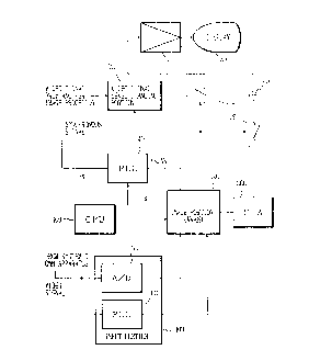
Figure 4 is a block diagram showing the
construction of the first embodiment of the present
invention, and Fig. 5 a detailed view showing an
essential part of the embodiment.
To achieve the previously described object, the
present invention shown in Fig. 4 arranges an input
portion 403, a CPU 400, an image portion (VRA~) 101, a
D/A converter 300, a video signal level changing
portion 102, analog switches 404 and 405, an analog
video signals adding amplifier 40, a driver 20, a PLL
(Phase Locked Loop) portion 401, display 30, etc. The
input portion 403 comprises an A/D converter 100, a PLL
portion 402, etc.
The input portion 403 receives an internal video
signal transmitted from a system's own video apparatus
such as a television camera. The signal is converted
20617Q0
into a digital signal by the A/D converter 100. A
synchronous signal contained in the received video
signal is transferred to the PLL portion 402, which
provides the image portion 101 with the synchronous
signal (for horizontal and vertical synchronization). A
frame memory in the image portion 101 stores the video
signal from the system's own apparatus.
An external video signal from an external image
processor such as a personal computer is provided to the
image signal level changing portion 102, and a
synchronous signal contained in the video signal is
supplied to the PLL portion 401.
The video signal level changing portion 102
adjusts the dynamic range of the video signal from the
external image processor to be equal to the dynamic
range of the image signal from the system's own
apparatus. If the input image signal is too bright or
dim, the image signal level changing portion adjusts the
same to the brightness of the image signal from the
system's own apparatus.
The PLL portion 401 adjusts the system's own
synchronous signal to the synchronous signal from the
external image processor.
The operation of the video signal synthesizing
system of Fig. 4 will be explained hereinafter in
detail.
In Fig. 4, numeral 403 denotes an input portion
for receiving a video signal and a synchronous signal
from a system's own video apparatus such as a television
camera. The video signal is converted into a digital
signal by an A/D converter 100, and the synchronous
signal is provided to a PLL portion 402. According to
the synchronous signal, an image portion 101 carries
out a control operation.
Numeral 400 denotes a CPU, which wholly controls
the image processing system.
Numeral 101 denotes the image portion, which
lO- 2~5170~
provides switching control signals to analog switches
404 and 407 according to instructions from the CPU 400.
The image portion has a memory for storing the video
signal from the system's own video apparatus.
Numeral 102 denotes a video signal level changing
portion, which equalizes the reference levels of analog
signals to be added. If the video signal from the
system's own video apparatus has intensity levels from
0 to 255 like a natural image, and if the video signal
from the external image processor such as a personal
computer has intensity levels from 0 to 15, these video
signals will not be correctly added to each other with a
simple analog adding operation. An intermediate level
128 of the 256 intensity levels and an intermediate
level 8 of the 16 intensity levels must be adjusted to
each other, and upper and lower intensities around the
intermediate levels must be balanced. This adjustment
may be done according to intensity levels derived from
the input signals. When the input signal from the
external image processor is too bright or dim, it may
be adjusted by changing to a proper intensity level.
Numerals 404 and 405 denote analog switches,
respectively. According to switching signals provided
by the image portion 101, the analog switch 404 alone,
or the analog switch 405 alone, or both of them may be
turned ON or OFF. When synthesizing and displaying the
video signal from the system's own apparatus and the
video signal from the external image processor, both
the analog switches 404 and 405 are turned ON. When one
of the signals is to be displayed, one of the analog
switches 404 and 405 corresponding to the signal to be
displayed is turned ON.
The analog video signals adding amplifier 40 for
adding the analog signals transmitted through the
analog switches 404 and 405 to each other comprises a
broad-band operational amplifier 41 and resistors R1 to
R5, as shown in Fig. 4. The operational amplifier 41
11- 2D~170D
is used with, for example, a non-inverting input, and
independently perform adding, amplifying, and driving
functions.
Numeral 401 denotes a PLL portion, which compares
the phase of a synchronous signal (a horizontal
synchronous signal) to be transmitted with the video
signal provided by the external image processor with
the phase of a horizontal synchronous signal from the
system's own image processor, and synchronizes these
signals with each other. In this way, this arrangement
synchronizes both signals with each other.
As shown in Fig. 5, the input video signal from
the external image processor is actually provided to an
interface 500, and the video signal is subjected to an
impedance matching process in a Z matching portion 112
and provided to the video signal level changing portion
102, which adjusts the level of the video signal.
At this moment, the level is set according to
information related to the external image processor.
For example, if the signal from the external image
processor is classified into four levels, the CPU 400
provides, automatically according to the video signal
level setting information or based on a keyboard input,
a 2-bit control signal to properly set the level.
The level-adjusted video signal is clamped by a
clamping portion 132 and transferred to the analog
switch 404 through a buffer 142. On the other hand, a
video signal from the image portion 101 is converted
into an analog signal by the D/A converter 300, clamped
by a clamping portion 501, and transferred to the
analog switch 405 through a buffer 502. These signals
are synthesized in the analog video signal adding
amplifier 40, and the synthesized signal is displayed on
the display 30 through the driver 20.
In this way, the present invention does not simply
add analog signals to each other but changes the level
of the external video signal provided by the external
- 12- 20617Q~
image processor and adds it to another analog inner
video signal. The the video signal synthesizing system
according to the present invention is very useful when
the inner video signal is a motion picture image and
the external video signal is a character image or vice
versa.
Due to the switches 404 and 405, the invention can
display not only a synthesized image but also images
provided by the external image processor and the
system's own image portion independently of each other.
The PLL portion may be modified according to a display
frequency of the external image processor. This
enables the system to easily accept other kinds of
external apparatuses.
The above-described embodiment can synthesize
external analog signals without converting them into
digital signals, so that circuits for converting the
signals are not needed, and quantization errors are
eliminated. In addition, various kinds of video signals
from external image processors can be synthesized with
the internal video signals by applying the above-
described embodiment.
A second embodiment of the present invention will
be explained with reference to Figs. 6 and 7. In Figs. 6
and 5, similar components as used in Fig. 2 are
assigned the same reference numerals.
Figure 6 is a block diagram showing the
construction of the second embodiment of the present
invention, and Fig. 7 a detailed view showing an
essential part of the embodiment. In the second
embodiment, the video signal synthesizing system has a
plurality of inner video signal sources, such as three
inner video signals from the system's own device, and
synthesizes them with one external video signal from an
external video input apparatus.
To achieve the previously described object in the
second embodiment, a VRAM controlling system that can
- 13- 20617Q0
materialize a compact multimedia image communication
terminal with a simple arrangement of a VRAM, an image
bus, and a VRAM control circuit, which has to be
arranged for each usage (for each input/output
interface) according to the prior art, and without
spoiling necessary functions is required.
Unlike the prior art that arranges VRAMs, image
buses, and VRAM control circuits for video and image
input sources respectively, and permits the video and
image input sources separate access to the VRAMs, the
invention considers the following points in achieving its
object:
(1) When actually displaying data, an image data
from only one VRAM is needed, and at a certain moment
only one VRAM is accessed;
(2) VRAMs are accessed for displaying images
therefrom or for writing images therein. During the
display access, all VRAMs must be ready (even if any one
of the VRAMs is unselected as a display plane, this
VRAM alone cannot be put in a write mode); and
(3) The display access must be continuously
carried out in time series. The access frequency under
a write mode is small (discrete) compared with that
under a display mode.
The invention arranges, as shown in Fig. 6, an
image portion (VRAM) 101, a video signal level changing
portion 102, a VRAM control circuit 202, a D/A
converter 300, analog switches 404 and 405, an analog
video signals adding amplifier 40, a driver 20, display
30 such as a CRT monitor, a master device 600, slave
devices 610, 620, and 630, an address selector 640, and
a converter 650. The master device 600 serves as a
master controller for collectively managing the control
right of the VRAM 101. The master device 600 controls
other video and image input sources, i.e., slave
devices 610, 620, and 630. Under the control of the
master device 600, the slave devices 610, 620, and 630
- 14- 2~17QO
share a single VRAM 101. Namely, the invention can
constitute a system with the VRAM 101, an image bus 80,
and a VRAM control circuit 202. Compared with the
distributed control system of Fig. 2, the invention
realizes a centralized control system.
The address selector 640 selects a slave device
610, 620, or 630 that has issued a bus request or the
master device 600 according to a selection signal
provided by the master device 600, and provides an
address.
The VRAM 101 may be formed in two layers (two
pixels being read each time in horizontal scanning) or
four layers (four pixels being read each time in
horizontal scanning) depending on a display purpose.
The converter 650 carries out an address output
conversion and a read/write control signal output
conversion according to the two or four layers.
In Fig. 6, the master device 600 has a read/write
control right of the VRAM 101, and the slave devices 610
to 630 are controlled by the master device 600 when
accessing the VRAM 101.
During the display mode, the master device 600
gives no reply to any one of the slave devices 610 to
630 that have issued a bus request signal, and
continues a display operation according to VRAM read
signals and addresses produced by the master device 600
Namely, the master device 600 exclusively uses the
image bus 80.
3uring the write mode, the master device 600
provides a reply to any one of the slave devices 610,
620, or 630 that have issued a bus request signal and
allocates a right to use the bus 80 to the slave device
610, 620, or 630. The slave device 610, 620, or 630
that has received the reply sends information, such as a
write address and write data peculiar to the slave
device, to the address selector 640 and bus 80.
The master device 600 provides the address
- 15- 2~S17~
selector 640 with a common signal such as a read/write
signal related to the VRAM 101 and a selection signal
corresponding to the slave device 610, 620, or 630 to
which the right to use the bus 80 has been given. The
VRAM 101 is then accessed according to the address
provided by the slave device 610, 620, or 630. At this
moment, the VRAM 101 operates as an exclusive memory for
the slave device having the bus using right.
Image data may be supplied in different formats
such as two- and four-layer formats depending on images
handled by the respective video and image input sources.
Owing to the converter 650, even a single-pattern VRAM
can deal with a plurality of data formats.
In this way, according to the present invention,
the master device 600 accesses the single VRAM 101
during the display mode, and during the write mode, it
controls a slave device 610, 620, or 630 that has
issued an access request. Namely, the VRAM 101 is
always in operation. Thus, the invention reduces idle
devices and effectively uses devices. Since input
images from a plurality of the video and image input
sources can be digitally synthesized on the VRAM 101,
the images may be easily positioned with complex
overlapping.
The operation of the second embodiment of the
present invention will be explained in detail with
reference to Fig. 7. indicating the essential part of
Fig. 6. The arrangement of Fig. 7 involves a VRAM 101,
a master device 600, slave devices 610 and 620, an
address selector 640, and a converter 650. The other
components such as D/A converter 300 and a display 30
are omitted.
A master device 600 manages an overall operation
of a display mode, controls the priority (first-take
priority) of bus requests from the slave devices 610 and
620, and generates a ~us response signal for providing
a right to use a bus. The master device 600 comprises a
- 16- 206170~
display mode setting portion 601, a data mode setting
portion 602, a display address generator 603, a timing
controller 604, a bus request input portion 605, a bus
response controller 606, a read/write control signal
generator 607, and address switching signal generator
608, etc.
The display mode setting portion 601 receives data
for setting the display mode. For example, it receives
and sets horizontal and vertical frequencies, a display
area, etc. These data are provided through a keyboard
(not shown) and set by a CPU (not shown).
The data mode setting portion 602 sets a VRAM
access format for the display mode or a write mode. For
example, data for two or four layers is set. This data
is provided through the keyboard (not shown) and set by
the CPU (not shown).
The display address generator 603 generates a
display address according to the display mode setting
data.
The timing controller 604 controls timing
according to the display mode setting data, etc.
The bus request input portion 605 carries out
priority control upon receiving a bus request from any
one of the slave devices. For example, it carries out
first-take priority control or real-time priority
control. During the display mode, it controls the bus
response controller 606 such that no response is
provided to a bus request.
The bus response controller 606 responds to a bus
request from a slave device under the control of the bus
request input portion 605.
The read/write control signal generator 607
generates a read/write control signal.
The address switching signal generator 608
provides a control signal for selecting an address
provided from the address selector 640. According to
the control signal, one of the addresses provided by the
- 17- 2~617QO
master device 600 or slave devices 610 or 620 are
selected.
The slave devices 610 and 620 share the image
writing function in the VRAM 101. Any one of the slave
devices 610 or 620 may send a bus request signal to the
master device 600 when writing is required and provide a
write address and write data to the VRAM 101 upon
receiving a bus response signal from the master device
600. The slave device 610 comprises a bus
request/response controller 611, a video input/output
portion 612, a write mode setting timing controller 613,
an address generator 614, etc.
The bus request/response controller 611 sends a
bus request to the master device 600 and receives a bus
response from the master device 600.
The video input/output portion 612 is connected to
a video input source such as a video camera, character
input device, and graphic input device, and generates
image data.
The write mode setting timing controller 613 is
set with write mode setting data such as a write address
The setting data is provided through the keyboard (not
shown) and set by the CPU (not shown).
The address generator 614 generates an address
according to the write mode setting data and provides
the address to the address selector 640.
The slave device 620 has the same arrangement as
the slave device 610 and operates in the same manner.
The slave device 620 comprises a bus request/response
controller 621, a video input/output portion 622, a
write mode setting timing controller 623, an address
generator 624,etc.
An operation of the present invention will be
explained for (1) the display mode and (2) the write
mode.
(1) Operation in the display mode
During the display mode, the master device 600
- 18- 20~ 17 00
sequentially reads image data out of specified areas of
the VRAM 101. The read data are converted into analog
signals by the D/A converter 300 and displayed on the
display 30 such as a CRT monitor when the analog switch
405 is turned ON. When the analog switch 404 is also
turned ON, analog image data from the D/A converter 300
is synthesized with the external analog data from the
video signal level changing portion 102 as explained in
the first embodiment.
In the master device 600, the display address
generator 603 provides a display address according to
horizontal and vertical frequencies and an image display
area preset in the display mode setting portion 601,
while the read/write control signal generator 607
provides a read/write control signal.
At this time, the address switching signal
generator 608 provides a selection signal for letting
the address selector 640 output the address provided by
the master device 600.
The address provided by the master device 600
through the address selector 640 and the read/write
control signal provided by the read/write control signal
generator 607 are converted by the control signal and
address converter 650 into a display mode VRAM
accessing format that is preset in the data mode setting
portion 602 of the master device 600. The format is
provided to the VRAM 101, which is then read.
While the VRAM 101 is being accessed under the
display mode, bus requests from the slave devices 610
and 620 to the bus request input portion 605 are not
answered at once. When writing is possible, the bus
response controller 606 provides a bus response.
(2) Operation in the write mode
The writing is carried out when the display mode is
OFF, or during an access gap of the VRAM 101 under the
display mode. Whether or not the writing is possible is
determined according to a display mode setting
- 19- 2~617QO
information set in the master device 600. This
information is centrally controlled by the master device
600.
If the slave device 610 intends to write data in
the VRAM 101 according to a write mode setting
information set in the write mode setting timing
controller 613, the bus request/response controller 611
- provides a bus request signal to the master device 600.
This bus request signal can be provided at any time
irrespective of whether or not the write operation is
possible.
When the bus request input portion 605 of the
master device 600 receives the bus request signal from
the slave device 610, the bus response controller 606
provides a bus response signal to the slave device that
has provided the bus request, in the next write enabled
cycle. At the same time, the master device 600
provides an address select signal to the address
selector 640 so that the address from the slave device
610 may be output. Also, the data mode controller 602
provides the control signal and address converter 650
with a data mode setting signal corresponding to the
slave device 610 that issued the request.
When the bus request/response controller 611 of
the slave device 610 receives the bus response signal,
the video input/output portion 612 provides image data,
and the address generator 614 provides an address for
accessing the VRAM 101. At this time, a read/write
control signal for accessing the VRAM is provided by
the read/write control signal generator 607 of the
master device 600.
The address provided by the slave device 610
through the address selector 640 is converted by the
control signal and address converter 650 according to
the arrangement of the VRAM 101 and according to the
data mode setting signal transmitted from the data mode
setting portion 602 of the master device 600. In this
w - 20- 2061700
way, the VRAM is indirectly accessed.
As mentioned above, the present invention allows
the slave devices 610, 620, or 630 to access the VRAM
101 in a free data format only by controlling requests
and responses to and from the master device 600, without
considering the arrangement of the VRAM 101.
Naturally, a plurality of the slave devices can
access the VRAM 101 in a time sharing manner. The
number of the slave devices may be four or more.
During the write mode operation, writing animated
images requires a high speed real-time capacity, and
writing the results of processed images requires a
relatively slow speed capacity because it involves other
time-taking processes. These are dependent on the
characteristics of the slave devices.
Generally, when a single VRAM is accessed by a
plurality of access sources in a time sharing manner as
in the case of this embodiment, all of the access
sources must be equally treated. This may sacrifice
the real-time capacity. According to the present
invention, however, the master device allocates priority
of the slave devices in a way to first process the
slave device that requires the real-time capacity if bus
requests are simultaneously presented from a plurality
of the slave devices, thereby securing the real-time
capacity.
According to a prior art, an image synthesizing
apparatus is formed by combining a plurality of image
input/output functions such as video cameras, video tape
recorders, character input means, and graphic input
means, so that it may involve redundancy.
The present invention collectively grasps a
plurality of video and image input/output functions of
image portions (VRAM peripheral circuits and display
systems) of, for example, a multimedia image
communication terminal as one collective function of
the terminal. The invention properly distributes the
- 21-
2061700
function and employs commonly used circuits, thereby
suppressing circuit redundancy as low as possible and
minimizing the size without reducing necessary
functions.
As explained above, the present invention arranges
a master device for collectively controlling a VRAM and
a plurality of slave devices (video or image input
sources). With a single VRAM, a single system of image
bus, and a VRAM control circuit, the present invention
forms a VRAM circuit for a multimedia image terminal
having synthesizing and display functions, without
impairing or reducing the functions of the VRAM circuit
Since a circuit for converting read/write control
signals and addresses is provided, video and image input
sources can be arranged without regard to the
arrangement of the VRAM. This means that the
arrangement of the VRAM is free to adapt itself to
high-speed display purposes without regard to the number
of layers, horizontal resolution, and image elements.
In this way, the present invention can simplify
and minimize the VRAM circuit in the video signal
synthesizing system for synthesizing a plurality of
inner video signals from a system's own device and
external video signal from an external video input
apparatus to form a compact and flexible multimedia
image terminal.