Language selection

Search

Patent 2061909 Summary

Third-party information liability

Some of the information on this Web page has been provided by external sources. The Government of Canada is not responsible for the accuracy, reliability or currency of the information supplied by external sources. Users wishing to rely upon this information should consult directly with the source of the information. Content provided by external sources is not subject to official languages, privacy and accessibility requirements.

Claims and Abstract availability

Any discrepancies in the text and image of the Claims and Abstract are due to differing posting times. Text of the Claims and Abstract are posted:

  • At the time the application is open to public inspection;
  • At the time of issue of the patent (grant).
(12) Patent Application: (11) CA 2061909
(54) English Title: NRZ CLOCK AND DATA RECOVERY SYSTEM EMPLOYING PHASE LOCK LOOP
(54) French Title: HORLOGE SANS RETOUR A ZERO ET SYSTEME D'EXTRACTION DE DONNEES UTILISANT UNE BOUCLE A ASSERVISSEMENT DE PHASE
Status: Dead
Bibliographic Data
(51) International Patent Classification (IPC):
  • H04L 7/00 (2006.01)
  • G11B 20/14 (2006.01)
  • H03L 7/087 (2006.01)
  • H03L 7/089 (2006.01)
  • H03M 5/14 (2006.01)
  • H04L 7/033 (2006.01)
(72) Inventors :
  • HERSHBERGER, DAVID L. (United States of America)
(73) Owners :
  • HERSHBERGER, DAVID L. (Not Available)
  • GRASS VALLEY GROUP, INC. (THE) (United States of America)
(71) Applicants :
(74) Agent: KIRBY EADES GALE BAKER
(74) Associate agent:
(45) Issued:
(22) Filed Date: 1992-02-26
(41) Open to Public Inspection: 1992-09-08
Examination requested: 1992-10-28
Availability of licence: N/A
(25) Language of filing: English

Patent Cooperation Treaty (PCT): No

(30) Application Priority Data:
Application No. Country/Territory Date
665,861 United States of America 1991-03-07

Abstracts

English Abstract


29
Abstract of the Disclosure
An improved NRZ clock and data recovery system
lends itself to integration includes a NRZ phase
detector, an NRZ frequency detector and a lock
detector, and provides automatic centering of the
clock edge within the bit interval in 2 manner that
is independent of analog relays and process and
temperature variations. NRZ data is applied to one
side of an exclusive-OR sate (6) and a twice
delayed (2 4) version of the NRZ data is applied to
the other side. The output of the XOR gate (6) a
"blivet" signal is applied to a NRZ phase detector
(10) comprising two AND sates (12,14), one of which
(12) has as its other input a recovered clock
signal output of a VCO (20) and the other of which
has as its other input an inverted (16) version of
the recovered clock signal. The "up" and "down"
outputs of the AND sates (10,12) indicate which
direction a frequency control signal (26) should
change the VCO (20) frequency. A data holding
flip-flop (28) whose input is a once delayed (2)
version of the NRZ data is clocked with the
recovered clock signal. The NRZ frequency detector
(50) monitors the state of the recovered clock
signal on opposite edges (52, 53) of the blivet to
detect too-high (56) too low (55) and good (54)
conditions. The results of the detection can be
ignored if a lock signal indicates that the phase
lock loop is locked. The lock detector (30)
consists of a saturating up/down counter (42) that
is incremented (38) by one when good blivets (32)
occur and is decremented (40) by four when not-good
blivets (36) occur.


Claims

Note: Claims are shown in the official language in which they were submitted.


Claims
1. An NRZ clock recovery system comprising:
a blivet generator (8) coupled to receive
an NRZ input and producing a blivet signal in
response to a transition of the NRZ input;
a controllable oscillator (20) coupled to
receive an oscillator control signal and producing
a recovered NRZ clock signal; and
a control signal generator (10, 6) coupled
to receive the recovered NRZ clock signal and the
blivet signal and producing the oscillator control
signal.

2. An NRZ clock recovery system according to
claim 1 wherein the blivet generator (3) comprises:
a delay element (2,4) coupled to receive
an NRZ input and producing a delayed NRZ output;
and
an exclusive-OR gate (6) coupled to
receive the NRZ input and the delayed NRZ output
and producing a blivet signal when the state of the
NRZ input is different from the state of the twice
delayed NRZ output.

3. An NRZ clock recovery system according to
claim 2 wherein the delay element comprises:
a first delay element (2) coupled to
receive the NRZ input and producing a once delayed
NRZ output; and
a second delay element (4) coupled to
receive the once delayed NRZ output of the first
delay element and producing a twice delayed NRZ
output.


16
4. An NRZ clock recovery system according to
claim 3, wherein the first (2) and second (4) delay
elements produce substantially equal delays.
5. An NRZ clock recovery system according to
claim 1 wherein the control signal generator
(10, 26) comprises:
a phase detector (10) coupled to receive
the recovered NRZ clock signal and the blivet
signal and producing an up signal and a down
signal; and
oscillator control means (26) coupled to
receive the up and down signals from the phase
detector (10) and producing the oscillator control
signal.
6. An NRZ clock recovery system according to
claim 5. wherein the phase detector (10) comprises:
first gating means (12) coupled to receive
the recovered NRZ clock signal and the blivet
signal and producing an up output while the state
of the recovered NRZ clock signal is the same as
the state of the blivet signal;
an inverter (16) coupled to receive the
recovered NRZ clock signal and producing an
inverted recovered NRZ clock signal; and
second gating means (14) coupled to
receive the inverted recovered NRZ clock signal and
the blivet signal and producing a down signal while
the state of the inverted recovered NRZ clock
signal is the same as the state of the blivet
signal.


17


7. An NRZ clock recovery system according to
claim 1 further comprising:
a frequency detector (50) coupled to
receive the recovered NRZ clock signal and the
blivet signal and producing an up signal and a down
signal; and
up/up-down/down combining means (24,22),
coupled to receive the up and down signals from the
phase detector (10) and the up and down signals
from the frequency detector (50) and producing a
combined up signal and a combined down signal.

8. An NRZ clock recovery system according to
claim 7, wherein the frequency detector (50)
comprises:
means for determining (52,51,53) the states
of the clock signal at the times that blivet edges
occur; and
means for ascertaining (55,56) from the
determined states when the frequency of the
recovered NRZ clock signal is apparently low or
apparently high, and producing the up signal when
the frequency is apparently low and the down signal
when the frequency is apparently high.

9. An NRZ clock recovery system according to
claim 8, wherein the means for ascertaining comprises:
means for ignoring (55,62,63) an
apparently low frequency when the result of an
immediately preceding ascertaining was that the
frequency was apparently high; and
means for ignoring (56,60,61) an
apparently high frequency when the result of the
immediately preceding ascertaining was that the
frequency was apparently low.


18
10. An NRZ clock recovery system according to
claim 7, wherein the frequency detector (50) is
further coupled to receive a lock signal, and while
the lock signal is active the frequency detector
does not produce (58,59) the up signal or the down
signal.
11. An NRZ clock recovery system according to
claim 7, wherein the frequency detector (50)
further produces (54,57) a not-good blivet signal
and wherein the system further comprises:
a lock detector (30) coupled to receive
the blivet signal and the not-good blivet signal
and producing a lock signal when the number of
blivet signals received bears a predetermined rela-
tionship to the number of not-good blivet signals
received.
12. An NRZ clock recovery system according to
claim 11, wherein the lock detector (30) comprises:
a saturating up/down counter (42), the
counter incrementing (38) by a first constant in
response to each good blivet (32,34) signal and
decrementing (40) by a second constant in response
to each not-good (36) blivet signal.
13. An NRZ clock recovery system according to
claim 4 comprising:
means for recovering data (28) coupled to
receive the once delayed NRZ output of the first
delay element (2) and the recovered NRZ clock (20)
and producing a recovered NRZ data output.


19
14. An NRZ clock and data recovery system
according to claim 13 wherein the means for
recovering NRZ data (28) comprises:
means for holding data (28) having a data
input and a clock input, the data input being
coupled to receive the once delayed NRZ output and
the clock input being coupled to receive the
recovered NRZ clock signal, the holding means (28)
producing the recovered NRZ data output.
15. An NRZ frequency detector (50) for a phase
lock loop circuit, the NRZ frequency detector
having a first terminal for receiving a blivet
signal and a second terminal for receiving a clock
signal, the NRZ frequency detector comprising:
means for determining (52,53) the states
of the clock signal at the times that edges of the
blivet signal occur; and
means for ascertaining (55,56) from the
determined states when the frequency of the clock
signal is apparently low or apparently high, and
producing a too-low signal when the frequency is
apparently low and a too-high signal when the
frequency is apparently high.
16. An NRZ frequency detector according to
claim 15, wherein the means for determining comprises:
a first flip-flop (52) having the clock
signal as a data input and the blivet signal as a
clock input, the first flip-flop (52) producing a
first indication signal if the clock signal was high
at the time of a first edge of the blivet signal;
an inverter (51) coupled to receive the
blivet signal and producing an inverted blivet
signal; and


a second flip-flop (53) having the clock
signal as a data input and the inverted blivet
signal as a clock input, the second flip-flop
producing a second indication signal if the clock
signal was high at the time of a second edge of the
blivet signal.

17. An NRZ frequency detector according to
claim 15, wherein the means for ascertaining
comprises:
first gating means (55) coupled to
receive a first indication signal if the clock
signal was high at a time of a first edge of the
blivet signal and a second indication signal if the
clock signal was high at a time of a second edge of
the blivet signal, the first gating means (55)
producing a too-low signal in the first and second
indication signals are both active; and
second gating means (56) coupled to
receive the first indication signal and the second
indication signal, the second gating means
producing a too-high signal if the first and second
indication signals are both inactive.

18. An NRZ frequency detector according to
claim 1?, wherein the means for ascertaining
further comprises:
means for holding (58) a previously
produced too-low signal; and
means for holding (59) a previously
produced too-high signal.


21

19. An NRZ frequency detector according to
claim 18 further comprising a lock signal
generating means (30), and the means for
ascertaining (55,56,53,59) is coupled (53,59) to
receive the lock signal and while the lock signal
is active the means for ascertaining does not
produce (58,59) the up signal or the down signal.

20. An NRZ frequency detector according to
claim 18, wherein the means for ascertaining
(55,56,58,59) further comprises:
means for ignoring (55,62,63) an
apparently low frequency when the result of an
immediately preceding ascertaining was that the
frequency was apparently high; and
means for ignoring (56,60,61) an
apparently high frequency when the result of the
immediately preceding ascertaining was that the
frequency was apparently low.
21. A lock detector (30) for 2 phase lock loop
circuit, the lock detector having a first terminal
for receiving blivet pulses and a second terminal
for receiving not-good pulses, the lock detector
(30) comprising:
a saturating up/down counter (42);
means for incrementing (38) the counter by
a first constant in response to each blivet pulse
that is not accompanied by a not-good pulse (32,34);
means or decrementing (40) the counter by
a second constant in response to each blivet that
is accompanied by a not-good pulse (36); and
means for determining (44) if a count in
the counter (42) is above a predetermined threshold


22


value and producing a lock signal when the count is
above the predetermined threshold.

22. A method for NRZ clock recovery comprising
comprising the steps of:
generating a blivet (8) in response to a
transition of an NRZ input;
producing a recovered NRZ clock signal
(20) according to an oscillator control signal; and
generating a control signal (10,26) based
on the timing relationship between the recovered
NRZ clock signal and the blivet signal.

73. A method for NRZ clock recovery according
to claim 22 wherein the step of generating a blivet
(8) comprises the steps of:
delaying (2,4) an NRZ input to produce a
delayed NRZ output; and
producing (6) a blivet signal when the
state of the NRZ input is different from the state
of the delayed NRZ output.

24. A method for NRZ clock recovery according
to claim 23 wherein the delaying step comprises the
steps of:
delaying once (2) the NRZ input to produce
a once delayed NRZ output; and
delaying again (4) the once delayed NRZ
output to produce a twice delayed NRZ output.

25. A method for NRZ clock recovery according
to claim 24 wherein the delaying once step (2) and
the delaying again step (4) produce substantially
equal delays.


23
26. A method for NRZ clock recovery according
to claim 22 wherein the step of generating a
control signal (10,20) comprises:
detecting a phase relationship (10)
between the recovered NRZ clock signal and the
blivet signal and producing an up signal and a down
signal according to the detected relationship; and
producing an oscillator control signal
(26) according to the up and down signals.
27. A method for NRZ clock recovery according
to claim 26 wherein the step of detecting a phase
relationship (10) comprises:
producing (12) an up output while the
state of the recovered NRZ clock signal is the same
as the state of the blivet signal; and
producing (14) a down signal while the
state of an inverted recovered NRZ clock signal is
the same as the state of the blivet signal.
28. A method for NRZ clock recovery according
to claim 22 further comprising the steps of:
detecting a frequency relationship (50)
between the recovered NRZ clock signal and the
blivet signal to produce an up signal and a down
signal; and
combining (24,22) the up and down signals
from the phase detecting step (10) and the up and
down signals from the frequency detecting step (50)
to produce a combined up signal and a combined down
signal.

29. A method for NRZ clock recovery according
to claim 28, wherein the detecting step (50)
comprises the steps of:


24
determining (52,51,53) the states of the
recovered NRZ clock signal at the times that blivet
edges occur; and
ascertaining (55,55) from the determined
states when the frequency of the recovered NRZ
clock signal is apparently low or apparently high,
to produce the up signal when the frequency is
apparently low and the down signal when the
frequency is apparently high.
30. A method for NRZ clock recovery according
to claim 29, wherein the step of ascertaining
comprises the steps of:
ignoring (55,62,63) an apparently low
frequency when the result of an immediately
preceding ascertaining step was that the frequency
was apparently high; and
ignoring (56,60,61) an apparently high
frequency when the result of the immediately
preceding ascertaining step was that the frequency
was apparently low.

31. A method for NRZ clock recovery according
to claim 28, wherein the detecting step (50)
further comprises the steps of:
receiving a lock signal; and
not producing the up signal or the down
signal while the lock signal is active

32. A method for NRZ clock recovery according
to claim 28, wherein the detecting step (50)
further comprises the steps of:
generating a not-good blivet (54, 57); and
detecting a lock (30) to produce a lock
signal when the number of blivet signals received


bears a predetermined relationship to the number of
not-good blivet signals received.

33. A method for NRZ clock recovery according
to claim 32 wherein the detecting a lock step (30)
comprises the step of:
incrementing (38) a saturating up/down
counter (42) by a first constant in response to
each good blivet (32, 34) signal; and
decrementing (40) the saturating up/down
counter (42) by a second constant in response to
each not-good (36) blivet signal.
34. A method for NRZ clock recovery according
to claim 25 further comprising the step of:
recovering (28) NRZ data to produce a
recovered NRZ data output.
35. A method for NRZ clock and data recovery
according to claim 34 wherein the recovering step
(28) comprises the steps of:
receiving the once delayed NRZ output from
the delaying once step (2) at an input of a means
for holding data; and
clocking the once delayed NRZ output from
the delaying once step into the means for holding
data using the recovered NRZ clock (20).
36. A method for NRZ frequency detecting in a
phase lock loop circuit, the method comprising the
steps of:
determining (52,53) the states of a clock
signal at the times that edges of a blivet signal
occur; and


26

ascertaining (55,56) from the determined
states when the frequency of the clock signal is
apparently low or apparently high, producing a too-
low signal when the frequency is apparently low and
a too-high signal when the frequency is apparently
high.
37. A method for NRZ frequency detecting
according to claim 36, wherein the determining step
comprises the steps of:
producing (52) a first indication signal
if the clock signal was high at the time of a first
edge of the blivet signal;
inverting (51) the blivet signal to
produce an inverted blivet signal; and
producing (53) a second indication signal
if the clock signal was high at the time of a
second edge of the blivet signal.
38. A method for NRZ frequency detecting
according to claim 36 wherein the step of
ascertaining comprises the steps of:
ANDing (55) a first signal indicating if
the clock signal was high at a time of a first edge
of the blivet signal with a second signal
indicating if the clock signal was high at a time
of a second edge of the blivet signal to produce a
too-low signal if the first and second indication
signals are both active; and
ANDing (56) an inverted version of the
first indicating signal with an inverted version of
the second indicating signal to produce a too-high
signal if the first and second indicating signals
are both inactive.


27

39. A method for NRZ frequency detecting
according to claim 37 wherein the step of
ascertaining further comprises the steps of:
holding (58) a previously produced too-low
signal; and
holding (59) a previously produced too-
high signal.
40. A method for NRZ frequency detecting
according to claim 39 further comprising the steps of:
generating a lock signal (30); and
not producing (58,59) the too-low signal
or the too-high signal while the lock signal is
active.

41. A method for NRZ frequency detecting
according to claim 39 wherein the step of
ascertaining (55,56,58,59) further comprises the
steps of:
ignoring (55,60,63) an apparently low
frequency when the result of an immediately
preceding ascertaining step was that the frequency
was apparently high; and
ignoring (56,60,61) an apparently high
frequency when the result of the immediately
preceding ascertaining step was that the frequency
was apparently low.

42. A method of lock detecting (30) for a
phase lock loop circuit, the method comprising the
steps of:
incrementing (38) a saturating up/down
counter (42) by a first constant in response to a
blivet pulse that is not accompanied by a not-good
pulse (32,34);


28
decrementing (40) the saturating up/down
counter (42) by a second constant in response to a
blivet pulse that is accompanied by a not-good
pulse (36); and
determining (44) if a count in the
saturating up/down counter (4 ) is above a
predetermined threshold value to produce a lock
signal when the count is above the predetermined
threshold.

Description

Note: Descriptions are shown in the official language in which they were submitted.


~Z CLOCK A~ DA.A RECOV~R"
S"SmE~ E~IPLOYI.~!G P~.~SE LOCK LOO~

Backgrcund c' the Inventior
This invention relates to digital data
trars~issicr, and more particularly tc ron-return
to zero (MRZ) cloc~ and data rccovery.
NP~Z data does nct contain a spectral component
at the cloc'~ frequency. Therefore, some way must
be 'oun~ to ascertain the clcck sisr.al 're~uency
and phase. FIG. 1 shows one prior art cpproach to
this problem. In this approach a non-linearity, in
the form of a delay line and an exclusive-OR gate,
is introduce~ to produce a frequency CGmponent at
the ~RZ clock fre~uency. mhe celay element is
ty2ical1y one half of the e~pected bit interval or
less. A bandpass filter then detects the
introduced frequency co~ponent at the -loc~
freq~ency and cither produces a clock directly or
produces a clock indi ectly with the assistar.ce of
a phase lock loop.
The difficulty with the approach shown in
FIG. 1 and described above is that a bandpass
filter does not lenc itcelf tc integration into an
integrated circuit (TC), and the phase accuracy of
the recovered clock depends on the tuning of the
band~ass filter.
Another prior art approach is shown in FIG. ~.
This approach does not reauire a tuned circuit and
is therefore more am~nar,le tc IC implementation.
However, the accuracy of the placement of the clock
edge in the center of the hit interval depends
~rimarily on the length of the ~elay line. In all
oE the 'ypical TC implementationc of a delay li~e,
the amount of delay that results is subject to

n


pro-ess an~ tem?erature variations. mhus, thQ
c1Oc'~ edge is nct wel' centered within the bit
interval and, in the presence of significant
~itter, the bit error ra_e suffers accordingly.
~1hat is desired is an i~proved ~1P~Z clock and
data recovery sycte~ tha' lends itself tc integra-
tion, that includes a ?hase and M~Z frequ~ency
detectcr and a lock detector, and that ~rovides
automatic centerins of the clock edge within the
bit interval in a manner that is independent cf
analog delays and proces- and temperature
variatiors.

Summar~ o. the 'nvention
~lRZ data is applied to one side of an
exclusive-OR gate and a twice dela~ed version of
the ~RZ data is applied to the other side. ~he
output of the XOR gatQ, a "blivet" signal, is
applied to a NRZ phase detector comprising two A~D
sates, one of which has 25 its other input a
recovered clock signal output of a VCO and the
other of which has as its other input an inverted
version of the recovered clock signal. mhe outputs
of the two AMD sates are an "up" signal ana a
"down' signal that indicate which direction a
frequency control sign~7 should change the VCO
frequency. A data holding flip-flop whose input is
a once delayed version o' the M~Z data is cloc~.ed
with the recovered cloc~ signal.
In accordance with the invention, there is
provided an NRZ frequencv detector that includes
two flip-flops 'or ~ttQnitorins the stafe o' ~he
recovered cloc!~ signal on opposite edges of the
blivet signa1. Three gates monif^r ~he output of
the two flip-flo~_ to aetec. '~oo-hl~h, .oo-l~w ~na

.. v `~ ? ~


"goo~` conaitiors. Addi'ional flip-flops hold the
results of this detection, and feedback from these
flip-'lops is used to inhibit detecticn of error
stztes that are the op~osite of an immediately
precedinq error state. The fiip-flops holding the
results of the detection can be forced to ignore
thei~ input- and hold a "good" instead if a lock
signal indicates that the phase lock loop is
locke~.
0 Tn accordance with the invention there is
also provided a lock detector consisting of a
satur2ting up~cown counter that i~ inc emented by
one when blivets occur and the ~RZ f-equency
detector is sisnalin~ a "good" conditior and is
decre~ented by a numbcr larger than one when
blivets occur and the ~P~Z fre~uency detector is
signaling 'not-good". ~ lock signal output is
produced whenever the count in the counter is above
a predetermined threshold, e.s. half full.
The sub,ect matter of the present invention is
?articularly pointed out and distinctly claimed in
the concluding portion of this specification.
However, both the organization and metho~ of opera-
ticn, tosether with further advantages and objects
thereof, may best be understood by refererce to the
following detailed ~escription an~ accompanying
drawings.

Brief ~escriptior of the Draw~ncs
F G. l is a block diasram of a prior art
circuit for ~RZ clock recovery;
FIG. ~ is a block diagram of another prior art
circuit for ~RZ clock ard data recove y;
FIG. 3 is a block diagram of a ?ortion of the
~IP~Z c'^ck and data recovery circuit accor~in~ to


the present invention, wi.h schematic details of
the ?hase detection block;
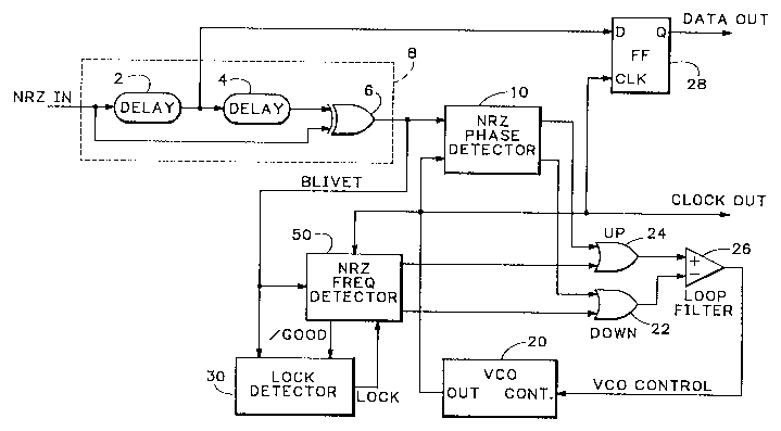
~IG. ~ is a block diagram of the ~R7 clock an~
data recovery system according to the present
invention;
FTG. - is a schematic diagram of the NRZ
fre~uency detec.or according to the present
invention;
FTG. 6 is a timins diasram il'ustratins the
operation of the ~3RZ frequency detector acc^rding
tc the present invention; and
FIG. ? is G bloc!~ diagram of the lock detector
accordins t- .he present invention.

lS Detailed Description
FTG. 3 is a bloc'.~ diasram o~ a portion of the
NRZ clock and data recovery circuit accordins to
the present invention, with an inset schematic
detail of the phase detection circ~itry 10. This
desisn lends itself to in'esration anc provides
automatic centering of the clock edge within the
bit interval in a manner that is independent of
analog delays and process and tem?era.ure
variations.
The ~3RZ data input i_ apolied tc a uni~ue
"blivet" senerator 8. ~ "blivet" is a pulse indi-
cative of a transition, either low-goins or hish-
going, in the ~3RZ data. Internal to the blivet
qenerator 8, the NRZ data input is applied to one
side of exclusive-OR ~OR) sate 6 and also to two
matching delay elements ~ an~ 4 in series, a~ter
which the doubly delayed output of those ~elay
elements is applied to the other side oE the XOR
gate 5. In addition ~ generatins blivets, blivet
generator 8 also provides an NRZ output that is


delayed by one half of the blivet width.
mhe blivet output of the blivet seneratcr is a
pulse whose duration is he sum of the delay
im2osed by the two matching delay elements ~ and ~.
As will be further explained below, the sum of
thcse delays should be less than one half of the
bit interval of the ex?ected data, but as long as
possible within that cons~raint.
~he blivet output of the blivet generator 8,
from XOF~ sate 6, is a~lied to NRZ phase detector
0, which also receives a cloc'~ ou.put from a VCO
~0. mhe NRZ phase detector l~ comQrises AN~ gates
12 and 14 and inverter 16. The NRZ phase detector
10 generates two sisnals, an "up" sisnal that goes
to the "+" input of loop filter ~6, and a "down"
signal that goeC tc ~he "-" input of the loop
filter 26. The "up" and "down" signals are used by
the loop filter 2fi to prcduce the control voltage
for VCO 20. The loop filter ~, which is suitably
a charge pum2, receives the "up" and "down" pulses
from the NRZ phase detector 10 and integrates their
difference into an analos VCO control signal with
only low frequency components.
As will be further exptained ~elow, thc effec-
tiveness of this invention relies on the centering
of the low-going edge of the ~CO C recovere~ clock
output within this blivet.
If the VCC output low-going edgc is already
centered within the blivet ?roduced by the XOR
gate 6, the duration of the out?u. from ~ND gate l
is the same as the duration of the output from A~ID
gate 14, and the inputs to the loop filtee ~6
cancel, indicating that no fre~uencv ad~ustment is
necessary and the loop filter ~6 ccntinue_ ~o
produce an unchansed ~'CO con rol signal.


I~- the ~cwnward trarsition of the ~CC ~0 clock
signal output is late within the blivet, the output
o ~il5 sate 1- has a longer d~ration than the
output of A~ gate 14, and the "up" input to the
1GOP filter prevails over the "dcwn" input and the
VC0 control voltase out?ut of the loop filter ~6
increases the ~IC0 frequency to cause the next low-
going edse to occur sooner wi~hir. the blivet
interval.
Conversely, if the ~ownward transition of the
VC0 0 cloc~ si~nal is early within the blivet, the
output of ~.ND sate 1~ has a longer duration than
the cutput of AMD gate 12, and the "down" input to
the 'oop filter ~6 prevails over the "up" input and
lS the ~.'C0 control voltage output of the low?ass
filter 6 decreases the VC0 fre~uency to cause the
next low-going edge to arrive later in the blivet
interval.
It will there'ore be seen that regardless of
the pc,sition of the cloc~ signal relative to the
center of the blivet, the ~IRZ phase de'ector 1~ and
loop filter 26 operate over time to for^e the
downward edge o~ the cloc~ signal ~rom ~C0 30 tc
the center of the blivet interval.
Because the delay elements ' and a are
identical, they produce equal delays des?ite
process and temperature variations. ~herefore,
changes in process or temperature af~ect the blivet
wid~h, which affects ~he ~I~Z ?hase detec~or's
sensitivity, but not its ability ~o properly detect
phase differences. Sensitivity increases with
increasing blivet width, because the dif'erence
between the widths of the "up" an~ "down" "ulses
can be greater.
~he c1oc'~ output ~,f the ~'C^ ~ is a'so a~?? ied

r~


to ~h~ cloc~ i~put of 'li2-flo? ~. mh~ D i~pu' o'
'lir-flop 2~ is connec~ed tc reseive the once
de~a~fe~ ~r~z data output cf the bli~et cenera,cr ~3,
from the out?ut of delay ele~ent 2. In .he
approach u'ilized in ~his invention, the abili'y to
?osition the clock edse 'hat cloc~s the dat2 into
flip-flop 28 in the center of the "eye" of the bit
interval depe~ds on the centeri.,s of the opoosite
clcck edge within the blivet, as described a~ove.
The VCO is balanced to have a near perfect 50%
duty cycle. So, with the ~CC 2C clock output low-
soins transitions centered in the blivets from XOR
gate ~, the high going tr2nsition.s are glaranteed
to occur uhile the data ?resent at the junction of
the two delay elements 2 and 4 is rish' in the
middle of the bit interval. This is because the
falling clock edge occurred half of blivet after
the end of the las. bi' interval, and data at this
junction is also de~ayed by one half blivet at the
time of the rising clock edge. The D inpu. of
flip-flop ~8 is conr.ec~ed to this junction between
the delay elements ~ and ~ and is cloc'~ed by the
rising ed~e of the VCO 20 output cloc'~ sigr,als.
mhus, the circuit shown in FIG. 3 reliably recovers
NRZ clock and data signals an~ lends i~sel' tc
integration into an TC.
mhe circuit shown in FTG. ' only performs
phase detection, not frequency detection. Vet
frequency detection permits much more efficient
frequency acquisition by ~ ph2se lock loo?. ~onse-
quently, referring now tc FTG. ~, a complete system
for NRZ clock and data recovery includes 211 of the
circuitry shown in FTG. ', plus an ~PZ frequency
detec'or 50, a loc~ detec'or 30 ar.~ 0~ ga'es ^4 an~
22 for combining the "U?" ~nd "dcwn" out?uts of the

r~


phace and NP~Z frequency detectcrs hefore they are
presented to the locp filter 6.
In the fu!l system shown in F~G. 4, the blivet
signal is supplie~ to the NRZ frequency detector SQ
an~ the lock detector 3Q, as well as the NRZ phase
detector 10. The NRZ frequency detector 50 also
receives the clock output of the VCO 2C an~ a
"lock" signal from the loc~ detec.or 30. Li~e the
NRZ phase detector 1?, the ~IP~Z frequency detectcr
50 produces "up" and "down" signals to steer the
VCO 20 via the loop filter 26. These "up" and
"down" signals are combined with the "up" and
"down" signals from the ?IRZ phase dete-tor 10 by up
OR gate 24 and down OR gate 22. mhe ~IRZ frequency
detectcr 5Q also produces "not-good" sisnals that
inform the lock detector 30 when the present blivet
is soing to cause an "up" or "down" sisnal.
Referring now to ~IG. ', the W~Z frequency
detector 50 contains four flip-flops 52, 57, 58
and 59 that are clocked by the risins edge of the
blivet signal and one flip-f10p 53 that is clocked
by the falling edge of the blivet signal, due to
the operation of inverter 51. Flip-f1OpS 5~ and 53
monitor the clock output of the VCO 2~ on opposite
edges of the blivet signal. A "good" blivet is a
blivet whose rising edge occurs while the ~CO O
cloc~ out is hish and whose falling edge occurs
while it is low. A good blivet therefore sets
fli~-flop 52 an~ resets flip-f10F 53. NA~ sate 54
monitors the Q output of f lip-Çlop 52 and the /Q
output of flip-Flop 5~, anc pro~uces a low output
whenever a good blivet has been detected by these
two flip-flops.
The Following table summari~es the information
inferred by the NRZ frequency detector 5~ circuitry


from the relationship be.ween the clock output
level and the blivet edges:

CLCCK/BLIVET IMFE~ENCES
High-going Low-ccing Fre-uency
Edae (F~5~) Edge ~FF5~ Inference
1 ~ good
1 1 Too Low
0 0 Too High
1 Unclear (?)

NAMr sate 55 mcnitors the states of fli?-flops
52 and 53 for the "too-low" condition, i.e., both
flip-flops having a high ou'pu.. The ~hird input
to this NAND gate 55 is fro~ the D-C fiip-flop
created by r1AND sates 62 an~ 63, which produccs a
high out?ut from NAND ~ate 62 and a low output from
NAND gate 63 when the f equency is toc high. ~he
reason for this thied input to NAr~D sate 55 is to
prevent going directly from a "too-high" ccnditio~.
to a "too-low" condition without soing through a
good state in-between. Thus, when the last state
out of the ~RZ frequency detec.or was "Down ~too-
high)", NAND gate 55 is prevented from producing an
active-low output indicating that the next state
should be "Up (toc-low)" by the low out?ut of NAND
gate 63.
Similarly, NAr!~ gate 56 monit^rs the states of
flip-flops 5~ and 53 for the "too-high" condition,
i.e., bo'h flip-flcps having a low outpu,. An~, i
the same way as before, a high output of ~AND
gate 61 in the other D-C flip-flcp, in~.icating that
the last state was not "'oo-low", is reqltired
befoee an active "~co-hish" sicnzl can bc produced.
~he C-C f'ip-flops 6~ and 6~, co~p~ising ~!AND


gates 60,61 and 5~,63, hold the last '~no~n
frec~enc~ direc~ion, ~Go-low, ~oc-hi~,h ^r neither,
until a ~sood blivet oc-urs. An active low ~good
sisnal a'tempts tc clear bcth of the D-C flip-
flo?s, and will do so in the absence of an active
low ,~tco-low or ~too-hi~h sisn21.
The states of the ~t~.?~D sates 54, 55 and 56 are
cloc~ed intc flip-flo?s 5 " 5~ and ~9, respec-
tively, by the rising edse of the next blivet, if
the signal lock is inactive low, indic tins that
the ?hase lock 1oo? is not loc~ed. If the sisnal
lock is active high, indicatin~ that a r,hase lock
loop loc~ has beer. detected, the signal lock ~orces
the /good flip-flop 57 to its cleared state,
producins an inactive hish output from that flip-
flip, which indicates that the state is "good'.
The active high lock signal also forces the "too-
70W" an~ "too-hish" flip-flops tc isncre their
inputs from NA~D sates 55 and 56, respectively, and
produce inactive hish outputs. Thus, uhile the
loop is locked, the NRZ frequency detector cannot
produce any out?ut to disrupt that lock, leavins
control entirely up to the ~RZ phase detector 10.
Note, however, that even while the loop is
locked and the up and down outputs of the ~RZ
frequency detector 50 are disabled, it can still
produce /sood (blivet) signal outputs from NAND
gate 5~. Thus, as will be further explained below,
if enough ~good blivets are detected, the lock
detector 3~ can respon~ by decre~entins down ~o
below its one half full level and soing ~o an
unlocked condition.
Referrins now to FTG. ~, a series o' blivets
prc~uces appro?riate results in the p.ese~ce of
3S three differen~ cloc~. ~requencies, one correc~, one

t


too-hish and onc too-low. In FIG. 6, socd rela-
ticnships ~etween blive~s an~ clcck levels are
indicated by "O"s abcve clock sisnal, while too low
re7ationshi?s are indica.ed with ar. "L" and too-
highs ~ith an "II". Unc7ear resu'ts, where the
clock is low fcr the risins blivet edse and high
for fallin~ blivet ed~e, are indicated ~ith a "?".
Everythin~ is simple for the "Corrcct Clock
Freq" line, with each hlivet producins a "O". The
"Clock Low" line is much more interesting,
producing the sequence of relationshipc:
"OCL~??'IOC?'-. The unclear, ?, indications are
totally unrecognized by the circuitry shown in
FIG. 5, so the "H" at blivet 7 is ignored because
the last indication was a ~lr " and so the output of
NA~7D aate 61 is low disa~ling MAMD gate 56 which
would otherwise detect this "H". Even though the
"H" is not detected, the .ailure tc satisfy ~A~D
gate 54 because the Q out?ut of flip-flop 52 is low
causes the output of MAND sate 54 tc co high, and
:~ this hi~h is clocked into flip-f7o? 5' by the next
blivet (blivet 8~. The continui~g hish output cf
flip-flop 57 has no effect on the D-C f'ip-flops
comprising NAND gates 60,61 and 6~,6'.
The sood blivet at blivet ~ is detectcd by
NA~D sate 54, whose output goes low in response.
The sood state of flip-10ps 52 and 53 also means
that neither of the other MAMD gates 55 or 56 are
satisfied. The low out?ut of M~ND gate 54 is
clccked into flip-flop 5' on the rising edae of
blivet 9. The same rising clock edge of blivet 9
also cloc!~s the high levels that are present on the
output of MA;~D qates 55 and 56 into flip-flo?s '3
and 59, respective~y. The low out?ut of ~'ip-flQp
57 immediately clears the two D-C flip-flo~s 6~,61

r! ~


and 6~ , so that their outputs on N~!D gates 6C
and 62 become lo~, since both of both of their
inputs are now high. ~hQ cleare~ states of the D-C
lip-flops 60,61 and 62,63 enable the third inputs
tc ~A~D gateC '5 and 56, allo-~ing them tc detect
the next high or low s~ate. lf the frequency were
now correct, ~ostly gocd blivets would be detected
from now on and the N~Z frecuency detector wouLd
behave as it does on the line labelQd "Correct
Cloc~ Freq".
In the absence of ,itter, an incorrect
frequency will produce indications like those shown
in F G. 6, in which the desired indica.ion always
follows a good blivet, and any erroneous indica-
tions always follow a desired indication anC are
locke~ out by it. In the presence of jitter,
however, erroneous indications sometimes follow a
good blivet and reach the out2ut. Even in the
presence of heavy jitter, though, the desired indi-
cations always heavily out-weish the erroneous ones
and the system successfully locks onto the correct
frequency.
For the NRZ frequency detector ~0 to work
correctly, the blivet length has to be less than
one half of the bit interval. And, since resistGrs
implemented in silicon and metal capacitors both
have tolerances of up to +/- 2Q~, and the delay
elements 2 and 4 are based on an RC product of such
devices, the worst case delay tolerance could be as
bad as +/- 40~. Thus, if the delay lines are
designed to produce a ccmbined delay of 35~ of the
bit interval, the worst case deviation still leaves
the resulting tota' delay un~er half of the bit
interval, thereby permittins the N~ fre~uency
detector ~ to function properly.


ReCerrins now tc F_G. ', the lock detectcr ~C
receives as its inputs the blivet sisnal and the
~goo~ signal. Counter 1~ is a saturating up/down
counter. A saturatins counter is a counter that
does not wrap aroun~; when it reaches a ful1 coun',
it s.ays there as additional in~re~ent sisnals are
received. The saturatins up~dcwn ccunt_r 42 is
incremented b~ incrementing means 38 whene~er a
"sood" blivet is detecte~ by ~ sate ' , and
decremented by ~ecrementing means 40 whenever a
"bac" blivet is detected by A~D sate 36. lnver'er
34 chanses the /sood signal into a sood signal for
~ND sate 32. When the count in the counter reaches
a threshold, for instance, more than half full, a
"lock" sisnal is generate~.
The ratio of the increment step size
(typically one) tc the ecrement step size
(typicall~ some multiple of increment size) deter-
mines the tolerance of the lock detector 30 to
jitter. A 1:4 ratio has been found to provide a
suita~le jitter tolerance. The size of the
saturating u~down counter 42 (in bits) determines
the integration time of the lock detec~or ~0, ~nd
hence its response time to a locked oz unlocked
concition. ~here is a trade-ofc between the speed
with which a lock is identified and the certainty
of that identiCication. Tn the present applica-
tion, 12 bits of binary, for a total count of 40a6,
has been found to be a suitable length for this
counter, so that a lock indication appears after a
count of 2048. If jitter is minimal, a loc~ is
achie~ed in a~out l~ microseconds at ~?0 Megabits
per second.
ThiC lock detectcr 30 implemertation is
completely digital and therefore does not require


an an31Os integ!ation capacitcr an~ associate~ IC
?in. This is a significant benefit in some appli-
caticns where 2 shortage of IC pin- is an important
~esisn constraint.
~h~s, i. can be seen that the present inven-
tion provides an improved ~RZ clock and data
recover~ syctem that len~s itself to in~ecra~icn,
that includes a NRZ phase ~etector, an `i~Z
frequency de'ector anc a lcck detec'cr, and that
provides au~omatic centering of the clock edge
withiq the bit interval in a manner tha~ is
inde?endent of analog delays and process and
temperat~re variations.
While a preferred embodiment cf the present
invention has been shown and described, it will be
a?~arent to those skilled in the art that many
changes and modifications may be made without
departing frcm the invention in its broader
aspects. The claims that follow are therefore
intended to cover all such changes and modifica-
tions as fall within the true s?irit and scope of
the invention.


Representative Drawing
A single figure which represents the drawing illustrating the invention.
Administrative Status

For a clearer understanding of the status of the application/patent presented on this page, the site Disclaimer , as well as the definitions for Patent , Administrative Status , Maintenance Fee  and Payment History  should be consulted.

Administrative Status

Title Date
Forecasted Issue Date Unavailable
(22) Filed 1992-02-26
(41) Open to Public Inspection 1992-09-08
Examination Requested 1992-10-28
Dead Application 1996-08-26

Abandonment History

There is no abandonment history.

Payment History

Fee Type Anniversary Year Due Date Amount Paid Paid Date
Application Fee $0.00 1992-02-26
Registration of a document - section 124 $0.00 1992-10-25
Maintenance Fee - Application - New Act 2 1994-02-28 $100.00 1994-02-03
Maintenance Fee - Application - New Act 3 1995-02-27 $100.00 1995-02-24
Owners on Record

Note: Records showing the ownership history in alphabetical order.

Current Owners on Record
HERSHBERGER, DAVID L.
GRASS VALLEY GROUP, INC. (THE)
Past Owners on Record
None
Past Owners that do not appear in the "Owners on Record" listing will appear in other documentation within the application.
Documents

To view selected files, please enter reCAPTCHA code :


To view images, click a link in the Document Description column. To download the documents, select one or more checkboxes in the first column and then click the "Download Selected in PDF format (Zip Archive)" or the "Download Selected as Single PDF" button.

List of published and non-published patent-specific documents on the CPD .

If you have any difficulty accessing content, you can call the Client Service Centre at 1-866-997-1936 or send them an e-mail at CIPO Client Service Centre.


Document
Description 
Date
(yyyy-mm-dd) 
Number of pages   Size of Image (KB) 
Representative Drawing 1999-07-08 1 16
Drawings 1992-09-08 6 93
Claims 1992-09-08 14 388
Abstract 1992-09-08 1 35
Cover Page 1992-09-08 1 13
Description 1992-09-08 14 481
Prosecution Correspondence 1993-02-02 1 24
Examiner Requisition 1995-11-17 3 120
Office Letter 1996-07-26 1 23
Office Letter 1992-12-03 1 40
Prosecution Correspondence 1992-10-28 1 53
Fees 1995-02-24 1 61
Fees 1994-02-07 1 57