Note: Descriptions are shown in the official language in which they were submitted.
- - 2062413
- 1 -
MOLDED OPTICAL "ACKAGING ARRANGEMENT
Back~round of the Invent~on
Technical Field
The present invention relates to optical p^^~n~ technology and, more
5 particularly, to a molded optical ~ ~ing arr~ngtom~nt
Description of the Prior Art
There exist many dirrvlcl~- arr~nge .~ r~l~ for p; ck~ing optical
co.~ ic~tion a~ng ,~nt~ For eYi~n ple, the optical device (e.g., laser, LED or
photodiode) may be ~tti ched to a mount which is subse:~luentl~ aligned with and10 ;~tt~hed to a base ...~ .bel, the base ,lænlbcr including lensing ele~ s to facilitate
coupling of an optical fiber to the optical device. In most cases, the base ,~mlx,
will include a spherical lensing cle.,lent to maximize the optical coupling. Thearr~n~em~nt of the mounted optical device, base n~.mhe~.r and lens is often l~re.lcd to
in the art as an optical sub~-sembly, or OSA. The electronics required for ope.atillg
15 the optical device (a driver circuit for a tr~nsmitt~r, or an amplification and deci~ion
circuit for a Icceh,~,r, for example) may then be se pd~t~ ly assembled (on a printed
wiring board, for example) and connec~ to the optical ~Ub~C~ ..hly by
con~,el,~ional el~ctric~l leads. ~lt~tively, the elc~ ~ics may be fully enclose~ in
a separate housing, with only the leads exposed for conn~tion to the optical
20 sub3~vembly. An advantage of using separate housings for the electronics and optics
relates to the ability to interchange the cG,l,ponenls as required for dirrelci~t
applications. For example, a data link application may operate with TTL electronic
signals, and another application (with the same optics) may utilize EC~ CleCll~.liC
signals. ~ddition~lly~ if either the electrical or optical po~hon of an arr~n~ment
25 were to eA~Iience a failure, the working portion could he discol n~d and re-used
with another &~ f nt A major disadvantage of sepaldt~ p~o~ging is the
overall siæ of the resultant arr~n~ement. With two se~,~ p~c~ges, or an optical
p~el~ge Illounted on a printed wiring board, the arrangement Iequires a rather large
space. Further, such an aIrangement is susceptible to electrical noise introduced by
30 the n~ss,..;ly long lead lengths between the electronics and the optical device. The
elect~ic~l noise factor becomes a ~i nifin~nt concelll at bit rates e~ in~
a~ploAill~dlcly 10Mb/s. Also, long leads may limit the ma~llulll bit rate of either a
...;lt,~, or receiver, due to parasitic lead inductance (limits tr~n~mitter) or
parasitic cara~it~nces (limits receiver).
20624 1 3
-2 -
These and other concerns have led to the development of package
designs which provide for the electronics and optical device to be housed in thesame unit. Many of these unitary packages are relatively expensive, as a result of
using a hybrid integrated circuit (HIC) arrangement for the electronics, with anoptical subassembly attached to the HIC. Additionally, the piece parts used in the
optical subassemblies associated with these packages are often formed of machined
metallic components, adding to the cost of the system. Further, these optical
subassemblies have been known to experience alignment difficulties. Fabrication
problems may also exist with respect to mating the various piece parts (i.e., outer
housing, optical subassembly and HIC). Lastly, in many instances, the packaging
processes for a transmitter and receiver are often very distinct, leading to
manufacturing problems and increasing the overall expense of the packaged system.
An improved package designed is disclosed in U.S. Patent 4,911,519
issued to W.H. Burton et al. on March 27, 1990. In the disclosed arrangement, the
HIC of a conventional package is replaced by a conventional 16-pin dual-in-line
package (DIP) which includes a specialized pair of end prong leads for attachment to
the optical subassembly. The DIP and optical subassembly are subsequently
assembled within a plastic molded package frame. The plastic molded frame is
configured to include a molded optical connector receptacle for subsequent
attachment of a connectorized optical fiber. The arrangement is subsequently
covered with a metallic lid which is grounded to the package floor. A significant
savings is realized by the utilization of the DIP, as well as utilizing a molded plastic
piece part for the frame/connector assembly.
Although the Burton et al. arrangement is considered to be a
significant advance over the prior art, the need remains to further simplify optical
packaging techniques, with respect to limiting the number of separate assembly
operations, in light of rapidly growing markets which will require many thousands of
such devices in as a cost competitive arrangement as possible.
Summary of the Invention
The need rem~ining in the prior art is addressed by the present
invention which relates to optical packaging and, more particularly to a molded
optical packaging arrangement.
20624 1 3
-
-2a-
In accordance with one aspect of the invention there is provided an
optical communication arrangement comprising: an active semiconductor optical
device; electronic circuitry, required for the operation of said active semiconductor
optical device; CHARACTERIZED IN THAT the arrangement further comprises a
leadframe section attached to the electronic circuitry; first molded packaging
disposed to encapsulate said electronic circuity and a first portion of said leadframe
and further comprising a support member molded to and encapsulating a second
portion of said leadframe; an optical base member for supporting said active
semiconductor optical device and disposed to rest upon the molded support member;
and second molded packaging disposed to cover both the encapsulated electronic
circuitry and the optical base member.
In accordance with another aspect of the invention there is provided
an optical communication arrangement for use with a pair of active optical devices,
the arrangement comprising: a leadframe section; first electronic circuitry, required
for the operation of a first optical device, attached to said leadframe section; second
electronic circuitry, required for the operation of a second optical device, attached to
said leadframe section in a location physically separate from said first electronic
circuitry; first molded packaging for encapsulating said first electronic circuitry and
a first portion of said leadframe and including a first support member molded to and
encapsulating a second portion of said leadframe; second molded packaging for
encapsulating said second electronic circuitry and including a second molded support
member; first optical means, including an active semiconductor optical device,
coupled to said first encapsulated electronic circuitry and including a first base
member disposed to rest upon the first molded support member; second optical
means, including an active semiconductor optical device, coupled to said second
encapsulated electronic circuitry and including a second base member disposed torest upon the second molded support member; and third molded packaging disposed
to cover the first and second molded packaging and the first and second optical
means.
3 o In an exemplary embodiment of the present invention, a leadframe
section is utilized for the placement and attachment of electrical circuitry required to
operate the associated optical device (e.g., a driver circuit for a transmitter and/or an
amplifier and decision circuit for a receiver). A first molding
.,
2062~13
- 3 -
operation is then pe.r."-,~d tO encapsulate the electronics. A support ..~...~1 is also
molded during this step, where the support ~ I.~r is uscd for the later plnce~nt of
the base l~ llber of an optical s-lbscse...bly. Subs~uent to the first rn~l~ing
o~l~tion, an optical device and asso~ i5~'.d base nl~ ".bel are positiQned with and
5 attached to the e~ Jl^-ed elec~nics. The co.llbil~dtion of the electronics andoptics is then e~ 1 ted during a second nl~ing operation to foml the final
p~r~g~ q~ngen~nt
In an ~l~n~q~ive c~ of the present invention, im~u~ed EMI
~hi~1~1ing may be provided by utili~ing a n~t~llic plate which is disposed over and
10 electrically coupled to the c-~ral,s llqt.~ electronics. The shield plate is ~tt~h~ tO
the ~n~n~nt prior to the final en~al ~ul~tir~n step.
An e~enlplqry alT~ngen~nt of the present invention may utiliæ an
optical device (and lensing clell~er.t(s), if ~ui,~,d) inse~d within a con~
optical subassembly (OSA), where the elec~Tical leads exiting the optical device are
15 connected to the leadframe and the base ~ be~ portion of the OSA rests upon the
molded support ...f ~ ,.. The base 1l~ , which houses a lensing cle.l~nt (for
example, a spherical lens, fiber stub, or any other arrn~ Pnt suitable for providing
optical coupling), may be formed to include a ,~c~pt~cle po~tion required for ~ephysical ~tt~rhm~nt of a conn~lo- ;7ecl fiber to the pa~ gç Alternatively, the final
20 ml~ing for enr~rsul~ting the optics and cle.,llonics may be design~ to provide the
conl-e.-lor rece~lacle as a part of the final molded outer p~cl~ge
In an alternative arrangement, the optical device (for example, a lensed
LED) may be physically attached to the Ic~l~ c. In particular, the leadframe maybe c~nfigllred to comprise a paddle-like lead for ~ thereto of a first majcr
25 surface of the optical device. The paddle includes an a~~ e aligned with the active
region of the optical device so as to allow for the passage of the optical signal
through the leadframe. A second lead is used to provide the lc~ ining el~;llicalJ hllh nl to the opposing majcr surface of the optical device. For this
i~rT~ng~m~nt, a base llf Ill~r~ positionçd in the support ..lf ...be" includes a lensing
30 element to f~iliti~te coupling of the optical signal between the optical device and an
ntt~h~.d fiber. The base n~lllber may be configured to include a com e~lor
~ p~cle. Altem~tively, the final outer pac~i~ may be molded to include the
required recept~cle.
4 2062413
Brief Dcscription of the Drawin~
Referring now to the drawings, where like numerals lepl~senl like parts
in several views:
FIG. 1 illu~lldt~,s an exemplary leadframe alT~n~n~nt suilàble for use
5 in ~ooci~tiQn with the teachings of the present invention;
FIG. 2 i~ str~tes a portion of the lead~ame of FIG. 1 illu~llali~i~g the
all l.."f n~ thereto of the el~iu,~ics ~si~t~ with a particular e ~ of the
present invention;
FIG. 3 illu~ dtes the arrangement of FIG. 2 subsequent to the f~rst
10 encapsulation, including the formation of the support member,
FIG. 4 illu~ tes the a~ngen-ent of FIG. 3 subsequent to the
~tt~ ment thereto of an optical subassembly;
E;IG. S illus~ iates the arrangement of FIG. 4 subsc~uent to the final
c n~al.su1~tion, where the conn~lo~ receptacle is molded as part of the final outer
lS package;
FIG. 6 illu~ t~s an al~,Qa~ e arT~ngenlent of the present invention
subsequenl to the first e n~ tion step;
FIG. 7 illu~ t~,s the a~ngelT~nt of FIG. 6 subsequent to the
att:~hn~,nt thereto of an optical device and associated base ..~ ...hf ., the base
20 ~ ber configured to include a conneclor rec~pt~le;
FIG. 8 illu~ t~,s the arrangement of FIG. 7 subs~uenl to the finzl
molding, where the lecept~cle portion of the baæ ~lle~l~, remains expoæd beyond
the outer p~age housing;
FIG. 9 illu~h~t~s an ~ltem~tive embo~iment of the present invention,
25 prior to the final encapsul~tion~ particularly suited for the con.bined p~lra~in~ of a
pair of optical devices such as in the formation of a molded ll~nsce;~e. p:lc~a~,
where in this embo~litr~nt the optical sub~csæ- .-blies are formed to include a pair of
Conneclor receptacles; and
FIG. 10 illu~lldtes an enca~s.llated view of the arran~..Yn~ of FIG. 9,
30 particularly illustrating an altem~tive connr,~lot l~,cel)ldcle design.
Detailed Descripffon
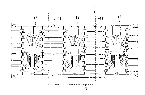
Referring to FIG. 1, an exemplary leadframe 10 is ill-lst~t~d which
incllldes a large l~ull.~r of severable leadframe sectiQn~ for use with a r~ul~ber of
separate Optl~ ele~ unic packdges. It is an advantage of the present invendon that
35 the use of a leadframe structure allows for the siml~ neolls f~bric~ion of a large
number of opto-el~;llonic packages, such as tr~n~ and/or
- 2062413
- 5 -
transceivers. Similar to convention~1 ele,c~ ic integrated circuit processing, aplurality of integrated circuits may be siml-lt~nPously attached and wirebonded along
locations 12 of leadframe lO. In accol~ance with the teachings of the present
in~ , the plurality of integrated circuits are ~im~1n~ U$ly e-n~p~u1~
S lea~ing t,-l~osed the leads required fc~r cubs-pquent ~ ",~.,t~ thereto. In particular,
an ~ ~ plurality of optical arran~C ~ are s.lbsc~ ..tly attached to the
Illo!d e ~ cle~ nics and the combination of electronics and optics er ca~ ted tofo~med the final ~ gP asselnbl~ . When the final mol-lin~ operation is cs~...ylet~
leadframe lO may be severed along dotted lines 14 to form a plurality of final
10 p~ ge ass~-nblies. The ~."Aining figures i~ str~te a single le~lrl~ section and
the various items ~oci~t~ thc..,.. illl. It is to be understood that the illustration of a
single leadframe section is only for the sake of ~ cu~sion and in general a larger
nu~l~. of opto elec~nic ~sPmb1iPs are sim1~1t~nPously fo~med in p~uc~;o~-
A single leadframe section 20 is particularly illustrated in FIG. 2.
15 Section 20 includes a central ground plane paddle 22 to which an intc~ a~ circuit24 is attached. Integrated circuit 24 is subsequently co~lplul, using wi~bol~ds for
e~, ..p1e, t~ sP1ec~ leads 26 of leadframe secdon 20. A sep~dt~ c~a~ e elc~..
28, which may be required for certain IlA.I~ l and/or receiver confi~rations~ ischlo~l to lca~lln~ll~ secdon 20 as shown in FIG. 2. Subse~uent to the attach~ent20 of electronics 24,28, a molding operation is pc.~ ed to en~ te the elect~onics
in a first housing 30, as illu~l. ated in FIG. 3. In this part.cular embol1impnt~ used for
the ~tt~hmPnt of an optical subassembly to housing 30, a pair of end prong leads32,34 of lca~lLall~ section 20 remain exposed. End prong leads 32,34 may be bentu~.~s at an angle of, for e~am~lc, 90 (as shown) to facilitate the later att~hment
25 of a pair of OSA leads. Alternatively, end prong leads 32,34 may remain in the
plane of leadframe section 20 and the OSA leads bent do. I~wal~l to co,.~plet~ the
k...rnt As shown in E;IG. 3, the first mol lin~ ope.alion is also used to form asupport ~Ill~r 36, where as discu~ above, the base portion of an OSA is
positioned to rest upon support ~f ..l~r 36. Support l.~ nber 36 has been found to
30 illlpl~.e the stability of the assembly during the subsequent moldin~ operation.
Referring to FIG. 4, an optical subassembly 40 is illu~ t~d as ~tt~ched
to the aIrn~n~nt of FIG. 3, with base l~.e ..~l 42 of optical ~ub~se ..bly 40
po~ition~ to rest upon support ~ ber 36. An optical device 44 is ~up~d on a
mount 46 such that electrical leads 48 of mount 46 may be coupled to end prong
leads 32,34(FIG.3). Base l.~ 42 may be attached to support Ill4nl1~r36 using
an adl~h,~" such as an epoxy, or merely held in place with a mandrel. The ~.ah~l
- _ 20~2413
- 6-
is utiliæd to pl~ellt motion of OSA 40 and block the entry of any molding m~ten~l
into base llf,~b~ 42 during the final mol~ing operation. FIG. 5 illu~ ~s a finalp~c~ of the arr~n~em~nt of FIG. 4. As shown, OSA 40 and enf ar~ul~t~
cl~llollic hous;ng 30 are colll~l~tPly covered with a molded outer holl~;ng 52. For
S the particular c~hodh~n( of FIG. 5, base ~ ,r 42 (par~ally shown in ph~.-tnm)
is completely emhe~ded within ho--cin~ 52 and hous;n~ 52 is formed to include a
con~ t~r l~,c~U~le 54 aligned with base "~....k,,r 42.
As mentioned above, an e~.c.~l~l molding ~hni~ e which may be
used to form both electronic inner p~ck~gç 30 and the final outer p~a~ 52 is
10 l~ansr" ~TU~ ling, as used in conventional inte~ted circuit p~ ing In ~la.lsr~r
m~lding, a plchr~l~A charge of tl~"l,oset m~lding CU~PO~J~ is moved from a
dielecll;c pl~heat~- into the mold cavity through a single inlet port. Transfer
m~'1ing, as is well-known, is best suited for the type of insert mnl~ling where it is
desired to precisely form certain Ç~ s, such as the conn~lc). receptacle of this15 par~icular c ll~bodill-cnl of the present invention. During the molding process,
leadframe 20 of FIG. 2 (i.e., leads 26) is clqmped in place to hold the co...po~lenl~ as
st~qti~nq y as possible. A first, l~la~i~ely simple, rectangular mold is then used to
en~p~ ~lst~ the el~llonics. For the second n~k1ing operation, leadframe 20 is again
clqmred into place and, as mention~ above, a mandrel may be used to both pl~,~en20 motion of OSA 40 and create inner bore 53 of receptacle 54. For the second
operation, a mold inclllding the design of connectQr recep~cle 54 is used to
encapsulate both the housed electronics . nd the optical COInpOl e.lls.
In an alt~",-ali-e embodim~nt of the present invention, the use of a
separate optical subscsemhly may be replaced by the direct attacl~nt of an optical
25 device to the leadframe s5~ ;a~ A with the cl~l,onics. ~;IG. 6 illL.i.~l~tes an
eYemr1~q--y encapsulated el~~ ic subassclllbly 60 including a spe~isli7~d pair of
leads 62,64 for the direct attachment thereto of an optical device. As shown, lead 62
is formed to coll-~lise a paddle-like shape and may include an apel IU1C 66. An
optical device 68 (shown in ph~nlf,...) is ~stt~ ~hed along a first major surface to
30 paddle 62 such that the active region of device 68 is aligned with aye~ e 66.Alte".ati-ely, device 68 may be att~rll~A. to the opposite side of paddle 62 such that
an ape~ is not required. The l~.n~inil~g electrical contact to device 68 is formed
by wilcbon-ling the oppo~ing major surface of device 68 to lead 64
As with the a~ngem~nt described above in a~soc~ on with FIGs. 1-5,
35 the arr~ng~ nt of FIG. 6 may require the utili7~tiQn of an optical base ln~ to
f~ilitat~ the optical coupling ~t~.een device 68 and an conn~t~ optical fiber.
7 2~6~13
FIG. 7 illustrates an exemplary embodimont wherein a base m~mber 70 is positi~n
upon a support ~ r 72 and att~ch~ to paddle 62 so as to be in optical ~lignment
with device 68. In general, base member 70 may include a lensing element (e..g,
~yk~ 1 lens or fiber stub) to improve optical coupling. For the particular
S e.~ illustrated in FIG. 7, base ..~- --bt r 70 is formed to include a co--n-~lo~
receptack 74. The use of a base .-~...b~ including a~ipt ~le portion thus
.:..y l;r.- s the final m-~lding operation (i.e., no need to mold a receptacle) and ensures
that the receptacle will be opdcally aligned with the ~S~t~ optical device. FIG.8 illu~ll~s the arr~n~n~nt of FIG. 7 subs~uent to the final mr'ling operation. As
10 shown, the mold used for this process is configured to form an outer housing 80 such
that l~cepl~rle portion 74 of base ~ 70 re~ins exposed.
An advantage of the leadframe-based p~ ging t~chnology of the
present invention is that any number of optical devices (and the associated
en~aps~ ted ele~;l,oi ics) may be embeddod within the same molded outer pac~ge
15 In general, ll~e,erolc;, an array-like package may be formed. In one particular
e~bo~1;n~ nl, a pair of optical devices may be ~iml~ n~4usly ellcap~ulated so as to
fo~m, for example, a dual-~va~elength tran~..;lt"r or receiver (or a sparing
a~ngen~nt) or, ~ltem~tively, a llilns~ei~,l including a light llnn~ ;t~ g devioe(e.g., LED or laser) and a light receiving device (e.g., PIN or avalanche phot~i~e).
20 FIG. 9 illu~ ~s in particular an exemplary tlansce;~er p9^~ ~ 90 for_ed in
accordance ~ith the te~ching~ of the present invention. As shown in this view, a first
OSA 92 (housing a light tr~n~mitting dev*e and any required lensing elements)
in~ludes a base m~mber 94 which rests upon a first support Il~m~l 96. OSA 92 is
also el~llonically coupled to e -r~s~ ted driver ekctronics 98. Base l~h,-~ 94
25 of OSA 92 is formed in this particular configuration to include a con~ or
receptacle 100. Similarly, a second OSA 102 (housing a light receiving device and
any l~uilGd lensing ele~ nt~) ineludes a base ~ ~r 104 which rests upon a
second support .~Y~ 106. OSA 102 is then ek~tric~lly coupled to encapsulated
amplifier-decision circuit el~l,unics 108. In order to reduce the effects of electro
30 ma~e~ir in~lr~l~nce (EMI) on the operation of el~lonics 108, a m~t~llif plate 110
may be disposed over p~ ~ 108 and coupled to the ground plane exiting package
108 to forrn an EMI shield. Plate 110 may comprise a Sepalale piece of metal which
is ~ to the leadframe subsequent to the first mol~ing operation (i.e.,
enC~p~ tiQn of the electronics). Altelll&~i~ely, the leadframe utilized for this35 el.~ ;n~ -l may be formed to include a plate portion which may be bent over the
par~ P.d elecl,onics to form the shield.
2062413
- 8 -
FIG. 10 illustrates an encapsulated view of the arran~.nt of FIG. 9,
where thc outer p~lravp~ 120 is molded to completely cover first OSA 92, first
ele~ unics 98, second OSA 102 and second electronics 108. In this particular
embo~ n~, package 120 includes a colmcclo receptacle 122 of the design as
S shown in FIG. 10. In particular, con~ ol recept~cle 122 co~i~s an opPning 124
of s~lffi~P.nt depth that first and second OSAs 92 and 102 remain e~ d Faf one
w.n~ of this a~ ;e~-lf Ot, the mol-lins operation used to foqm
outer package 120 may sim~ ane4~lsly from conn~clor re~eptacle 122.
Al~.~a~ ly, com~-lur receptacle 122 may comprises a pie~e part sepa~ate from
10 outer p~ age 120 which is subsequently clamped over pa~age 120 to form the
arrang~mP-nt as illustrated in FIG. 10.