Note: Descriptions are shown in the official language in which they were submitted.
WO 90116027 PCf/US90/01642
. I 4
r~Q,''~~ '~ '~~.
INFORMATION PROCESSING SYSTEM EMULATION
APPARATUS AND METHOD
FIELD OF THE INVENTIONS
This invention relates generally to information processing
systems and, in particular, to an information processing
system having an applications processor (AP) and a virtual
input/output (I/o) processor (VIOP), the system being
responsive to the operation of the AP to suspend operation
of the AP when the AP accesses predetermined regions of the
system address space.
BACKGROUND OF THE INVENTION~
For certain applications it is desirable to provide an
information processing system which emulates the
functionality of another information processing system.
Such a system is especially advantageous when it is desired
to execute, with a first type of system, application
software developed for a second type of system.
As can be appreciated, in such systems it is desirable that
the software be executed with little or no change. That is,
if it becomes necessary to rewrite portions of the software
the desirability of executing the software onvthe first type
of system is decreased. ' ~~ ~ --
One impediment to this type of system emulation is that the
~'~'~~'~:PaH,F
Wl'D 90/16027 ~. Jlb r : ~.
P(.'T/US90/01642
software is typically written to interact with a specific
type of I/O device. For example, a serial communications
program is written for a particular type of serial ,
communication integrated circuit located at a specific system
address. One approach to emulation may be to provide the
specific types of I/O devices required by the application
software. However, in many types of systems this is not
desirable or practical in that the system may be primarily
used for significantly different applications.
It has been known to provide in such systems a first
application processor which executes the desired application
software and a second emulation control processor. However,
many of these conventional types of systems utilize a
mechanism whereby an access by the application processor to
a specific I/O device generates an interrupt which in turn
invokes specific and different software routines by the
application processor. Such interrupt driven systems
typically require that portions of the application software
be rewritten and/or that additional application software be
provided in order to properly emulate the I/O devices.
Thus," the portability and.. ease of use of the target
application software is compromised.
i
-SUMMARY OF THE INVENTION . . ..:
The foregoing problems are overcome and other advantages are ''~
realized by an emulation method and apparatus disclosed i
below. In accordance with a method of the invention there is
I~VO 90/1607 PGT/US90/01642
_ ~',.Q~~w: ~~.
w a <
3
disclosed for use in a data processing system having at
least a first and a second data processor a method of
emulating with a second one of the data processors an I/O
device accessed by an application program executed by a
first one of the data processors. The method includes the
steps of (a) detecting a read or a write access cycle made
by the first data processor that is directed to a
predetermined address location associated with the I/O
device, (b) suspending the operation of the first data
processor such 'that the access cycle is not completed and
(c) notifying the second data processor that operation of
the first data processor is suspended. The method further
includes the steps of (d) determining with the second data
processor the identity of the I/O device to be emulated, (e)
emulating the I/0 device by .accepting or providing an
information unit associated with the read or the .write
access cycle, respectively, and (f) resuming the operation
of the first data processor such that the access cycle is
completed.
In accordance with apparatuses of the invention there is
disclosed for.use in.an information processing system, the
system including a system bus having a system address bus
and a system data bus and at least two data processors
coupled to the"aystem,bus, emulation apparatus for enabling
a first one of the data processors tn execute;' in ~~~ w
conjunction with~a second one of the data processors, a
program requiring access to predetermined address locations
WO 90/16027 ~ ' ' ~. ' Pf.T/US90/01642
~~~~~ d r~.~. 4
associated with a specific type of device, typically an I/O
device. The emulation apparatus includes circuitry for
detecting an occurrence of an access cycle by the first data
processor to the predetermined address location, circuitry
for halting the first data processor before completion of
the access cycle and circuitry for notifying the second data
processor that the first data processor is halted. The
emulation apparatus further includes circuitry for
indicating to the second data processor a value of the
predetermined address location being accessed and a type of
access to the predetermined address location. The second
data processor includes circuitry for interpreting the
address value arid type of access, for accessing a
corresponding address location having a same type of
specific device or a corresponding type of device and for
causing the first data processor to be released to complete
the access cycle.
$RTFF DESCRTPTTQ~ OF THE DRAWING
The above set forth and other features of the invention will
be made more apparent in the ensuing.Detailed Description of
the Invention when read in conjunction with the attached
Drawing, wherein: . , .
Fig. 1 , is a detailed block diagram. :of ~ an = information
processing . system having. am AP and a VIOP which is
constructed and operated in accordance with the invention;
CVO 90/16027 PGT/US90/01642
Fig. 2 is a black diagram of the information processing
system;
Fig. 3 is a block diagram which shows the arrangement of
VIOP and AP data buffers and latches; and
Figs. 4a and 4b are timing diagrams that illustrate an AP
write cycle and an AP.read cycle, respectively, the diagrams
showing the intervention by the VIOP.
DETAILED DESCRIPTION OF THE INVENTION
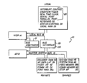
Referring to Figs. 1 and 2 there is shown a block diagram of
an Information Processing System (IPS) 10. IPS 10 includes
an AP 12 , a VIOP 14 , a Master System Bus (MSBus ) I6 and a
VIOP Local Bus 18. The MSBus 16 includes a Master System
Address Bus (MSAB) 16a and a Master System Data Bus (MSDB)
16b. The VIOP Local Bus 18 includes a Local Address Bus
(LAB) 18a and a Local Data Bus (LDB) 18b. A number of I/O
peripheral devices are provided and are grouped into
different categories depending on which:of the buses 16 or
18 that a particular peripheral is coupled to.
In a presently preferred embodiment of the invention the AP
12 is an 80286 microprocessor device.which is manufactured
by the.,Intel Corporation.:of Santa Clare, California. v' This
functionality of_this device is fully described in the~80286
Hardware Reference Manual, published by the Intel
Corporation, the disclosure of which is incorporated herein
wo 9oia6oz2 Pcrius9oio~s4z
~rv ~
6
by reference. The VIOP 14 is a High Performance
Microcontroller (HPC16040) which is manufactured by the
National Semiconductor Corporation of Santa Clare,
California. As such the ensuing description references
specific input/output pins and functions associated with
these devices. It is pointed out however that the practice
of the invention is not limited to only these types of
devices and may be practiced with a number of different
types of microprocessors or other processing devices. The
ensuing description is therefore not intended to be read in
a limiting sense but, instead as a presently preferred
embodiment of the teaching of the invention.
The AP 12 operates over the MSBus 16. A plurality of~5ystem
Peripherals are coupled to the MSBus 16 providing the AP 12
with access to certain of these System Peripherals. The VIOP
14, through bus interface circuitry, also has access to the
System Peripherals. The System Peripherals include a System
Video Peripheral 32' which is comprised of a video
controller, a video memory and a Video I/O. The system
Peripherals also include a System Communication Peripheral
33 comprised of a Communication Controller, a communication
memory and an. I/O ..device. In a presently preferred
embodiment of the invention the Communication Controller is
comprised of a Z-80 microprocessor device having firmware
and other resources to implement a communication port known' ~ -
in the.art as a 928 communications interface. Coupled to the
928 interface may be a VS computer system of the type
WO 90/16027 PCI'/US90/01642
7 ~~~r~a v "~
J~V ~~
manufactured by Wang Laboratories of Lowell, Massachusetts.
As such, and in accordance with one aspect of the invention,
the IPS 10 may function as a VS-type 2256C terminal or may
function as a WANG IBM Compatible (280) Computer. By
example, application software for execution by the AP 12 is
downloaded from a host system via the communication port and
is stored within the RAM 48. In this regard the VIOP 14
totally emulates disk for the AP 12.
The VIOP 14 operates over the associated VIOP Local Bus 18.
A plurality of Local Peripheral Devices (LPDs) 20 are
coupled to this bus, the LPDs 20 being accessed only by the
VIOP 14. The AP 12 has no direct access to the LPDs 20.
The,LPDs 20 include the following devices: an Interrupt
Controller, a Counter/Timer, a Real Time Clock, a Serial
Communication Port and a Parallel Port. Other local
peripherals which are coupled to arid accessed only by the
VIOP 14 include a Keyboard 22, Status/Control Ports 24a and
24b, a l6KByte Local RAM 26 and a VIOP 14 Master Address
Register 28. The Master Address Register 28 is employed by
the VIOP 14 during an access to the MSBus 16 in a manner to
be described. The LPDs 20 and the keyboard 22 are peripheral
devices,of~a type typically found in the processing device v
which is the target ofw the emulation. For example,w an ~~
AT-type data processing device includes'the same peripheral w
devices, but not necessarily the same functionally identical
peripheral devices. As such, any applications software which
WO 90/16027 . , . PGT/US90/01642
;~ ta~.ay 8
-~ ~.. d r
is executed by the AP 12 is written to access these
peripheral devices at predetermined address locations. In
order to emulate the operation of the target processor the
VIOP 14 must detect when application software executed by
the AP 12 has performed a read or a write access to one of
these predetermined locations.
The IPS l0 also includes a plurality of system peripherals
which are located on the MSBus 16. Some of these system
peripherals axe accessed by both the VIOP 14 and the AP 12
while others of these peripherals are accessed only by the
VIOP 14. As such, the system peripherals are referred to as
Private Peripherals and Shared Peripherals. Private
Peripherals are those coupled to the MSBus l6 but which are
accessed only by the VIOP 14. Shared Peripherals are those
peripherals coupled to the MSBus 16 that are accessed by
both the AP 12 and the VIOP 14.
The Private Peripherals include an Address Decoder RAM 30,
Video I/O 42, Communications I/O 34, Data Buffers and
Latches 36 and a Font RAM 38.
The Video, I/O 42 controls the manner in _which data for a
display screen 44 is generated and managed. Iw a presently
preferred embodiment of -the .invention the- Video I/O 42 is
implemented.by a LSI device known as a Paradise PVC4A video - .
Controller which is manufactured by the Western Digital
Corporation. A complete description of the functionality
W~ 90/16027 v PGT/US90/01642
'~ r-.e'..y
e~~.::f.'~~ d a ~.
of the Video I/O 42 is found in the Paradise PVC4A
Specification, published by the Western Digital Corporation.
The Font RAM 38a stores up to two sets of alphanumeric
character fonts. .The fonts are permanently stored in a
System ROM 46 from where they are transferred to the Font
Ram 38a by the VIOP 14 during system initialization.
In regards to system initialization upon the generation of
a reset signal the AP 12 is maintained in a reset condition
while the VIOP 14 is released and begins execution of code
from ROM 46. After performing an initial self-test the VIOP
14 locates further executable code in ROM 46 and transfers
same to local RAM 26 from which the VIOP 14 initializes the
system and eventually accesses a predetermined location to
release the AP 12 from the reset condition.
The above mentioned Shared System Peripherals include a
System RAM 48 and the System ROM 46 which, in addition to
storing the fonts, also stores the system diagnostic and
initialization code. The Shared Peripherals also include a
64K Video Memory 38b and a.Communications buffer memory 40.
In accordance with the invention the Shared Peripherals also
include Stop AP circuitry 50 that generates a'signal to halt'v~r'
the: operation of.: the AP 12 when the AP 12' attempts to access
a predetermined area or areas of the system memory. The
predetermined areas of memory are programmed into the
wo 9oraso~7 ~crrus9oroa6a2
'sra d s
Decoder RAM 30 lay the VIOP 14 during system initialization,
the Decode RAM 30 having address inputs coupled to the
system address bus 16a. Any AP 12 initiated Master System
Bus 16 cycle which generates the MEM/IO Hold signal causes
STOP AP 50 to generate a Not Ready (READY*) signal that is '
applied to a Ready input terminal of the AP 12.
Alternatively, the STOP AP signal may be generated directly
by the VIOP 14 accessing a predetermined I/O location,
thereby generating a signal 56a..For this latter case the
operation of the AP 12 is halted by the imposition of wait
states beginning at the next AP 12 bus cycle. If the STOP
AP select signal is instead generated by the AP 12 during an
AP 12 access the AP 12 is halted and immediately begins the
execution of wait states within the current bus cycle. Thus,
if the AP 12 attempts to access a predetermined portion of
memory, such; as an I/O device, the Decoder RAM 30 detects
same and initiates the assertion of the AP 12 Not Ready
signal line, thereby causing the AP 12 to suspend the I/O
access arid execute Wait states. At substantially the same
time the-VIOl?,14 is notified that the AP 12 is suspended~via
an interrupt input or by, polling a VIOP.REQ bit that is
coupled to the VIOP 14..The VIOP 14 responds by;determining,- -
in a manner to be described, the cause of AP 12 processing
suspension such .as which address location the AP l2 was
attempting to.access and what type of access was attempted:=~---
The- VIOP, 14 subsequently .performs the-desired: I/O acoess-'- ~ . '
such as to one of the LPDs 20. When the I/O access is
completed, the .VIOP 14 generates a signal 56b that causes
WO 90/16027 PCT/US90/01642
_ ~ ~~'rwrt . , .
~~ r.., J r
11
the STOP AP circuitry to release the AP 12 Not Ready signal
line, thereby allowing the AP 12 to resume operation. The AP
12 completes the suspended bus cycle and begins a next bus
cycle without knowledge of the intervention of the VIOP 14.
The Decoder RAM 30 is embodied by a static RAM device
employed to dynamically allocate regions of the system
address map. One function of the Decoder RAM 30 in the IPS
is to remap various sections of memory to other areas of
memory. By changing values in the Decoder RAM 30, for
example, the addresses associated with the Communications
Memory 40 can be moved to other locations within the AP 12
address space.
The Decoder RAM 30 operates on memory blocks of a
predetermined size and disposed on predetermined boundaries.
As implemented, the Decoder RAM 30 reassigns any 4K byte
block of memory to any other 4K block. For example, the AP
1,2 application software may be executing code associated.
with. I/O addresses that results in the reading and writing
of the Communications Memory 40, when in actuality the VIOP
14 has programmed the Decoder RAM 30 so that any access of
the Communications Memory 40 by the AP 12 causes the AP 12
to instead access System RAM 48 locations chosen by the VIOP
14 .. _ - --. . . . ~ _ : . _ .. r .. .. :,
In operation,.the Decoder RAM 30 uses the AP 12 address bits
23-l2~to produce a four bit value. Three of these four
CVO 90/16027 ~ ~~ ~ ~ y a ,..y ~' PC,T/US90/01642
12
bits, the Master System Select bits (MASYS SELA2-0) are
latched and decoded to access the target peripheral. The
fourth bit from the Decoder RAM 30 is used to add a wait
state to the peripheral being accessed, if desired. Also,
there is a SHAREDSEL signal which is used to enable the
proper decoder circuits. The SHAREDSEL signal identifies
whether the cycle in progress is to a shared peripheral
(SHAREDSEL = 1) or a private peripheral (SHAREDSEL = 0).
The IPS 10 also includes a number of Bus Interface devices.
The VIOP 14 is coupled to the VIOP Local Bus 18 via a 16 bit
address latch 52 and a 16 bit data transceiver 54. A Local
Bus Decoder 56 decodes a portion of the Local Address Bus
18a to generate a plurality of local device select signals.
The Local Address Bus 18a is also buffered by a buffer 58
and applied to a shared decoder 60, which generates select
signals for the Shared Peripherals, and to a private decoder
62 which generates select signals for the Private
Peripherals. AP 12 Bus Interface devices include a 24 bit
address latch 64, a 16 bit data input latch 66 and a 16 bit
data output latch 68.. The latches 66 and 68 also form a
VIOP Data Buffer 36 Private Peripheral device. That is,.
the AP 12 Data In latch 66 is written by the VIOP 14 while
the AP 12 Data Out latch 68 is read by;the,.VIOP 14.
Another function of the Bus Interface circuitry isv
arbitration between the AP 12, the VIOP 14, and refresh of
the system RAM 48. The VIOP 14, via address latches 28 and
data latches 29, waits for arbitration in .order~to gain
laVO 90/16027 ~ , ~,PCT/US90/01542
~,
13
access to the MS Bus 16. The memory refresh function has
the highest Master System Bus 16 priority, followed by the
VIOP 14 and the AP 12. Between every consecutive Master
System Bus cycle the AP 12 is given an opportunity by
. arbitration logic 31 to gain control of the MS Bus 16 if it
has a pending request. If the MS Bus 16 is not in use, bus
control defaults in favor of the AP 12 such that a
subsequent AP 12 request is serviced as quickly as possible.
The VIOP 14 writes the Master Address Latch 28a with the
value of the upper 16 bits of the, Master System Address.
Then, using another port value for the target peripheral,
the VIOP 14 lower 8 address bits are used to access a 256
byte block via Address Buffer 28b. In other woY~ds, for
every 16 bit value written into the VIOP 14 Address Register
28a, the VIOP 14 can access via Address Buffer 28b 256
consecutive locations on the Master System Bus 16.
The Status/Control Ports 24a and 24b are used by the VIOP 14
to read status bits or write control bits for various
circuitry of the IPS 10. There are a plurality of
mufti-level 16 bit Status Ports 24a accessible by the VIOP
14.- These ports are used by the VIOP 14 to determine
several current operating parameters of the IPS 10,
including the state of the AP 12 address and other output
signal lines... ..~ ..::. . _. . .
Functions related to the AP 12 which are controlled by the
VVO 90/16027 ~~~;b a 4.~:~. PGT/US90/01642
. 14
VIOP 14 using the Control Port 24b~bits are as follows:
(a) set/reset the AP 12 NMI, INT, HOLD, BUSY*,
ERROR*, and PEREQ pins,
(b) stop the AP 12 on a next AP 12 bus cycle,
(c) enable the VIOP 14 to interrupt the AP 12,
(d) pass AP 12 Address bit 20, and
(e) reset the AP 1,2.
An important function of the VIOP 14 is to control the IOP
hardware in response to actions by the AP 12 in such a
manner that the AP 12 application software is unaware of the
presence of the VIOP 14 or that any external intervention
has occurred. It is therefore necessary that the VIOP 14 be
able to determine the state of the AP 12 and also to control
the AP 12 by controlling certain ones of the AP 12 input
pins.
The VIOP 14 determines the state of the AP 12 microprocessor
by reading the Status Port 24a to determine the state of the
certain AP 12 output pins. The various.combinations of the
S1*, SO*, M/IO*, and COD/INTA* output pins together indicate
what, type of bus cycle the AP 12 is. attempting to perform.
The VIOP I4 is also apprized of the current operating state .-1
of the AP 12 by several other status signals read from the
Status Port 24a. These include the following status
Ve'4 90/16027 Pt,T/US90/01642
... I.'i A'~~:1 '. Tw
15 1S. ~.. a. r d t
signals.
WORD BYTE* Word Byte*, when deasserted, indicates that
the current AP cycle is a word. width (16
bits) operation. Word Byte* is deasserted
when Master AO and Master BHE* are both low.
AP SHTDWN* AP SHTDWN*, when asserted, indicates that the
AP 12 has entered the shutdown mode of
operation. Shutdown occurs when a severe
error is detected that prevents further AP
instruction processing.
AP VIOPXPT AP VIOP Exception, when asserted, indicates
that the operation of the AP 12 has been
halted for one of the following reasons:
a) a system parity error,
b) a HLDA by the AP,
c) a forced exception by the VIOP, or
d) a forced AP hang condition initiated
by the VIOP.
In addition to reading the AP 12 status the VIOP 14 controls
the states of certain of the AP 12 .input pins via the
Control Port 24b. These input pins include the following..
.. . . . . . .. -,
AP NMI When asserted, generates a non-maskable
interrupt ,(NMI) to the AP 12.
WO 90/16027 P(.'f/US90/01642
,, ~ f..~ % . 16
AP INT When asserted, generates an Interrupt Request
to the AP 12 that,requests the AP 12 to .
suspend current program execution and service
a pending external request. '
AP HOhD When asserted, permits another local bus
master to request control the local bus.
AP BUSY* When asserted, indicates.to the AP 12 that a
processor extension is busy such that the AP
12 suspends program execution and waits until
BUSY* becomes inactive.
AP~ERROR* When asserted, causes the AP 12 to perform a .
processor extension interrupt when executing
ATT or soma ESC instructions.
AP PEREQ When asserted, requests the AP 12 to perform
. a data operand transfer for a processor
extension. .
RESET AP* When asserted, causes a reset pulse to be
sent to the AP 12.
The current state of the Master System Address Bus 16a is
also read by the VTOP 14 through the Status Port 24a. The
information accessed from the Master System Address Bus 16a
w~ soiisoz7 rcrius9oio~6az
17
a~~ ~~ d al~.
depends upon when it is read. During normal operation, the
Master System Address Bus 16a holds the current value of AP
12 Address Bus bits a-23.
The basic technique for the VIOP 14 to read the status of
the AP 12 is a three part process. first the VIOP 14 waits
for the AP 12 to require assistance. This first step is
accomplished by the VIOP 14 polling a single bit,
specifically the VIOP REQ bit that is coupled directly to an
input pin of the VIOP 14. When the bit is asserted the VIOP
14 reads from Status Part 24a six status bits including the
four AP status bits S1, S0, M/IO* and COD/INTA* and also the
Word Byte* and the AP VIOPXPT bits. These bits inform the
VIOP 14 of whether the AP 12 needs assistance in completing
a current bus cycle (memory cycle, IO cycle, interrupt
acknowledge cycle, bus error), or whether something
exceptional has occurred. The AP VIOPXPT bit is asserted
whenever there. is a system parity error, the AP 12 has
relinquished its associated bus, or the VIOP 14 has directly
placed the AP,12 into wait states by asserting the STOP AP
control bit that causes the AP 12 READY* signal to be
deasserted. If the Exception. bit is high, the exception
condition is always handled first. Once the main status
register is read, the VIOP~14- reads bits in other status
registers to properly specify the condition. ..
In order to optimize system performance, for some cases the
VIOP 14 status reads are modified from a three part to a two
WO 90/16027 ~~~, ~ ~ rJ~, PCf/~JS90/01642
18
part process. That is, instead of requiring the VIOP 14 to
read the six AP 12 status bits 'to determine a general AP
status, and then read other status bits to determine a
specific status condition the invention combines these
functions in hardware such that the VIOP 14 determines the
general status as well as the specific status in one status
read. One reason why this technique is not employed for all
status reads relates to the memory capacity of the specific
embodiment of the VIOP 14 and to the relatively large number
of bits required to communicate the general and specific AP
12 status bits. Jump tables are employed in the VIOP 14
memory to process the status bits, where the status bits are
used as an offset into the jump tables. .
A balance between VIOP 14 memory capacity and optimum system
response and performance is achieved by enabling the most
common request type, the I/0 request, to be handled by the
VIOP 14 as a two part process. Instead of reading the six
general status bits and deciphering their content, as
previously described, the VIOF 14 reads instead a different
set of Status Port 24a status bits. One of these bits
indicates to.the VIOP 14 whether there is a pending AP 12
I/O request. If there is a pending AP 12 I/O request, the
other status bits reflect the state of the AP. 12 address
lines. That is, the address bits indicate the: identity .of ~:
the I/O location accessed by the AP 12 and thus the type of
I/O device that the VIOP 14 is to emulate. Other, non-I/O,
AP l2 requests are processed by reading the six general
WO 90/16027 PCT/US90/01642
rC; t~ v.'~.~ a ': ~..
19
status bits as previously described.
Figs. 2 and 3 show the interface between the VIOP 14 and AP
12 data buses. Because both processors are 16 bit devices,
there is a one to one correspondence between each bit of the
data buses 16b and 18b. It can be seen that each processor
is capable of accessing the Master System Data Bus 16b.
Additionally, the VIOP 14 is enabled to read data that the
AP 12 is attempting to write, as well as to write data for
the AP 12 to read.
When the VIOP 14 writes data, the Master System Data Bus 16b
is driven by Data Out buffer 29a after the VIOP 14 is
granted access to the Master System Bus 16. When the VIOP
14 is reading the Master System Data Bus 16b, the value
being read is latched into Data In latch 29b. This happens
in two 'instances. The first is when the VIOP 14 is reading
,data from a System Peripheral. The second instance is when
the VIOP 14 is reading the current AP 12 data on the Master
System Data Bus.l6b.
Referring to Fig. 3 it can be seen that, when the AP 12 is
reading data, the data is latched by Data In latch 66. Data
can be loaded 'into this latch by two methods. The first
method involves the AP'12 reading data from a System
Peripheral~without intervention-from the VIOP.14. ~Thew:
second method involves the VIOP 14 writing data to the latch
66 for the AP 12 to read.
WO 90/16027 PCT/US90/01642
~~'~:,: a ~:'~. 20
When the AP l2 writes data, the data is buffered by Data Out
buffer 68. This buffer is enabled by two methods. A first
method is when the AP 12 writes data to a System Peripheral,
without intervention from the VIOP 14. A second method is
when the VIOP 14 reads the Master System Data Bus. The
value the VIOP 14 reads is the value of the AP 12 Data Bus.
The Data Bus Interface 36 between the VIOP 14 and the AP 12
is one' of the VIOP 14 Private Peripherals. There are
several VIOP 14 addresses that allow the VIOP 14 to
read/write the Master System Data Bus 16b, and
simultaneously clear conditions that temporarily halt, or
hang, the AP 12: Tn accordance with the emulation system
and method of the invention halting the AP 12 is
accomplished by inserting wait states into the AP 12 bus
operation in progress.
Addresses read by the VIOP 14 include three which generate
signals to (a) clear the MEM/IO Hold signal and read the AP
12 write data latch 68, (b) clear the STOP AP signal and
read the AP 12 write data latch 68 and (c) clear the master
parity error,signal and read the.AP 12 write data latch 68: .
i
Addresses written by the VIOP 14 include three which -~
i
generate.signals to (a).clea~_.the MEM/IO Hold signal and
write.the AP 12 read data latch 66, (b) clear the STOP AP
signal and write the AP 12 read data latch 66 and (c) clear
CVO 90/16027 PCT/U590/01642
21 ~~~~ r a ~~,.
the master parity error signal and write the AP 1.2 read data
latch 66.
When the AP 12 attempts an operation that it cannot complete
unassisted the VIOP 14 must intervene to ensure that the AP
12 can continue. Figs. 4a and 4b show that operations which
the AP 12 initiates but cannot complete cause the AP 12 to
hang and execute wait states until the VIOP 14 can determine
why the AP 12 is hung and what the proper response should
be. One of the steps the VIOP 14 performs is to read the
various status bits from Status Port 24a to determine why
the AP 12 is hung. By example and as previously described,
if the AP 12 was attempting an I/O access this condition
will be indicated by a single bit with other status bits
reflecting the identity of the AP 12 accessed I/O address.
The VIOP 14 may also determine from Status Port 24a whether
a particular memory access is a memory or I/o type cycle,and
whether the memory access is a read or a write cycle.
Based upon this information the VIOP 14 either reads data
from or writes data_to the Master System Data Bus 16b and
the AP 12 Data Interface circuitry 36._ Simultaneous with or
separately from reading/writing data, the..VIOP 14 clears the
condition that caused the AP~12 to hang.. Clearing the hang
condition.'allows the AP.12 to continue operation.
It should also be noted that when the VIOP 14 reads one of.
the previously described predetermined I/O locations the
WO 9~/16~127 PCT/US90/01642
~' °'2 f~~! r~~
~~.'r~d a ~ ~.. . 22
data on the Master System Data Bus 16b is latched into the
VIOP's Read Latches 29b. If the AP 12 is writing data that
the VIOP 14 must read, the action of reading the data by the
VIOP 14 latches the data into the VIOP 14 Read Latches 29b
and releases the hold condition on the AP 12, allowing it to
continue operation.
Similarly, if the AP 12 is attempting to read data that the
VIOP 14 must provide, the VIOP 14 writes one of the
previously described predetermined I/O locations thereby
latching the VIOP's data into the AP.12 Read Data latch 66
and clears the corresponding hang condition. The AP 12
thereafter accepts this data as though the data was sourced
from the actual device it attempted to access.
For example, if the AP 12. attempts to write data to the
Counter/Timer, device, it causes the Decoder RAM 30 to
generate the MEM/IO FlObD signal because the Counter/Timer
device is defined as a VIOP 14 Local Peripheral. That is,
the Counter/Timer device is not directly available to the AP
12. The VIOP 14 is notified.of the AP 12 hang condition by
the VxOP REQ signal either generating an interrupt or by
directly polling the state of this signal line.. In either
case, the VIOP.14 responds..to the AP 12-hang condition by
determining, ~ via ° Statusw Ports 24a, from the : Master ~ System
Address Bus 16a which location the AP 12 was attempting to
access, what type of access was attempted and, in that a
write access was attempted, determines from the Master
wo 9on6ox~ rcrms9oiomaa
~~.~ J~ J Fo
23
System Data Bus 16b via Data In latch 29b what data the AP
12 was attempting to write. This latter operation is
accomplished by the VIOP 14 reading the predetermined I/O
location, thereby latching the AP 12 data from the Master
System Data Bus 16b into the Data In latch 29b. Reading the
predetermined I/O location and latching the data into the
latch 29b simultaneously generates the. AP 12 READY signal,
permitting the AP 12 to terminate the present instruction
cycle and initiate a next instruction. The VIOP 14
subsequently writes the data read from latch 29b to the
appropriate register within the actual LOP 2o Counter/Timer
device.
The AP 12 read cycle illustrated in Fig. 4b is similar to
that described above except that the VIOP 14 writes the
required data into the Data In latch 66, thereby releasing
the AP 12 to accept the data and continue operation.
For either of these cases the AP 12 application software is
unaware of the existence of the VIOP 14. The imposition of
WAIT states is invisible to the AP 12 processor and thus has
no impact on the logical flow of the application software.
By example, the VIOP 14 provides a total emulation of disk
for the AP 12 and loads data to and stores data from the RAM
48. As such, the emulation apparatus and method of the
invention permits the execution of application software
without modification even though the hardware embodiment of
the processing system may be substantially different than
WO 90/16027 PCT/iJS90/016d2
a~
~~'~.:d a ~':~..
that for which the application software was initially
written.
While the invention has been particularly shown and
described with respect to a preferred embodiment thereof, it
will be understood by those skilled in the art that changes
in form and details may be made therein without departing
from the scope and spirit of, the invention.