Note: Descriptions are shown in the official language in which they were submitted.
2~62855
Backqround of the Inventlon
The present lnventlon relates to a CRC (Cycllc
Redundancy Check) operatlng method for performing a CRC
operatlon on an encoded word and to an HBC (Head Error
Checker) æynchronlzlng unlt for detectlng an error ln a header
of a cell and synchronlzlng a cell ln an ATM swltchlng method.
A typlcal method of detectlng and correctlng an
error ln data used ln a data process or data communlcatlon,
etc., ls a cycllc redundancy check (herelnafter referred to as
a CRC). Thls ls a checklng method based on the fact that an
encoded polynomlal contalnlng a cycllc code (cycllc
replacement of any encoded word results ln another encoded
word) can be dlvlded by a generated polynomlal.
For example, when data are encoded, they are
segmented ln predetermined length unlts. Next, a CRC code can
be obtalned as a polynomlal code lndlcatlng a remalnder of a
dlvlslon by dlvldlng by mod (modulo) 2 and by an approprlately
generated polynomlal ln the blnary representatlon comprlslng
predetermlned length
28151-65
2062855
data to be processed. Then, the CRC code is applied
to the original data to be processed. An encoded
polynomial comprising an encoded word necessarily
comprises a cyclic code divided by the above described
generated polynomial.
When an encoded word formed by adding a CRC code
is decoded, it is segmented in the same length units
as in the encoding process. Then, a CRC operation is
performed in which the encoded polynomial comprising
encoded words of predetermined length is divided by
the same generated polynomial as that used in the
encoding process. If the remainder is "0", it means
that no errors have arisen in the encoded word from
the encoding process to the decoding process. However,
a remainder other than "0" means an error has arisen.
An example of a circuit using a CRC operation is
an HEC synchronizing circuit in an ATM switching
method.
In an ATM (Asynchronous Transfer Mode) switching
method, communication data are divided into fixed
lengths of 53 bytes. Then, each cell is transmitted
after being multiplexed to the time slots in the
transmission line. A large-capacity, high-speed
communication network can thus be realized by
autonomously switching the cell with a hardware switch
206285~ -
according to the destination information added at the
header part of each cell.
Figure 1 shows the general configuration of an
ATM switching unit. Each cell is transmitted via a
large capacity ATM transmission line (optical
transmission line) 101 at a transmission speed of
600Mbps ( megabits/second), for example. Each
transmission line lO1 is terminated by a transmission
line terminal unit 102, multiplexed by a multiplexer
10 ( MUX ) 103 and then switched by an ATM switch 104.
In the transmission line 101, each cell is
multiplexed as shown by (a) of Figure 2 to a
predetermined 53-byte time slot and transmitted in the
direction indicated by the arrow shown by (a) of
Figure 2- Each cell comprises a header part
containing its destination information, etc., and an
information part containing communication information.
In a MUX 103 shown in Figure 1, a multiplexed
cell is re-multiplexed to a plurality of transmission
20 lines after being inputted from each ATM transmission
line 101. Therefore, the cell input timing through
the ATM transmission line 101 must be exactly
synchronized. The synchronizing operation is realized
as an operation by a transmission line terminal unit
25 102 of detecting the head of a cell header applied
2~628~
through each of the ATM transmission lines 101.
Figure 3 shows the general configuration of each
of the transmission line terminal units 102 for
realizing the above described synchronizing operation.
An HEC (described later) synchronizing circuit 301
detects the input timing of the header part of a cell
304 inputted from the transmission line 101. A cell
synchronization determining circuit 302 determines the
stable input timing of a cell by detecting in the HEC
synchronizing circuit 301 the repetition of the input
timing of a header part of a plurality of cells 304.
Then, the circuit 302 outputs a cell synchronizing
pulse 305 as shown in Figure 2. According to a cell
synchronizing pulse 305, a cell 304 temporarily stored
by a delay circuit 303 is outputted toward the MUX 103
shown in Figure l according to the timing shown in (a)
and (b) of Figure 9. In the MUX 103 shown in Figure
1, each of the cells 304 transmitted from each of the
transmission line terminal units 102 is multiplexed
according to the cell synchronizing pulse 305 provided
by each of the transmission line terminal units 102.
A header part of a cell comprises 5-byte data,
the last byte of which is called an HEC (Header Error
Checker). The HEC is a CRC code added to 4-byte data
25 transmitted as destination information on the sending
206285~
side. That is, on the sending side, a one-byte CRC
code can be obtained as a remainder of a division by
dividing a polynomial in the binary representation
comprising the above described 4-byte data to be
transmitted by the generated polynomial x8 + x2 + x +
1. The 5-byte data of a header part of a sending cell
can be generated by adding the CRC code to the 4-byte
data to be transmitted.
On the receiving side, in response to the
generation of a sending header part, the HEC
synchronizing circuit 301 (Figure 3) sequentially
retrieves 5-serial-byte data by moving each of their
positions forward by one byte each. Then, a CRC
operation is performed such that a binary polynomial
comprising 5-byte-data to be received is divided by
the generated polynomial used on the sending side. As
indicated by the principle of the above described CRC
operation, the remainder of the division in which a 5-
byte coded-word polynomial is divided by a generated
polynomial used on the sending side must be "O" if the
5-byte data of a header part are correctly extracted
on the receiving side. The HEC synchronizing circuit
301 must detect as current input timing of an error-
free header part of a cell 304 (Figure 3) the input
timing of 5-byte data to be received when a remainder
20~2855
"0" is obtained in the above described CRC operation.
That is, the HEC synchronizing circuit 301 detects the
input timing of a header part and simultaneously
detects errors therein.
Figure 4 shows a configuration sample of the
prior art technology of the HEC synchronizing circuit
for realizing the detecting operation for a header
part.
As described above, the HEC synchronizing circuit
301 must sequentially retrieve 5-serial-byte data by
moving each of their positions forward by one byte
each. Then, a CRC operation is performed such that a
binary polynomial comprising 5-byte-data to be
received is divided by the generated polynomial used
on the sending side. In this case, the data is
sequentially received in a byte unit, stored in a
flip-flop (FF) 4020, sequentially shifted in a byte
unit in FF4021 - FF4024, and 5-byte receiving data are
retrieved as the output of FF4020 ~ 4024. Each of the
FFs stores data in a byte unit. Conventionally, five
CRC operating circuits CRCCs 4011 - 4015 for
performing a byte-by-byte CRC operation are connected
in serial. In each CRCC 401, a CRC operation is
performed such that each byte in the 5-byte data is
25 divided by a generated polynomial x8 + x2 + x + 1. In
- 2062855
this case, an operation result obtained by the
operation in the previous CRCC 401 (the remainder
after dividing each byte datum by a generated
polynomial) is provided to the next CRCC 401. The all
"O" data are applied as an initial value to the first
CRCC 401.
Figure 5 shows the circuit configurations of each
of the CRCCs 4011 - 4015 shown in Figure 4. In Figure
5, aO - a7 are received data outputted from the FF
402, bo - b7 are results of the CRC operation in the
previous CRCC 401, and cO - C7 are results of the CRC
operation in the present CRCC 401. a7, b7, and C7 are
MSBs, that is, the most significant bits, and aO, bo,
and cO are LSBs, that is, the least significant bits.
The circuit configuration shown in Figure 5 is well-
known for performing a CRC operation and comprises a
combination of exclusive logical sum (EOR) elements.
However, as indicated in Figure 4, the
conventional HEC synchronizing circuit requires five
serially connected CRC operating circuits (CRCC) 4011
- 4015, and the hardware is configured in a large
scale. Specifically, in the ATM switching method, the
hardware must be configured in the smallest possible
scale because l-byte data are processed at a very high
clock speed of 18.75 - 75 MHz.
2062855
The above descrlbed problem ls not llmlted to an HEC
synchronlzlng clrcult ln an ATM swltchlng method, but also
~ occurs ln a CRC operatlng unlt for sequentlally performlng a
CRC operatlon to detect the segmentatlon of data contalnlng a
CRC code and for detectlng errors ln the data.
Summary of the Inventlon
The present lnventlon has been developed based on
the above descrlbed background, and an ob~ect of the present
lnventlon ls to reallze a CRC operatlon ln small scale
hardware.
In the prlor art technology, the number of serlally
connected CRC operatlng clrcults must correspond to the data
length of a header part. By contrast, ln the present
lnventlon, a CRC operatlon for conductlng the HEC
synchronlzatlon can be reallzed only by one CRC operatlng unlt
and one CRC operatlon result derlvatlon unlt. Taklng a coset
lnto account accordlng to the CCITT ~Internatlonal Telegraph
and Telephone Consultatlve Commlttee) recommendatlons, the
hardware can be conflgured ln a smaller scale than ln the
prlor art technology.
In accordance wlth the present inventlon, there ls
provlded a cycllc redundancy check (CRC) operatlng method for
determlnlng whether or not data to be processed havlng a CRC
code are applled ln a predetermlned data length unlt, sald
method comprlslng steps of;
.. ,~,
28151-65
- 206285~
8a
performing a CRC operation for conductlng, uslng as
an inltlal value a CRC operatlon result actual value obtained
ln a previous operatlon, a cycllc redundancy check operatlon
for data to be processed after belng lnputted to sald
predetermlned data length unlt, sald data to be processed
belng dlvlded by a predetermined generated polynomlal, and for
outputting a CRC operatlon result actual value as a remalnder,
delaylng sald CRC operatlon result actual value by
an amount of tlme correspondlng to the length of sald data to
be processed to whlch CRC code ls added, and then outputtlng
sald delayed CRC operatlon result actual value,
derlvlng a CRC operatlon result for outputtlng a
value as a CRC operatlon result derlvatlon value as lf lt were
obtalned as a result of a CRC operation performed for all the
data to be processed havlng a CRC code of sald data length,
uslng as an lnltlal value sald CRC operatlon result actual
value outputted after sald delaylng step, and
detectlng a colncidence by comparlng a CRC operatlon
result actual value outputted by sald CRC operatlng step wlth
a CRC operatlon result derlvatlon value outputted by sald CRC
operatlon result derlvlng step, and by detectlng accordlng to
sald comparlson result whether or not said data to be
processed having no errors but having said CRC code of said
predetermlned data length unlt, are entered.
In accordance wlth the present lnventlon, there ls
further provlded a head error checker (HEC) synchronlzing unit
. j
28151-65
2062855
8b
used in an asynchronous transfer mode (ATM) swltchlng process
for detecting errors ln a header part of a cell having a
cyclic redundancy check (CRC) code and performing a cell
synchronlzing operation in the asynchronous transfer mode
switching process, sald HEC synchronlzlng unlt comprlslng:
CRC operatlng means for performlng a cycllc
redundancy check operatlon ln whlch recelved data of sald cell
lnputted ln a byte unlt ls dlvlded by a predetermlned
generated polynomlal, for outputting a corresponding CRC
operation result actual value as a remainder, and for
inputting lnto sald operatlng means as an lnitial value sald
outputted CRC operation result actual value outputted in a
prevlous sald cycllc redundancy check operatlon, delay means
for delaylng sald outputted operatlon result actual value by
an amount of tlme taken for a header part of sald recelved
data to be lnputted,
CRC operatlon result derlvlng means for recelvlng as
an lnltlal value sald delayed CRC operatlon result actual
value outputted by sald delay means and for generatlng a value
as a CRC operatlon result derlvatlon value as lf lt were
obtalned as a result of a CRC operatlon performed for all the
recelved data of the header part based on sald recelved
lnltlal value, and
colncldence detectlng means for comparlng a CRC
operatlon result actual value outputted by sald CRC operatlng
means wlth a CRC operatlon result derlvatlon value generated
æ
28151-65
206285S
8c
by sald CRC operation result derlving means, and for detectlng
an input timing of said recelved data, havlng no errors and
having a header part provlded wlth a CRC code of sald data
length, as colncident timlng of both values.
Brlef Descrlptlon of the Drawinqs
28151-65
-- 2U6285S
-
Other objects and features of the present
invention can be easily recognized by referring to the
attached drawings and the description of the preferred
embodiment of the present invention.
Figure 1 shows the configuration of the ATM
switching unit comprising the HEC synchronizing
circuit;
Figure 2 shows a view for explaining the cell
synchronizing operation;
Figure 3 shows the configuration of the
transmission terminal unit associated with the HEC
synchronizing circuit;
Figure 4 shows the configuration of the HEC
synchronizing circuit of the prior art technology; and
Figure 5 shows the circuit configuration of a
CRCC.
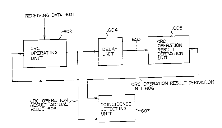
Figure 6 is a block diagram for explaining the
principle of the present invention;
Figure 7 shows a principle configuration for
explaining the preferred embodiment of the HEC
synchronizing circuit of the present invention;
Figure 8 shows the first example of a circuit
configuration of a CCR;
Figure 9 is an operational timing chart for
25 explaining the principle configuration of the
20~2~5~
preferred embodiment;
Figure 10 shows the second example of a circuit
configuration of a CCR;
Figure 11 shows a practical configuration for
explaining the preferred embodiment of the HEC
synchronizing circuit associated with the present
invention;
Figure 12 is an operational timing chart for
explaining an example of a practical configuration of
the present invention;
Figure 13 shows a view for showing for each
initial value an operation result obtained in a CRC
operation performed on a header part using an initial
value having only one value "1" in its 8 bits.
Description of the preferred embodiments
Explanation of the Principle
Figure 6 is a block diagram for explaining the
principle of the present invention, and shows an HEC
20 synchronizing unit for detecting errors in the header
part of a cell in the asynchronous transfer mode (ATM)
switching method and for performing a cell
synchronizing operation.
A CRC operating unit 602 performs a cyclic
2~ redundancy check (CRC) in which received data 601 are
- 1 1
divided by a predetermined generated polynomial with a
CRC operation result actual value 603 obtained in the
previous operation as an initial value in response to
received data 601 applied in a byte unit. Then, it
5 outputs the CRC operation result actual value 603 as a
remainder.
A delay unit 604 delays the output of the CRC
operation result actual value 603 by the time in which
a header part of the received data 601 takes to be
10 inputted.
A CRC operation result derivation unit 605
outputs a value as a CRC operation result derivation
value 606 as if it were obtained as a result of a CRC
operation performed for all the receiving data of a
15 header part including a CRC code of the length of the
above described header part using as an initial value
the CRC operation result actual value 603 outputted by
the delay unit 604. The unit 605 comprises a
plurality of logical circuits for outputting a value
20 as a CRC operation result derivation value 606 as if
it were obtained as a result of a CRC operation
performed for all the receiving data of a header part
including a CRC code of the length of the above
described header part using an initial value having
25 one bit value different from the values of the other
20~285~
12
bits. Each logical circuit is provided for each
initial value having a different value bit placed at a
different position. Each of the logical circuits is
connected such that the CRC operation result
5 derivation value 606 can be obtained as an exclusive
logical sum of output values of the logical circuits
each corresponding to an initial value having a
different value at a different bit position .
A coincidence detecting unit 607 compares the CRC
10 operation result actual value 603 outputted by the CRC
operating unit 602 with the CRC operation result
derivation value 606 outputted by the CRC operation
result derivation unit 605. It then detects the input
timing of received data containing no errors in the
15 header part provided with a CRC code.
The above described configuration of the present
invention relates to an HEC synchronizing unit in the
ATM switching method. However, the present invention
is not limited to this application, but can be used to
20 detect the segmentation of data containing a CRC code
by sequentially performing a CRC operation for
detecting errors in data.
In the present invention, when a CRC operation is
performed for a header part containing a CRC code (the
25 header part can comprise common data to be processed)
2 13
and when an initial value does not comprise all "Os"
but may have other bit configurations, the operation
result of the CRC operation of the header part takes a
unique value in response to the initial value. Thus,
the CRC operation result derivation unit 605
(corresponding to the CCR) performs a deriving
operation to derive as the CRC operation result
derivation value 606 an operation result in response
to any initial value.
Based on the above described condition, the CRC
operating unit 602 performs a CRC operation for each
piece of sequentially received data in a byte unit,
and the CRC operation result actual value 603 obtained
by each CRC operation is used as the initial value of
the next CRC operation.
In the above described configuration, the CRC
operation result actual value 603 obtained in the CRC
operation performed on the 5th byte (in the HEC
portion) of a 5-byte header part is equal to the CRC
operation result derivation value 606 derived by the
CRC operation result derivation unit 605 using the
initial value used when a CRC operation is performed
for the byte four bytes before the present one, that
is, the first byte of the header part. The initial
value is equal to the CRC operation result actual
2~62855
14
value 603 obtained in the CRC operation performed for
the 5 bytes before the present byte.
In the present invention, the delay unit 604
delays the CRC operation result actual value 603 by 5
5 bytes corresponding to the data length of a header
part, for example. Then, the CRC operation result
derivation unit 605 derives the CRC operation result
derivation value 606 as if it were obtained as a
result of a CRC operation performed for the whole 5-
10 byte header using as an initial value the CRCoperation result actual value 603 for the data 5 bytes
before the present received data 601 (data to be
processed ) in the present CRC operation. Thus
obtained CRC operation result derivation value 606 is
15 compared with the CRC operation result actual value
603, the input timing of receiving data containing no
errol~s in a header part can be detected as the timing
indicating "coincidence" between these values, thus
establishing the HEC synchronization.
Explanation of the Preferred Embodiment
A preferred embodiment of the present invention
is described below in association with the attached
drawings.
The general configuration of the ATM switching
206285S
unit related to the preferred embodiment of the
present invention is the same as that shown in Figure
1. The block configuration of a transmission line
terminal unit 102 (Figure 1) for realizing an HEC
synchronizing operation is the same as that shown in
Figure 3. The feature of the preferred embodiment
described below resides in a practical configuration
of the HEC synchronizing circuit 301. Before
explaining the configuration, the operational
principle of the preferred embodiment is described.
In the prior art technology shown in Figure 4,
one-byte data comprising all "Os" are applied as an
initial value to the first CRCC 401, and an operation
result of a CRC operation in each of the CRCCs 401 is
provided to the next CRCC 401. The input timing of a
5-byte header part is detected with the operation
result in the 5th CRCC 4015 obtained as "0". Thus, in
the prior art technology, since an initial value must
be set as all "Os", five CRCCS for performing a CRC
operation in a byte unit must be connected, and the
hardware is thus configured in a large scale.
By contrast, in the present invention, a result
of a CRC operation for a 5-byte header part (a
remainder of a division in which the 5-byte data of a
header part is divided by a generated polynomial using
2062855
16
the above described initial value) is uniquely
obtained in response to an initial value when a CRC
operation is performed for a 5-byte header part and
when an initial value in the operation does not
comprise all "0s" but any other initial values.
Figure 13 shows results of operations in which
only one bit in an initial value comprising eight
bits, that is, one byte, contains "1" when a CRC
operation is performed for a 5-byte header part.
Using Figure 13, a result of a CRC operation
performed for a 5-byte header part can be derived when
an initial value can be any value. That is, in any
initial value comprising 8 bits, a bit indicating the
value "1" is extracted, and an operation result of an
initial value having the above described bit as the
only bit containing the value "1" is extracted from
Figure 13. A result of a CRC operation performed on a
5-byte header part comprising the above described
initial value can be derived as a value sequentially
indicating exclusive OR for each bit in each operation
result. For example, when an 8-bit initial value is
"OOlOOlO1", the O-th, 2nd, and 5th bits indicate "1".
Therefore, a result of a CRC operation for a 5-byte
header part can be derived as the value "lOOO1001"
obtained by sequentially calculating an exclusive
206~85~
logical sum for each bit of the operation results
"01100010", "10001111", and "01100100" obtained in
(a), (c), and (f) in Figure 13.
The present preferred embodiment is based on the
above described fact. That is, a CRC operation is
performed on each piece of sequentially received 1-
byte data, and a result obtained in each CRC operation
is used as the initial value of the next CRC
operation. In this configuration, the result obtained
in the CRC operation performed for the 5th byte of a
5-byte header part (an HEC portion) is equal to the
operation result derived according to Figure 13 for
the initial value used when a CRC operation is
performed on the byte four bytes before the present
one, that is, the first byte of the header part. The
initial value is equal to the result of the CRC
operation for the byte 5 bytes before the present one.
In the present preferred embodiment, a circuit is
provided to derive a value as if it were obtained as a
result of a CRC operation performed for a 5-byte
header part using as an initial value the result of
the CRC operation for the data which is 5 bytes before
those to be processed in the present CRC operation.
The input timing of the 5th byte of the header part,
that is, the HEC portion, is detected as the timing at
--- 2062855
^ 18
which the derivation result and the result of the CRC
operation for the data being processed are equivalent.
The synchronization of a header part can thus be
established.
Figure 7 shows the principle for explaining the
- present preferred embodiment for realizing the above
described operations. Receiving data 705 sequentially
applied in a byte unit from an ATM transmission line
101 (Figure 1) are temporarily stored in the FF7040
and then applied to a CRC operating circuit (CRCC)
701.
The CRCC 701 performs for the receiving data 705
applied in a byte unit from the FF7040 a CRC operation
in which the above described receiving data 705 are
divided by the generated polynomial x8 + x2 + x + 1
using as an initial value a CRC operation result
actual value 706 obtained in the previous CRC
operation, and then it outputs as a remainder an 8-bit
CRC operation result actual value 706.
The CRC operation result actual value 706 is
delayed by 5 input timings by the five serially
connected FF 7041 - 7045, and applied to a CRC code
correcting circuit ( CCR ) 702.
The CCR 702 outputs a value as an 8-bit CRC
operation result derivation value 707 as if it were
--- 20~285S
1~
obtained as a result of a CRC operation performed for
a 5-byte header part using as an initial value the CRC
operation result actual value 706 outputted by the
CRCC 701 5 input timings before the present process
timing, that is, the initial value used in the CRCC
701 which is 4 input timings before the present
process timing.
A coincidence detecting circuit 703 compares the
8-bit CRC operation result actual value 706 outputted
by the CRCC 701 with an 8-bit CRC operation result
derivation value 707 outputted by the CCR 702. If all
corresponding bits of these values coincide, a
determination output 708 indicating coincidence is
outputted.
The FF 7040 - 7045 operate according to a clock
CLK synchronized with the input timing of the received
data 705. In this case, if the transmission speed of
the ATM transmission line 101 shown in Figure 1 is 600
Mbps, for example, the input speed of a byte (8 bits)
can be calculated as:
600 / 8 = 75 Mbps
where 75 MHz indicates the clock frequency.
In Figure 7, the actual circuit configuration of
the CRCC 701 is the same as that shown in Figure 5 and
described above in the prior art technology.
2062855
Next, Figure 8 shows the first typical
configuration sample of a circuit. As shown in Figure
8, the CCR 702 comprises a plurality of exclusive
logical sum elements (EOR). Bit signals cO - C7 (MSB
on the side of C7) corresponds to each bit of the CRC
operation result actual value 706 inputted to the FF
7045 shown in Figure 7 and outputted from the CRCC 701
5 input timings before the present process timing,
that is, each bit of the initial value in the CRCC 701
4 input timings before the present process timing.
Bit signals Do - D7 correspond to each bit of the CRC
operation result actual value 706 shown in Figure 7.
Each of 8010 ~ 8017 enclosed in dotted lines
performs a conversion process indicated by (a) - (h)
shown in Figure 13. For example, the 8010 is a
circuit unit for outputting "01100010" when the O-th
bit cO of an initial value indicates "1" and the 1st
bit cl to the 7th bit C7 indicate "O". An exclusive
logical sum is sequentially obtained in a bit unit for
each operation result shown in Figure 13 by connecting
each of the portions 8010 - 8017 enclosed in dotted
lines through an exclusive logical sum element as
shown in Figure 8. Basically, an exclusive logical
sum element is applied to the bit position where "1"
is outputted by a corresponding portion 801 enclosed
--- 2~6~855
21
in dotted lines according to Figure 13. A byte data
applied to the portion 8017 comprise all "Os" as shown
in Figure 8.
Figure 9 shows an operational timing chart for
explaining the principle configuration of the present
preferred embodiment shown in Figures 5, 7, and 8.
The receiving data 705 are entered in a byte unit as
shown by (a) of Figure 9 after synchronized with the
clock CLK, having a frequency of 75MHz, for example,
as shown by (b) of Figure 9. Then, the data are
stored by the FF 7040 at the rise timing of the clock
CLK, and the output is applied to the CRCC 701 at the
timing shown by (c) of Figure 9. At the same timing,
the CRC operation result actual value 706 is outputted
from the CRCC 701 to the coincidence detecting circuit
703. At the same timing again, the content of the CRC
operation result derivation value 707 is outputted
from the CCR 702, and it is a derivation value
corresponding to the CRC operation result actual value
706 outputted from the CRCC 701 5 input timings before
the present process timing as shown by (d) of Figure
9. For example, by (c) of Figure 9, the following
values can be obtained at the timing at which the 5th
byte of a header part, that is, the portion BHEC of
the HEC, is applied to the CRCC 701. a53 shown by (d)
~ 2062855
22
of Figure 9 can be obtained from the FF 7045 as the
CRC operation result actual value 706 at 5 inputs
timing before the present process timing corresponding
to A53, that is, the 53rd byte (last byte) of the
previous cell of the present cell. Also, the CRC
operation result derivation value 707 corresponding to
a53 can be obtained from the CCR 702. If there are no
errors in the data of the header part, a determination
output 708 indicating coincidence is outputted by the
coincidence detecting circuit 703.
As described above, in Figure 4, five CRCCs 401
must be serially connected, while, in Figure 7, only
two circuits comprising one CRCC 701 and another CCR
702 of the same scale are required, and the circuit
scale can thus be reduced.
Next, Figure 10 shows the second example of a
circuit configuration. In the above described first
example of the circuit configuration shown in Figure
8, the portions 8010 ~ 8017 enclosed in broken lines
can be connected in any order according to the
characteristics of an exclusive logical sum. In the
portion 8017 enclosed in broken lines, each exclusive
logical sum element is omitted. At its bit position,
five exclusive logical sum elements can be omitted if
an initial value C7 is directly applied to the next
206~5~
23
portion 801 enclosed in broken lines. Thus, as shown
in Figure 10, a CCR 702 can be configured with the
smallest possible number of elements, and the circuit
scale can thus be further reduced.
Figure 11 shows a practical configuration for
explaining the preferred embodiment of the HEC
synchronizing circuit 301 shown in Figure 3 of the
present invention. The basic configuration and
operation are the same as those of Figure 7. In
Figure 11, the CCR 1102 corresponds to the CCR 702
shown in Figure 7; the coincidence detecting circuit
1103 corresponds to the circuit 703 shown in Figure 7;
the FFs 11040 ~ 11045 correspond to the FFs 7040 -
7045; the receiving data 1105 correspond to the data
705 shown in Figure 7; the CRC operation result actual
value 1106 corresponds to the value 706 shown in
Figure 7; the CRC operation result derivation value
1107 corresponds to the value 707 shown in Figure 7;
and the determination output 1108 corresponds to the
output 708 shown in Figure 7. The configuration of
Figure 11 differs from that of Figure 7 in that it
comprises only two CRCCs 11011 and 11012, two
additional FFs 11047 and 11048 for retaining each
B output, an AND element ~ , and an exclusive logical
element~. The configuration of the preferred
2062855
24
embodiment shown in Figure 11 follows the circuit
configuration according to the CCITT recommendations.
According to the CCITT recommendations related to
the ATM switching method, an exclusive logical sum is
calculated with each bit of a CRC code obtained as a
CRC operation result and each bit of a code called
"coset" indicating "01010101", and the operation
result is stored as an HEC in the header part of a
cell according to the recommendations when on a
sending side of a cell a CRC operation is performed
for 4-byte header data and a l-byte HEC is added to
the data. Therefore, on the receiving side, an
exclusive logical sum is calculated again for the HEC
portion with the receiving data 1105 outputted by the
lS FF 11040 and the above described coset "01010101" to
decode the original CRC code, and then perform a CRC
operation. The exclusive logical sum element 611 and
CRCC 11012 shown in Figure 11 are provided to perform
the necessary processes involved. The exclusive
logical sum element 611 is used as an element to
obtain an exclusive logical sum for each bit using 1-
byte (8-bit) receiving data 1105 provided by the FF
11040 and 8-bit coset "01010101".
Figure 12 is an operational timing chart for
explaining the practical configuration of the
206285~
preferred embodiment shown in Figure 11. For example,
the 5th byte of a header part, that is, the HEC
portion BHEC~ is outputted at the timing shown by (e)
of Figure 12. The exclusive logical sum element 611
subtracts a coset from the HEC data, and they are
inputted to the CRCC 11012. At the next timing at
which a bHEC shown by (f) of Figure 12 is outputted as
a CRC operation result true value 1109 by the FF
11048, an a53 shown by (h) of Figure 12 corresponding
to A53, the 53rd byte (last byte) and the previous
cell of the present input cell, is obtained as a CRC
operation result actual value 1106. At the same
timing, a CRC operation result derivation value 1107
corresponding to the above described a53 can be
obtained by the CCR 1102. If no errors have arisen in
the data of the header part, a determination output
1108 indicating a coincidence is outputted by the
coincidence detecting circuit 1103.
As described above an appropriate process can be
performed for an HEC provided with a coset.
The configuration shown in Figure 11 differs from
that shown in Figure 7 in a clock for operating each
FF 1104. In the preferred embodiment shown in Figure
11, a transmission method called SONET is used in the
ATM transmission line 101 shown in Figure 1.
206~
Therefore, in the preferred embodiment shown in Figure
11, a signal component of a pulse OH indicating
overhead of the SONET is subtracted from an AND
element 610. The resultant clock FF CLK operates each
FF 1104. In this configuration, as shown in (a) of
Figure 12, no FF 1104 continues its operation if the
receiving data 1105 equals the overhead of the SONET.
AS described above, in the practical
configuration of the preferred embodiment shown in
Figure 11, an HEC synchronizing circuit 301 (Figure 3)
can be realized in conformity with the CCITT
recommendations related to the ATM switching
method.