Note: Descriptions are shown in the official language in which they were submitted.
2062~70
71493-41
The invention is in the field of telephony
communications and particularly relates to a telephone line
powered interface between a digital signals telephone line and a
computer communications line.
Various practices of using telephone facilities as a
means of providing communications links for digital signal devices
such as digital telephones, telemeter apparatus, digital computers
and the like, are well known. Digital telephone facilities of the
time division multiplex (TDM) type have been utilized to advantage
to provide usable bandwidth of up to 64 Kb/s for example, for
computer communications. Of course appropriate interface devices
are required to transfer control and data signals between the
operating formats of the telephone line of the telephone system
and a communications port of the computer. One class of computers
generally referred to as Personal Computers (PC) is exemplary, as
such computers are often in an isolated situation where the only
practical means of electronic communications is via a telephone
connection. Some manufacturers of personal computers have made
general provision for unforseen requirements by providing
connection locations for additional circuit devices as and when
required. In such an instant an appropriate telephone line
interface circuit may reside in such a location and advantageously
make use of support facilities already resident in the computer,
such as power supplies for example. As the purpose of the
telephone line is that of communicating at a distance from the
telephone facility it is only natural the interface with the port
of the computer be provided closely adjacent the computer and
2062870
71493-41
preferable by circuit means installed within the computer for this
purpose. However in some instances the provided space may already
be occupied or there may never have been any space provided in a
particular module of PC. In such instances the interface device
must reside independently of the computer and be connected thereto
by a typical standardized computer communications port. Such
ports are usually operable in one of several well known standards,
RS-232, RS-422 and RS-423 for example. Furthermore such ports are
not usually adapted to operating over distances similar to those
distances over which typical telephone lines are usually
operative. The telephone line may be operable in the standard
analog format, the integrated services digital network format
(ISDN), or in any of several proprietary formats. In any case the
interface device is unlikely to have access to the computer as a
source of operating power and therefor some other provision for
operating power is required.
One example of an interface device is discussed in the
United States Patent No. 4,381,427 issued on April 26, 1983 to
W.E. Cheal et al and titled "Subscriber Loop System for voice and
data". In this patent, the interface device requires more
operating current than is available to it via the telephone line.
In order that a local utility power failure be of no consequence
to the normal operation of the telephone system, a relay
switchover feature is provided so that at least plain ordinary
telephone service (POTS) may continue in spite of such power
failure. In most modern telephone systems all seems well checks
as to the operability of lines and telephone apparatus
2062`870
perlodlcally occur. In Cheal et al's arrangement, a local
power fallure ls prevented from dlsruptlng the normal all
seems well malntenance checks to the operatlng advantage of
the telephone switch. Presently personal computers are
usually adapted such that data calls may be originated or
answered for example, via the computer key board, and hence
the telephone apparatus as provided by Cheal is not essential.
Examples of commercially available integrated
circuit devices used to provide this type of lnterface are
*Motorola MC1488, MC1489, 26LS31 and 26LS32. These devlces
obtain their operating power from the control switch of the
telephone switchlng system. Recently, however, telephone
swltchlng systems, such as the *Norstar system developed by
Northern Telecom Llmlted, have been proposed in which the
current which is available to the remote device is too low to
run such commercially available device. The Norstar system is
described in TELESIS, Volume 16, Number 2, published by Bell-
Northern Research Ltd. ln 1989. On the other hand, some
commercial interface devices are available which operate with
sufflclent low current consumptlon but they can only operate
at up to 20 Kblts/sec, whlch ls much less than the 450
Kblts/sec requlred by some lndustry deslgns.
It ls an ob~ect of the invention to provide an
lnterface devlce which ls remote from an assoclated telephone
faclllty and whlch is lndependent of any local powerlng source
such as a utlllty powered supply for lts operatlon.
- 3 -
~L) * Trade-mark 71493-50
2062870
71493-41
More specifically, it is an object of the invention to
provide a telephone line powered interface device which couples
information signals between a serial digital signal format of the
telephone line and any of a plurality of standard port operating
formats of a personal computer.
According to one broad aspect, the invention provides an
interface circuit for converting first digital data in which
binary "l"s and "O"s are defined by first and second voltage
levels respectively into a data signal in which the binary "l"s
and "O"s are defined by third and fourth voltage levels,
respectively, the interface circuit comprising a first current
source deriving a voltage at the third voltage level and a second
current source deriving a voltage source at the fourth voltage
level and means for connecting the first current source to an
output when the digital data is at the first voltage level and for
connecting the second current source to the output when the
digital data is at the second voltage level.
In another aspect, the invention provides an interface
circuit for converting first digital data in which binary "l"s are
defined by a first voltage ranging between a first two levels and
binary "O"s are defined by a second voltage ranging between a
second two levels into a data signal in which the binary "l"s and
"O"s are defined by third and fourth voltage levels, the interface
circuit comprising a level translator and inverter for setting an
output voltage to the third voltage level when the incoming
voltage is between the first two levels and for setting the output
2062870
voltage to the fourth voltage level when the lncomlng voltage
ls between the second two levels.
According to yet another aspect, the lnvention
provides an interface circuit for connecting a telephone
interface unit in which digital data represented by +5V for
logic "1" and OV for logic "0" is present to a personal
computer in which logic "1" ls represented by a negative
voltage having a numerical value of at least 5 volts and loglc
"0" is represented by a positive voltage having a numerical
value of at least 5 volts, the interface unit comprising a
transmltter clrcuit having a first current source connected to
+5V and a second current source connected to -5V and means for
connectlng the flrst current source to the computer when the
dlgital data is OV and connecting the second current source to
the computer when the digital data is +5V, the interface unit
further comprising a receiver circuit for producing an output
voltage of +5V when data received from the personal computer
is a negative voltage having a numerical value of at least 5
volts and for producing an output voltage of OV when data
recelved from the personal computer is a positlve voltage
havlng a numerlcal value of at least 5 volts.
In a specific embodiment, the negatlve voltage
representlng a loglc "1" ln the computer ls ln the range -5V
to -12V and the positive voltage representing a loglc "0" ln
the computer ls in the range +5V to +12V.
The invention will now be descrlbed ln greater
detail with reference to the accompanying drawings in which:
Figure 1 is a block diagram showing a telephone
-~., 71493-50
2062870
switchlng system in whlch telephone sets and personal
computers are connected to a central swltch;
Flgure 2 ls a block dlagram of one of the lnterface
unlts shown ln Flgure 1 and lllustratlng the lnterconnectlon
of the lnterface unlt between the central swltch and a
personal computer;
Flgure 3 ls a functlonal block dlagram lllustratlng
the operatlon of a custom llne lnterface clrcult formlng part
of the lnterface unlt of Flgure 2;
Flgure 4 ls a clrcuit dlagram of the custom llne
lnterface clrcult;
Flgure 5 ls a block dlagram lllustratlng ln greater
detall a power supply block formlng part of the clrcultry of
Flgure 2; and
Flgure 6 ls a block dlagram lllustratlng ln greater
detall a data transmlt/recelve block and a data translator
block formlng part of the clrcultry of Flgure 2.
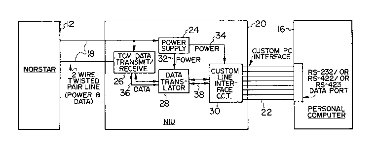
A Norstar system 10, shown ln Flgure 1, comprlses a
Norstar central swltch 12 connected to Norstar telephone sets
14 and to personal computers 16. The llnk between each set 14
and the central swltch 12 ls a two wlre twlsted pair llne 18.
However, ln the case of each P.C. 16, the llnk lncludes, ln
addltlon to a two wlre twlsted palr 18, an lnterface unlt 20
connected to the central swltch by the twlsted palr 18 and
connected to the P.C. 16 by means of an 8 wlre cable 22.
Referrlng now to Flgure 2, whlch shows one of the
lnterface unlts 20 ln greater detall, the lnterface unlt 20
comprlses a power supply 24, a TCM (Tlme Compresslon
71493-50
2062870
Multiplexed) data transmlt/receive block 26, a data translator
28 and a custom llne lnterface clrcult 30. The lnterface unlt
20 ls, as lndlcated above, connected to the central swltch 12
by a two wlre twlsted palr whlch carrles both power and data.
- 6a -
71493-50
2062870
71493-41
The power supply 24, described in greater detail
hereinafter with reference to Figure 6, receives power from the
Norstar central switch 12 over the associated two wire twisted
pair 18 and converts this into a form suitable for the data
translator 28 and the custom line interface 30. More
particularly, the power supplied from the central switch 12 is
approximately 19 volts DC and this is converted by the power
supply 24 to +5 volts DC and -5 volts DC for powering the data
translator and custom line interface circuits over lines 32 and
34, respectively.
The TCM data transmit/receive block 26 receives from and
transmits data to the central switch 12, the data being in the
form of time compression multiplexed (TCM) data. This is a
proprietary data format of Northern Telecom and is characterized
by high speed half duplex data transmission. In this type of data
transfer, known as "ping pong", the data travels in only one
direction at a time but the direction is rapidly alternated so
that data transfer is accomplished in both directions. In the TCM
data transmit/receive block 26 the TCM data is converted into
standard digital data (+5V representing a logic "1" and OV
representing a logic "0"). Of course, in the reverse direction
standard digital data is converted into TCM data for transmission
along wire pair 18 to the central switch 12.
The data translator 28 is connected to the TCM data
transmit/receive block 26 via a data link 36 along which the
standard digital data passes and to the custom line interface
circuit 30 via a data link 38. The data translator 28 converts
2062870
71493-41
the standard digital data into a form which is acceptable to
personal computers. The data is then arranged into words of 8
bits in length (or 1 byte in length) and is encoded in such a way
that the personal computer can accept it. The data is encoded in
either an asynchronous manner or a synchronous manner depending on
the operating mode of the interface unit 20. The asynchronous
mode is the standard "universal asynchronous receive/transmit" or
UART mode which most personal computers accept. The synchronous
mode is a clocked format where the data is synchronized to an edge
of a clock signal.
The custom line interface circuit 30 provides the
physical interface between the interface unit 20 and the personal
computer 16. It consists of two separate types of circuit: a
receiver circuit and a transmitter circuit. The transmitter
circuit converts the standard digital data from the data
translator 28 into data voltage levels required by the personal
computer. The receiver circuit converts the data voltage levels
coming from the personal computer into standard digital data
required by the data translator 28.
Specifically, the transmitter circuit converts the
standard digital data (+5V for a logic "1" and OV for a logic "0"~
from the data translator 28 to -5V for a logic "1" and +5V for a
logic "0". The receiver circuit converts data coming from the
personal computer which is between -5V and -12V for a logic "1"
and between +5V and +12V for a logic "0" into the standard digital
data.
2062870
71493-41
Figure 3 shows conceptually how the custom line
interface circuit 30 works. The top half of the Figure shows a
representation of a transmitter circuit 40 and the bottom half
shows a representation of a receiver circuit 42.
The transmitter circuit converts the standard digital
data (+5V for logic "1" and OV for logic "0") into the data levels
required by the personal computer (-5V for a logic "1" and +5V
for a logic "0"). It does this by controlling connection to two
current sources by means of an electronic switch 43. When the
digital data is +5V, a current source 44 to the -5V power rail is
switched in. This results in the output line to the personal
computer being pulled down to the -5V level. When the digital
data is OV, a different current source 46 to the +5V power rail is
switched in. This results in the output line to the personal
computer being pulled up to the +5V level. Since only one current
source is on at any one time very little power is used. The
conventional way of doing this would be to have the +5V current
source 46 on always but have the -5V current source 44 stronger
and able to overpower the +5V current source. This results in a
waste of power whenever the -5V current source is turned on.
The receiver circuit converts the data from the personal
computer (between -5V and -12V for a logic "1" and between +5V and
+12V for a logic "0"). into standard digital levels required by
the data translator 28. (+5V for logic "1" and OV for logic "0").
It does this by a level translator circuit 48 and an inverter
circuit 50. The level translator circuit 48 clamps the incoming
voltage to +5V when the signal from the personal computer 16 is
2062870
71493-41
between +5V and +12V, i.e., for an incoming logic "0". Similarly,
the level translator circuit 48 clamps the incoming voltage to 0V
when the signal from the personal computer is between -5V and -
12V, i.e., for an incoming logic "1". The inverter circuit 50
then simply inverts the signal (i.e., +5V output for 0V input and
0V output for +5V input) which completes the receiver function.
Figure 4 is a circuit diagram of the custom line
interface 30. This comprises essentially the components for two
of the transmitter circuits 40 and two of the receiver circuits 42
illustrated conceptually in Figure 3. Typical values for the
resistors and capacitors used in Figure 4 are indicated.
Figure 4 illustrates the connections made between the
custom line interface 30 and the eight wires of cable 22. These
interconnections are established at pins numbered 1-8 formed at an
edge of interface unit 20. Specifically, the two transmitter
circuits 40 are connected, respectively, to pins 5 and 2 and the
two receiver circuits 42 are connected, respectively, to pins 1
and 3. Additionally a +5V signal is applied through resistor ~13
to pin number 7, two signal grounds are connected, respectively,
to pins 4 and 8 and pin number 6 is left floating.
One of the transmitters 40 and one of the receivers 42
carries the actual data from or to the twisted pair 8. The other
transmitter and receiver are used for "handshaking" signals
between the interface unit 20 and the personal computer 16 which
can have different functions depending on the application. For
example, the personal computer 16 could pull its handshaking
signal to a particular logic level to signal that it cannot accept
20~2870
714g3-41
any more data from the interface unit 20. Alternatively the
interface unit 20 may pull its handshaking signal to a particular
logic level to signal that it cannot accept any more data from the
personal computer 16. The exact use of these handshaking signals
depends on the application and does not have any direct bearing on
the present invention.
One transmitter circuit is formed principally of
resistors R5, R6, R11, capacitor C1, transistor Q1, comparator U2A
and inverters UlC and UlD. The other transmitter circuit is
formed principally of resistors R7, R8, R12, capacitor C2,
transistor Q2, comparator U2B and inverters UlE and U2F.
Resistors R9, R10 and capacitor C3 are shared between the two
transmitter circuits. Only the first transmitter circuit will be
described as the configuration and operation of the second is
identical.
Resistor R5 connects the emitter of transistor Q1 to a
+5V bias. Inverter UlD has an input to which is supplied the
standard digital data signal referred to as "MACOUT" in both
Figures 3 and 4. Inverter UlC is serially connected to the
parallel combination of resistor R6 and capacitor C1, this
parallel combination in turn being serially connected to the base
of transistor Q1. The input of inverter UlC is connected to the
output of inverter UlD.
The output of inverter UlD is also connected to the +
input of comparator U2A the output of which is connected to the
collector of transistor Q1 from which collector the output signal
RXDA - to the personal computer 16 is taken at pin 5. The - input
2062870
71493-41
of comparator U2A is connected to the junction of resistors R9,
R10 and capacitor C3.
Components R5 and Q1 form the +5V current source 46.
This current source is turned on or off by the digital voltage
level at the output of inverter UlC. When the output of inverter
UlC is high (+5V) the current source is turned off when the output
of inverter UlC is low (OV) the current source is turned on.
Components R6 and C1 are tailored to control the speed at which
the current source is turned on and off.
The -5V current source 44 is provided by the comparator
U2A. When the + input of comparator U2A is at a lower voltage
level than the - input the output is connected to -5V and thus the
current source is turned on. When the + input of comparator U2A
is at a higher voltage level than the - input the output is
floating which means the current source 44 is turned off. The
comparator U2A is an "open collector' device meaning its output
can only go low (to -5V in this case) and is otherwise out of the
circuit. The components R10 and R9 provide a resistor divider
network to place +2.5V at the - input of U2A. This provides a
bias which the digital signal (either 0V or +5V) at the + input is
compared with. Capacitor C3 is used to filter any noise which
might be present on the 2.5V bias signal.
Overall, the transmitter circuit operates as follows:
When the input signal called "MACOUT" is at a digital
"1" (+5V), the signal at the + input of comparator U2A is OV since
it was inverted by inverter UlD. Thus the output of comparator
U2A is -5V. As well, the output of inverter UlC is +5V which
2062870
71493-41
turns the +5V current source 46 consisting of Q1 and R5 off. The
output signal to the personal computer at pin 5 is then -5V.
When the input signal called "MACOUT" is at a digital
"0" (OV~, the signal at the + input of comparator U2A is +5V since
it was inverted by inverter UlD. Thus the output of comparator
U2A is off and essentially out of the circuit. The output of
inverter UlC is then 0V which turns the current source 46
consisting of Q1 and R5 on. The output signal to the personal
computer at pin 5 is then +5V.
The receiver circuit converts the data from the personal
computer (between -5V and -12V for a logic "l" and between +5V and
+12V for a logic "0") into standard digital levels required by the
data translator 28. (+5V for logic "1" and 0V for logic "O").
One receiver circuit is formed principally of resistors
R1, 2R, schottkey diodes D1, D2 and inverter UlA, which typically
is a CMOS 74HC14 device. The other receiver circuit comprises
B resistors R3, R4, diodes D3, D4 and inverter ~. Only the first
receiver circuit will be described as the configuration and
operation of the second is identical.
The incoming signal from the personal computer is
applied to the pin 1 labelled "HSKOa". This voltage is current
limited by R1 (20K ohms) and applied to the schottkey diodes D1
and D2. The schottkey diodes clamp the voltage at the input to
inverter UlA to a minimum of -0.3V and a maximum of +5.3V since
the diodes have an on voltage of approximately 0.3V and are
connected to the +5V and ground supply voltage rails.
2062870
71493-41
Thus when the incoming voltage at the "HSKOa" pin 1 is
between +5V and +12V (which it will be for an incoming logic "O"),
the voltage at the input of inverter UlA will be between +5V and
+5.3V. This is inverted by inverter UlA and the output signal
(labelled "DTR") will be OV.
When the incoming voltage at the "HSKOa" pin 1 is
between -5V and -12V (which it will be for an incoming logic "1"),
the voltage at the input of UlA will be approximately -0.3V. This
is inverted by inverter UlA and the output signal (labelled "DTR")
will be +5V.
Resistor R2 (300K ohms) is provided to ensure that the
voltage at the input of inverter UlA does not float when there is
no personal computer connection to pin 1. This is necessary since
CMOS devices such as the 74HC14 should not have floating inputs or
excessive power supply current may be drawn. When no personal
computer is connected to pin 1, resistor R2 pulls the input of UlA
to OV.
The power supply 24, described with reference to Figure
2, will now be described in greater detail with reference to
Figure 5.
The power supply block 24 receives power from the
Norstar central switch 12 over the 2 wire twisted pair 18 and
converts this into +5V DC and -5V DC which is required by the
other circuitry in the interface unit 20.
The 2 wire twisted pair 18 has a differential voltage of
between lOV DC and l9V DC on it from the central switch 12. This
voltage is rectified by a schottkey diode bridge 60 to ensure the
14
2062870
71493-41
proper polarity of voltage to a switching regulator 62. The
B switching regulator 62 used is a Siliconix~SI9100 device. This
device converts the 10V C to l9V DC voltage into a pulse width
modulated AC signal. This AC signal is applied to a transformer
T2 "DRIVE" winding. Transformer T2 is composed of four windings
on a common core as shown. One of the transformer windings is the
"SENSE" winding. It is used to provide a feedback signal to the
switching regulator. By monitoring the sense winding the
switching regulator is able to adjust the pulse width modulated
"DRIVE" signal accordingly. The "DRIVE" signal is adjusted to
maintain the transformer output signals. The output signals from
transformer T2 are rectified and filtered by two diodes 64 and two
electrolytic capacitors 66 to provide the +5V and -5V DC voltages.
The data transmit~receive block 26 and the data
translator block 28, both described with reference to Figure 2,
will now be described in greater detail with reference to Figure
6.
This block receives and transmits TCM data from the
Norstar over the 2 wire twisted pair 18 via a jack 68. The TCM
data is in an AC form which is suitable for transmission over a
long twisted pair wire.
The TCM data is transformer coupled by transformer Tl
and applied to the input pins of a Northern Telecom Custom LSI
device 70. (Referred to as "CLSI"). This CLSI device 70 converts
the TCM data (half duplex AC format) into standard digital type
data. The digital data is characterized by a logic level of +5V
for a data "1" and 0V for a data "0". The standard digital data
~r~J~ ~L 15
2062870
71493-41
is presented to the data translator block from the CLSI in a
synchronous serial format from a serial interface 72 which is
connected to the data translator via four wires which together
form the data link 36. The four wires are TX (transmit data from
CLSI 70), RX (receive data from data translator block 28), CLK
(clock to define when data is valid), and SYN (Synchronization
pulse which defined the first bit in the bitstream).
The CLSI 70 has a microprocessor interface 74 through
which an external microprocessor in the data translator block 28
is able to monitor and control the operation of the CLSI 70.
The purpose of the data translator block 28 is to
transform the serial data from the CLSI 70 to a form which is
acceptable to personal computers. Both an asynchronous and
synchronous personal computer data format are supported. The
asynchronous format is the standard "universal asynchronous
receivettransmit" or UART format. The synchronous format is the
"high level data link control" or HDLC format. The HDLC format is
a clocked data format where the receive and transmit data is
synchronized to a clock signal.
The data translator block 28 is composed of a National
Semiconductor Corporation HPC46400 microprocessor device 76 plus
EPROM 78 and RAM 80 memory. The EPROM memory (electrically
programmable read only memory) is used for program storage. The
RAM (random access memory) is used for temporary data storage.
The HPC 46400 microprocessor 76 has many chip functions which
facilitates the movement of data. These functions include a
direct memory access (DMA) controller 82, a UART 84, an HDLC
~' 7 raJ~ 16
2062870
71493-41
controller 86 and a serial interface 88 which is compatible with
the Northern Telecom CLSI serial interface.
The DMA controller is used to automatically move data
between the serial interface and the external RAM and also between
the external RAM and the HDLC controller. In this way, data can
be routed between the HDLC port and the serial interface by being
temporarily buffered in the RAM. Data can also be moved between
the serial interface and the UART by being temporarily buffered in
RAM. An input port 90 is also provided and a microprocessor bus
94 which provides interconnection between microprocessor 76 and
the interface 74 as well as with the EPROM 78 and the RAM 80.
The UART 84 provides the asynchronous serial data
receiver and transmitter function. The UART 84 formats data into
a serial word composed of a start bit, 8 data bits and a stop bit.
Most personal computers are able to communicate in this
asynchronous mode. As shown in the figure, input data to the UART
is labelled "MACIN" and output data from the UART is labelled
"UARTOP".
The HDLC controller 86 provides the synchronous serial
data receiver and transmitter function. The HDLC controller 86
formats data into a serial bit stream with a clock signal to
define when data is valid. Many personal computers are able to
communicate in this synchronous mode. Referring to the figure,
input data to the HDLC controller is labelled "MACIN" and output
data from the HDLC controller is labelled "MACOUT". The HDLC
controller clock signal is labelled "MACCK".
2062870
71493-41
The signal DTR is a handshake signal. This signal is
set either high or low by the personal computer to signify a
certain condition. The DTR signal is read by the HP46400
microprocessor 76 via the input port 90.
The interface unit 20 incorporating the novel custom
line interface circuit 30 of the present invention is able to
operate satisfactorily with very low power consumption at speeds
up to 450 Kbits/sec with personal computers operating under RS232,
RS422 or RS423 standards for up to 8 feet of cable between the
computer and the interface.
The use of a low power LM393 comparator device for the
-5V current source also contributes to the low power nature of the
transmitter circuit.
Typical industry standard devices (such as Motorola
MC1488 devices) have internal transistor circuits which require
much more power to operate than the LM393 device.
Another aspect of the low power nature of the device is
the receiver circuit. The receiver utilizes a 74HC14 CMOS
(complementary metal oxide semiconductor) device for inverter UlA
(or UlB). This is a digital CMOS device which has very low power
consumption. These digital CMOS devices are not typically
employed as line receiver circuits. Typical receiver devices
(such as Motorola MC1489 devices) use bipolar transistor circuits
which require much more power to operate. The reason digital CMOS
devices are not typically used in line receiver circuits such as
this one is that the CMOS devices cannot tolerate large voltages
at their inputs. This invention however uses diodes and resistors
18
2062870
71493-41
to limit the voltages at the CMOS devices input to an acceptable
level. (For example, diodes D1 and D2 and resistor R1 are used
for CMOS device UlA in Figure 4).
19