Note: Descriptions are shown in the official language in which they were submitted.
2062~3i
- 1 - 41PR-6901
SWITCHBOARDS AND PANELBOARDS
HAVING INTERLOCK AND LOAD SELECTION CAPABILITIES
BACKGROUND OF THE INVENTION
U.S. Patent Application Serial No. 674,475 entitled
"An Electronic Circuit Interrupter with Attached
Terminal ~onnector Board~ describes a main circuit
breaker connected within a switchboard enclosure
containinq a plurality of branch circuit breakers. The
main and branch circuit breakers each include
individual terminal blocks that are arranged within the
switchboard enclosure. The main and branch circuit
breakers communicate with a central programming unit
over a power-line communication network to provide
supplemental protection features.
The branch circuit breakers described within the
aforementioned U.S. Patent Application are so-called
"smart" circuit breakers wherein each circuit breaker
contains its own microprocessor and software support
programs. The terminal boards connected with the
individual circuit breakers provide the means for
connecting with the power-line communication link that
connects the central programming unit with the main and
2~62931
- 2 - ~lPR-6901
branch circuit breakers.
With Zone-Selective-Interlock function, wherein an
upstream circuit breaker is restrained from responding to
interrupt a protective circuit until a downstream circuit
breaker closer to the source of the fault has responded,
there must be some means for cOD unicating betwesn the
upstream and downstream circuit breakers.
U.S. Patent 4,468,714 entitled "Zone Selective
Interlock Module for Use with Static Trip Circuit
Breakers" describes one such Zone-Selective-Interlock
system using hard-wired connections between the upstream
and downstream circuit breakers.
"Load Selection" as described herein concerns
prioritizing the electrical equipment loads that are
connected with distributed branch circuit breakers
whereby selected circuit breakers are actuated to
interrupt operating power to non-essential eguipment
while the operating power to those circuit breakers
connected with essential equipment such as computers,
emergency lighting and medical apparatus is maintained.
U.S. Patent 4,672,501 entitled "Circuit Breaker and
Protective Relay Unit" describes a "smart" circuit
breaker which includes a microprocessor programmed to
perform the Load Selection function.
U.S. Patent 4,589,052 entitled "Digital I2T Pickup,
Time Bands and Timing Control Circuits for Static Trip
Circuit 8reakers" describes an electronic trip unit
useful for overcurrent protection, which does not include
a microprocessor. When such electronic trip units are
used as branch circuit breakers it would be highly
advantageous to provide such circuit breakers with
Zone-Selective-Interlock and Load Selection Functions.
U.S. Patent 4,991,042 entitled "Digital Circuit
_ 3 _
Interrupter with Keypad Data Entry and Display" describes
a smart circuit breaker containing its own miaroprocessor
and associated circuitry for entering trip parameters to
the electronic trip unit and displaying the trip
parameters along with voltage and ampere ratings, upon
command.
Accordingly, one purpose of the invention is to use a
smart circuit breaker as the main circuit breaker within
a switchboard or panelboard enclosure along with a
plurality of distributed branch circuit breakers
containing electronic trip units such as described in the
- aforementioned U.S. Patent 4,589,052.
SUMMARY OF THE INVENTION
A smart circuit breaker containing a micraprocessor
within its electronic trip unit is arranged as a main
circuit breaker within a switchboard or panelboard
enclosure. A plurality of branch circuit breakers
containing electronic trip units without a microprocessor
are electrically interconnected with the microprocessor
within the main circuit breaker.
Zone-Selective-Interlock and Load Selection functions are
provided by operation of the shunt trip and auxiliary
switch accessories contained within the branch circuit
breakers.
BRIEF DESCRIPTION OF THE DRAWINGS
Figure 1 is a front plan view of a switchboard or
panelboard enclosure containing a main circuit breaker
and distributed branch circuit breakers interconnected in
accordance with the invention;
Figure 2 is a top perspective view of the main
circuit breaker used within the switchboard or panelboard
2062931
- 4 - 41PR-6901
enclosure of Figure l;
Figure 3 is a top perspective view in isometric
projection, of one of the branch circuit breakers used
within the switchboard or panelboard enclosure of Figure
1;
Figure 4 is a schematic representation of the
electronic trip unit used within the branch circuit
breaker depicted in Figure 3;
Figure 5 is a schematic representation of the
lo electronic trip unit used within t~e main circuit breaker
depicted in Figure 2;
Figure 6 is a diagrammatic representation of the main
and branch circuit breakers depicted within the
switchboard or panelboard enclosure of Figure 1 connected
in a double-branch arrangement;
Figure 7 is a flow chart representation of the
control program used with the main and branch circuit
breakers within the switchboard or panelboard of Figure
l;
Figure 8 is a flow chart representation of a
Zone-Selective-Interlock program used with the main and
branch circuit breaker within the switchboard or
panelboard of Figure 1 when the main circuit breaker is
in the short-time pick-up mode;
Figure 9 is a flow chart representation of the Load
Selection program and Zone-Selective-Interlock program
used with the main and branch circuit breakers within the
panelboard or switchboard of Figure 1, when the main
circuit breaker is in the long-time pick-up mode: and
Figure 10 is a flow chart representation of the Load
Selection program used with the main and branch circuit
breakers within the panelboard or switchboard of Figure
1 ~
2062931
- S - 41PR-6901
DESCRIPTION OF THE PREFERRED EM~ODIMENT
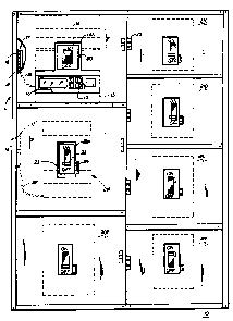
A switchboard or panelboard 10 of the type consisting
of an extended metal enclosure 11 is shown in Figure 1
and includes a plurality of closed compartments 12 that
are accessible by means of a compartment handle 25. One
of the compartments contains a main circuit breaker 13
similar to that described in the aforementioned U.S.
Patent 4,991,042 and includes a handle 14 extending from
a handle escutcheon 14A and a keypad 15 along with a
display 16. The handle, keypad and display are
accessible through an inverted T-shaped slot 20 formed
within the front surface of the compartment. As
described within the aforementioned U.S. Paten~
Application Serial No. 674,475 the main circuit breaker
is connected to a terminal board 17 by means of a cable
19. The main terminal board includes a plurality of main - -
terminals 18 that interconnect with corresponding branch
terminals 18' associated with similar branch terminal
boards 17'. The branch terminal boards each connect with
one of the branch circuit breakers 21A by means of a
similar cable 19'. The branch circuit breakers are
similar to those described within U.S. Patent 4,754,247
entitled "Molded Case Circuit Breaker Accessory
Enclosure". Each of the branch circuit breakers has an
operating handle 22 extending from the handle escutcheon
22A along with the trip-test button 24 which are both
accessible through a slot 23 formed through a front
surface of the compartment. Similar branch circuit
breakers 21B-21F are located within the remaining closed
compartments.
The main circuit breaker 13 i8 best seen by referring
now to Figure 2 wherein the main circuit breaker contains
a ca~e 26 to which a circuit breaker cover 27 is fixedly
2~2931
- 6 - 41PR-6901
attached and which includes an accessory cover 28
attached to the circuit breaker cover. The keypad 15 and
display 16 described within the aforementioned U.S.
Patent 4,991,042 are arranged under a protective plastic
plate 29 and can be accessed for inputting and displaying
the trip parameters by first removing the protective
plate. As described in the aforementioned U.S. Patent
Application Serial No. 674,475 the terminal board 17 is
connected to the load end of the main circuit breaker
cover by means of the multi-conductor cable 19.
Electrical connection with the electronic trip unit
contained within the main circuit breaker cover is made
by means of the terminals 18. For purposes to be
described below in greater detail, the terminals 18 are
allocated to the branch circuit breakers (21A-21F) by
designating the terminal connectors 100 (A-F), 101 (A-F)
and 102 (A-F) accordingly wherein the letters ("A-F")
designate the (A-F) branches of the protected power
circuit and the numerals (100-102) designates the Pick-Up
(P.U.), Shunt Trip (S.T.) and Auxiliary Switch (A.S.)
connectors. The group of terminal connectors 100 (A-F)
designated "P.U." are allocated for connection with the
pick-up indication terminals from electronic trip units
within each of the associated branch circuit breakers.
The group of terminal connectors 101 (A-F) designated
~S.T. n are allocated for connection with corresponding
branch circuit breaker terminals connecting with the
actuator-accessory units 33 (Figure 3) contained within
the branch circuit breaker covers. The group of terminal
connectors 102 (A-F) designated "A.S." are allocated for
connection with corresponding branch circuit breaker
terminals connecting with the auxiliary switch units 40
(Figure 3) contained within the branch circuit breaker
2062931
- 7 - 4lpR-6s
covers. Terminal connector 103 connects with systems
ground.
One of the branch circuit breakers 21A is depicted in
Figure 3 prior to final assembly. The branch circuit
breaker has a similar case 26, cover 27 and accessory
cover 28 as the main circuit breaker, described earlier
and common reference numerals for both the main circuit
breaker and branch circuit breaker components will be
used where possible. An actuator-accessory unit 33 of
lo the type described within U.S. Pate~t 4,894,631 is
positioned within the accessory-actuator recess 33A and
interacts with the circuit breaker operating mechanism
(not shown) by means of the actuator latch 34. The
actuator-accessory unit responds to signals generated by
the electronic trip unit 37 within the trip unit recess
37A over wire conductor 35 to articulate the circuit
breaker operating mechanism and separate the circuit
breaker contacts (not shown). The actuator-accessory
unit also responds to trip signals generated from a
remote location over the shunt-trip wire conductor 36
that passes under the branch circuit breaker through a
slot 67 and then upwards within a wiring channel 43
formed within the case 26. The shunt-trip wire conductor
passes through the multi-conductor cable 19 to the branch
terminal board 17' and is electrically connected to one
of the terminal connectors designated (lOlA) "S.T". The
operation of the actuator-accessory unit 33 as a
shunt-trip aCCe850ry i8 described within U.S. Patent
4,858,056 entitled "Molded Case Circuit Breaker
Actuator-Accessory Module". The electric circuit for
controlling the operation of the actuator-accessory
module as a shunt-trip accessory is found within U.S.
Patent 4,860,157 entitled "Molded Case Circuit Breaker
2062931
- 8 - 41PR-6901
Actuator-Accessory Module". An auxiliary switch
accessory 40 is inserted within an auxiliary switch
recess 40A also formed within the branch circuit breaker
cover 27. The auxiliary switch interacts with the branch
circuit breaker operating mechanism by means of an
actuator lever 41 to provide a signal over the auxiliary
switch wire conductor 42 which passes through an opening
(not shown) in the bottom of the auxiliary switch recess
40A to the wiring channel 43 and then out to the branch
terminal board 17' via cable 19. The auxiliary switch
wire conductor 42 connects with another one of the
terminal connectors designated (102A) "A.S.". The
electronic trip unit 37 in the circuit breaker cover 27
electrically connects with the branch terminal board 17'
by means of the pick-up indicator wire conductor 46 which
exits through the bottom of the auxiliary switch recess
40A and the wiring channel 43 out through the cable 19
and connects with the end of the terminal designated
(lOOA) "P.U.". The terminal connector 103 similarly
connects with systems ground as described earlier. A
rating plug 30 is inserted within the rating plug recess
30A formed in the accessory cover 28 and electrically
connects with the trip unit 37 by means of sockets 38
formed on the bottom of the rating plug and upstanding
pins 39 formed on the trip unit 37. The accessory cover
28 is securely fastened to the branch circuit breaker
cover 27 by means of machine screws 68, thru-holes 69 and
threaded openings 70 as indicated. Access to the
actuator-accessory unit 33 is made by means of the
accessory door 31 and access to the auxiliary switch 40
is made by means of the other accessory door 32. The
remaining branch circuit breakers 21B-21F also have
similar terminals 18 containing corresponding terminal
.;~ . ,
. .
20~293~
- 9 - 41PR-6901
connectors 100 (~-F) "P.U.", 101 (B-F) "S.T." and 102
(i3-F) "A.S." respectively.
The trip unit circuit 58 used within the trip unit 37
is depicted in Figure 4 include~ an integrated circuit
trip unit 49 similar to that described within the
aforementioned U.S. Patent 4,589,052. The trip unit
connects with the multi-phase power conductors 55 and
associated current transformers 56 through a signal
conditioning circuit 47. The signal conditioning circuit
includes a rectifier 50 wherein the.current signals are
changed to a DC configuration and applied across the
rating resistor Rb for providing circuit current data to
the trip unit over wire conductor 71. The signal
conditioning circuit includes a power supply 51 that
derives its operating power from the current transformers
and which inputs operating power to the trip unit over
conductor 72. As fully described within aforementioned
U.S. Patent 4,589,052, a trip actuator circuit 48
controls the condition of the circuit breaker contacts 57
that are serially connected within the multi-phase power
conductors 55. A trip output signal from the trip unit
controls the driver circuit 54 which connects with the
trip coil 52 through an SCR 53 to separate the circuit
breaker contacts upon the occurrence of an overcurrent
condition of predetermined duration through the
multi-phase power conductors. The pin connectors (1-3)
on the trip unit connects with an externally accessible
switch over conductor 73 to vary the instantaneous and
short-time trip parameters stored within the trip unit.
Pin connector 4 connects with terminal connection lOOA
(P.U.) on the branch terminal board 17' over conductor 46
(Figure 3) for providing information as to the occurrence
of a long-time or short-time overcurrent condition
206293~
- 10 - 41PR-6901
occurring on the multi-phase power conductors in a manner
to be discussed below in greater detail.
The trip unit circuit 59 depicted in Figure 5 is used
within the trip unit contained within the main circuit
breaker 13 shown earlier in Figure 2 and includes a
microprocessor 60 that connects with a similar signal
conditioner circuit 47 and trip actuator circuit 48 to
separate the circuit breaker contacts 57 serially
connected within the multi-phase power conductors 55.
The current data through the multi-phase power conductors
is transmitted to the microprocessor by means of the
current transformers 56, signal conditioner circuit 47
and the wire conductors 64 as indicated~ As fully
described within the aforementioned U.S. Patent 4,991,042
the operational programs for the microprocessor are
stored in the ROM 62 and the trip parameter values are
stored in the RAM 61 both of which connect with the
microprocessor I/O ports 24, 25 by means of the 12 BIT
address and 8 BIT data buses 63, 64. I/O ports 1-6
connect with the externally accessible keypad switches 15
(Figure 2) to enter and display the trip parameters
stored within the RAM 61. I/O ports 7-12 connect with
the corresponding pick-up indicating tenninal connectors
100 (A-F) "P.U." on the branch terminal boards 17'
connected with the branch circuit breakers 21 (A-F) shown
in Figures 1 and 3. The I/0 ports ~13-18) connect with
the corresponding branch shunt trip terminal connectors
101 (A-F) "S.T." and the I/0 ports (19-24) connect with
the corresponding branch auxiliary switch terminal
connectors 102 (A-F) "A.S" in a manner to be described
below in greater detail.
A double-branch circuit arrangement 66 for the main
circuit breaker 13 and branch circuit breakers (21A-21F)
2062931
`- -- 11 -- 41PR-6901
(Figure 1) is depicted in Figure 6. Branch circuit
breaker 2lA protects branch circuit A which in turn
connects in series with branch circuits C, D as
indicated. Branch circuit breaker 2lB protects branch
circuit ~ which connects in series with branch circuits E
and E. The branch circuits (C-F) each include
corresponding branch circuit breakers (21C-21F~.
The Zone-Selective-Interlock function (Z.S.I.) and
Load Selection function (L.S.) for the branch circuit
breakers (21A-21F) can be seen by referring now to
Figures 2, 3, 5 and 6. The main terminal 17 of the main
circuit breaker 13 of Figures 1 and 2 is arranged such
that each of the branch terminal connectors 100 (A-F)
"P.U.", lO1 (A-F) ~S.T.", and 102 (A-F) "A.S.'i connects
with a corresponding main terminal 18 on the main
terminal board 17. The Z.S.I. function iæ performed as
follows. Upon occurrence of an overcurrent condition
within one of the branch circuit breakers 21C, for
example, in Figure 6, the appropriate signal of the
pick-up indication is transmitted from the associated
branch terminal board 17' to the main terminal board 17.
The microprocessor can then delay operation of the main
circuit breaker and activate the actuator-accessory unit
within the branch circuit breaker 2lC by outputting a
shunt trip signal over the appropriate I/0 port (13-18)
to articulate the operating mechanism and separate the
contact~ within the branch circuit breaker 2lC. The
auxiliary switch unit within the branch circuit breaker
21C then closes and outputs an auxiliary switch signal
indication to the microprocessor over the appropriate I/0
port (19-24) to indicate to the microprocessor that the
branch circuit breaker 2lC has responded to interrupt the
fault. The Z.S.I. ~unction accordingly deters the
` 20629~1
- 12 - 41PR-6901
operation of the upstream branch circuit breaker to allow
the downstream branch circuit breaker closest to the
fault to interrupt the circuit current.
The L.S. function is performed by assigning the
branch circuit breakers 21C, 21D, 21E and 21F a priority
with respect to operation. Critical equipment such as
emergency lighting, computers and medical equipment are
prioritized and peripheral equipment such as air
conditioners and machinery are shut down before the
critical equipment. When the total current through the
branch circuit breakers 21C and 21D exceeds the rating of
the upstream branch circuit breaker 2lA, a pick-up
indication signal is transmitted to the appropriate I/0
port (7-12) on the microprocessor 60. The microprocessor
then determines whether the downstream circuit breakers
21C, 21D are also experiencing an overcurrent condition.
If not, the nonessential equipment is interrupted by
actuating the associated actuator-accessory unit in the
non-prioritized branch circuit breaker 2lC or 2lD. The
appropriate auxiliary switch siqnal is transmitted by the
branch circuit breaker to the appropriate I/0 port
(19-24) to signify to the microprocessor that the
selected branch circuit breaker has responded.
The instructions to the microprocessor for performing
the Z.S.I. functions are depicted in the flow chart
diagram 75 as shown in Figure 7. Upon start-up, the
microprocessor is initialized (76) and inquiry is made as
to whether the main circuit breaker is in pick-up (77).
If it is determined that the main circuit breaker is in
pick-up an inquiry is made as to whether the trip time
delay in the main circuit breaker electronic trip unit is
started (78). If not, the trip time delay is begun (79).
If the trip time delay in the main circuit breaker is
. . ,
. ' .
2062931
- 13 - 41PR-6901
started, inquiry is made as to whether the trip response
of the main circuit breaker is inhibited (80) and if not,
whether the time delay is over (81). If the trip
function within the main circuit breaker is inhibited,
inquiry is made as to whether the pick-up mode is
short-time (83). If the time delay is over, the
electronic trip unit within the main circuit breaker is
initiated, the main circuit breaker is tripped (82) and
the loop is continued by again determining whether the
main circuit breaker is in pick-up. If the time delay is
not over, the control program continues along branch 84
or branch 85 depending upon the magnitude of the
overcurrent condition in the main circuit breaker.
The short-time delay operating program (84) is
depicted in Figure 8 and determines whether the A branch
breaker is in pick-up (86) and if so, a shunt trip signal
is inputted to the trip unit of the ~ branch breaker to
trip the A branch breaker (87) and inquiry is made as to
whether the ~ branch breaker is in pick-up (88). If it
2 0 i8 determined that the A branch breaker is not in
pick-up, and the ~ branch is in pick-up then the shunt
trip signal is inputted to the trip unit within the B
branch breaker (89). If the ~ branch breaker is not in
pick-up, the trip inhibit to the main circuit breaker is
cancelled (90).
The long-time operating program 85 is depicted in
Figure 9 and begins with an inquiry as to whether the A
branch breaker is in pick-up (91). If so, the trip unit
within the main circuit breaker is inhibited (92). If
the ~ branch breaker is not in pick-up an inquiry is made
as to whether the ~ branch breaker is in pick-up (93).
If the ~ branch breaker is in pick-up, the main breaker
trip unit i8 inhibited (92) and the loop is continued.
2062931
- 14 - 41PR-6901
If the ~ branch breaker is not in pick-up, the main
circuit breaker trip unit inhibit is cancelled (94) and
an inquiry is made as to whether the contacts in the A
branch breaker are closed (95). If the contacts in the A
branch breaker are closed, a shunt-trip signal is
inputted to the trip unit within the A branch breaker
(~8). If the contacts in the A branch breaker are not
closed, inquiry is made as to whether the contacts in the
B branch breaker are closed ~96). If the contacts in the
lo B branch breaker are closed, a shunt-trip signal is
inputted to the trip unit within the B branch breaker
(97).
The branch Load Selection programs controlling the
microprocessor 60 of Figure 5 for the main and branch
circuit breakers depicted earlier in Figure 6 are
depicted in Figures 7 and 10 as follows. When it is
determined that the main breaker is not in pick-up (77)
the branch load select flow diagram (104) is initiated
whereby an inquiry is made as to whether the A branch
circuit breaker is in pick up (105) and if so, whether
the C branch circuit breaker is in pick-up (106). If the
C branch circuit breaker is not in pick-up, an inquiry is
made as t~ whether the D branch circuit breaker is in
pick-up (107) and if not, a shunt trip signal is inputted
to the trip unit within the D branch circuit breaker
(108). If the A branch circuit breaker is in pick-up and
either the C branch circuit breaker or the D branch
circuit breaker is in pick-up, then inquiry is made as to
whether the B branch circuit breaker is in pick-up. If
the ~ branch circuit breaker is not in pick-up, inquiry
is made as to whether the B branch circuit breaker is in
pick-up (109) and if so, inquiry is made as to whether
the ~ branch circuit breaker is in pick-up (110). If the
-`~ 206293~
- 15 - 41PR-6901
~ branch circuit breaker is not in pick-up, inquiry is
made whether the E branch circuit breaker i8 in pick-up
(111) and if not, a shunt trip signal is inputted to the
trip actuator within the E branch circuit breaker (112)
If the ~ branch circuit breaker is in pick-up, or the E
branch circuit breaker i8 in pick-up, the loop is
continued
It has accordingly been shown that a "smart" circuit
breaker e~ploying a microprocessor and related ROM and
RAM memory can include internal operational programs and
external terminal connections with circuit interrupters
having an electronic trip unit and an electrically
actuated accessory-actuator unit When a plurality of
such elQctronic circuit break r~ are connected within a
common enclo~ure, the a~ociated t-rminal connector
boards are int-rconn cted with the smart circuit breaker
in a "master-~lave~ relation wh-reby the ~mart circuit
br-aker control~ the tripping s-guence of the branch
circuit breakers for Zone-Sel-ctive-Interlock and Load
S-lection functions