Note: Descriptions are shown in the official language in which they were submitted.
WO 91/00523 ; PCT1US90/03639
_ 1 _ 2063~~8w .~
PORTABLE LOW POWER COMPUTER
10 FIELD OF THE INVENTION
This invention relates to small low power computers,
--- in particular battery operated computers using liquid
crystal displays.
BACKGROUND OF THE INVENTION
Personal computers have become faster and smaller in
recent years. Desktop computers typically use household
power and run commercially available software written for
execution through an operating system such as MS-DOS~
(MS-DOSS is a registered trademark of Microsoft
Corporation) or Unix~ (Unix~ is a registered trademark of
American Telephone & Telegraph). In addition to the
computing unit, these computers include a monitor for
displaying information to the user and a keyboard for
receiving information from the user. They may include
disk drives, a printer, a communications modem, and may
include even more peripheral devices. Since the computer
must be compatible with commercially available software, a
basic input/output system (BIOS) which is unique for each
' computer converts commands generated by the operating
system or application program to specific machine commands
- implemented by the hardware of the machine. These
computers include an internal clock which operates
continuously when the machine is turned on and controls
the central processor to access memory, load registers,
WO 91/005 ~ ~ ~~ ~~ ~ , PCT/US90/03639
_ 2
read and write to disk, detect keyboard use, and control a
display, all operations synchronized with cycles of the
internal clock. In addition, if the computer accesses an
external port, the external commLwications may be
controlled by an asynchronous clock through a UART
(universal asynchronous receiver/transmitter). The power
used by these desk-top wall-plug computers has not been of '
particular concern because it is small when compared with
power used by other appliances which also use the same
power source.
Methods for reducing power used by a computer have
included using CMOS circuitry, and using liquid crystal
display monitors rather than cathode ray tube monitors or
plasma display technology. - - w
There exists a class of small, lightweight computers
which have been designed for low power and may use
batteries. These computers do not have the computing
capability of a desk top machine nor the ability to run
the full range a commercial software and operating systems
available for desk top machines. They typically have
reduced display resolution and inconvenient keyboards.
Another class of computers generally described as lap
top computers are battery operated, portable, and may run
a broad range of commercial software. However, these lap
top computers are powered by bulky rechargeable batteries
and can only operate for a few hours before requiring the
batteries to be recharged.
SUMMARY OF THE INVENTION
The present invention provides a computer combining
many features which allow the computer to occupy a small
space and allow for operation of the computer using
considerably lower power than that of the lap top
computers presently available, and yet which has the
computing power of a desk-top IBM XT or AT and a display
monitor which can display 80 characters by 25 lines. A
test of one XT compatible computer shows a battery life of
CA 02063558 1999-08-11
3
about 100 hours of operation with two AA alkaline batteries. A
preferred embodiment uses standard batteries widely available, so
that this computer can continuously serve a user travelling to
remote parts of the world. that is, spare batteries can be
easily carried (a single AA size battery, for example, is less
than two inches long and one inch thick) and may be purchased
widely just as are batteries used in most flashlights and
portable radios. The preferred embodiment could use any battery
which met the form factor of the compartment and had the same
approximate electrical specifications. Another embodiment could
use a battery other than AA size batteries.
Thus, the computer operates effectively on inexpensive
batteries that, as in the example of AA batteries, initially
provide about 1.6 volts, and as they are drained later provide
only about .8 volts. Prior art computers require batteries that
provide a level amount of voltage during their useful lives.
In a preferred embodiment the computer is housed in a
two-part low profile rectangular case hinged along one long edge
and latched at an opposite edge. The hinge extends along a back
edge of the case and rotatably joins upper and lower portions of
the case. The case is preferably of a plastic such as
polycarbonate and/or ABS plastic or both. The case is of molded
constructions.
A lower portion of the case includes a keyboard, one or
two memory cards, batteries, and most of the integrated circuit
components of the computer. The integrated circuit components in
this lower portion are attached to the lower side of a printed
circuit board which occupies most of the rectangular area
encompassed by the case. Included in these integrated circuit
components are two
CA 02063558 1999-08-11
4
ASIC (application specific integrated circuit) chips. In order
to conserve space, particularly vertical space, these ASIC chips
are put on the board without the usual packaging. Such packaging
(which is omitted) would include a plastic or ceramic protective
cover surrounding a lead frame which connects interior pin-outs
to exterior pins. The unpackaged chip is bonded directly to the
lower printed circuit board, thereby saving both horizontal and
vertical space in the present very compact structure. The
microprocessor chip is also attached directly to the printed
circuit board without intervening packaging, which reduces
connection points and cost.
Also attached to the lower side of this printed circuit
board are connectors for receiving removable memory cards,
preferably at least two connectors for two cards. These
connectors are the same thickness as the card itself. No circuit
components are located on that part of the printed circuit board
adjacent to where the memory cards are placed, so that the memory
cards fit within the existing envelope of the computer housing.
At one or several edges of the printed circuit board
are pads to which traces extend from pins of the integrated
circuit chips to which test signals are applied during
manufacturing. These pads are accessed with edge connectors
which are designed to slip over an edge of the board and make
electrical contact with the pads. This avoids the need for
applying test probes to the interior of the circuit board and
thereby saves time and avoids testing mistakes.
The upper side of the same printed circuit board in the
lower portion of the case serves as a back plate for the
keyboard. Traces for electrically detecting each key
WO 91/00523 , , PCT/US90/03639
- 5 - ~~~~~63~~5
state are applied directly to the upper side of this
printed circuit board. The keyboard includes a keyplate
through which extend a plurality of keys. The keys press
corresponding' cones in an insulating flexible membrane,
each cone including a conductive flexible pad which in a
compressed position spans conductive traces on the printed
circuit board and in a non-compressed position leaves
these conductive traces unconnected.
The keyboard occupies most of the inner surface of
the lower case, occupying more than half, and preferably
70% or more of the surface area of the inner surface of
the lower case.
The upper side of this printed circuit board also
------ ---includes traces for detecting a machine reset. As a novel
feature of the present invention, reset is activated by
inserting a pointed object such as a pencil point through
an opening in the keyboard and pressing an electrically
conductive pad rather than by pressing a key or
combination of keys.
As another novel feature of the present invention,
one of the keyboard keys is an on/off toggle key. The
computer never turns completely off, but in the off state
operates only a low frequency clock which keeps time-of-
day.
After testing of the lower printed circuit board and
installation of the membrane during assembly of the
computer, the keyplate which holds the keys in position is
welded to the lower portion of the case in order to
achieve accurate registration of the keys, the membrane,
and the traces.
Located between the hinge and the keyboard area is a
compartment including batteries and a capacitor. This
capacitor is sufficient to maintain volatile memory with
the computer in the off state while batteries are being
changed. The batteries are covered by a plate which is
imprinted with descriptions of a top row of keyboard
function keys, these function keys being located just
CA 02063558 1999-08-11
6
adjacent to the battery cover plate. In one embodiment, four
notations in four different colors are imprinted on the cover
plate adjacent each function key. Keys for "shift", "alt",
"ctrl", and a special logo key are correspondingly colored to
indicate to a user that combining the "shift", "alt", "ctrl", or
the logo key with the adjacent function key produces the function
noted in color adjacent the function key. Alternate cover
plates, tapes for attaching to the cover plate, or cards for
placing adjacent this cover plate may be provided for use with
different software packages.
An upper portion of the case houses a liquid crystal
display plus a separate power supply for the liquid crystal
display. In one embodiment a space is provided between the
display and the outside of the upper case for insertion of a
display back light powered by separate batteries or other power
source. The liquid crystal display occupies most of the entire
area enclosed by the upper portion of the case, with a narrow
frame surrounding the liquid crystal display and its cover.
The display when displaying characters shows 25 lines
of 80 characters per line. A line of characters is typically 8
pixels tall so that the standard 25 lines of text are displayed
using 200 rows of pixels. Additionally, a status line using one
or more rows of pixels at the top, bottom or both, of the display
are provided for showing status of various software programs and
hardware conditions. Coordinating with these displayed status
lines are imprinted legends along the top, bottom, or both
margins of the display frame for indicating to the user the
meanings represented by these status lines. As with the
keyboard, different legends can be provided for different
software packages.
CA 02063558 1999-08-11
7
Since separate power supplies are located in the two
portions of the computer case, the number of current carrying
lines which must extend between the upper and lower housing is
minimized. A cable including these lines extends from the lower
to the upper portion of the case and is located toward the
interior of the computer from the hinge axis. The cable has
sufficient length to span from its lower point of connection to
its upper point of connection when the computer case is fully
open. The spiral design of the cable acts as a spring so that
when the computer is closed, the excess cable slack is taken up
in a cable cover located in the upper or lower portion of the
case, preferably lower. This cable cover protects the cable from
excess flexure, assuring long life.
This arrangement of the components allows for the
computer to fold to a very compact size for being carried and to
open to a convenient size in which the two components which
interface with the user, namely the keyboard and the display, are
large enough to be convenient. To further reduce thickness, the
keys are made so that some keys are pressed by the display upon
closing the computer case. Preferably, these are the front
(lower) row of keys.
In one embodiment, the keyboard is controlled such that
a multiplicity of key presses does not cause an executing program
to cease operation. The on/off key is a key not depressed when
the case is closed. When the
1
WO 91 /00523 PGT/US90/03639
;;, ~,.,
2D6~3'~~g' ~ - 8 -
on/off key is pressed to toggle the computer to its off
state, other keys are deactivated such that pressing the ,
other keys upon closing the case is not detected by the
computer. When the computer is in this off state, the
processor does not lose its place in the program Which was
running. All memory remains static but execution is
halted until the machine is moved out of the off state.
While in this off state, timer interrupts are processed
allowing time of day updating, and allowing software which
uses the time of day interrupt to process the interrupt.
The computer of the present invention includes a
power management system which maintains as many components
of the computer in an off state for as much time as
- -- - possible even when the computer is on. Individual
components can be turned off while other components remain
on. Components of the machine which can be turned off
while the machine appears to a user to be on include the
oscillator and clock which cycle the central processor,
another oscillator and clock which control the display, a
direct memory access (DMA) clock tied to the central
processor oscillator which controls direct memory access
circuits, and an oscillator and clock for communication to
an external port. While the machine is turned on, that
is, while the display is on and the machine is responding
to user input, the hardware detects activities f or which
some parts of the machine can be turned off. These clocks
can actually be turned off while the user is in the midst
of executing a program. For example, when a user is
executing a word processing program, the clock which
controls the central processor is turned off for most of
the time between one keystroke and the next.
In a preferred embodiment, four activities are
monitored for determining when parts of the machines can be
turned off: the state of the on/off switch, keyboard
presses, software activity and clock ticks generated by a
low frequency clock and a divider circuit. When these
activities are not occurring, certain clocks and devices
CA 02063558 2000-04-25
70128-229
9
driven by the clocks are turned off. Because in a preferred
embodiment CMOS circuitry is used, which uses most of its power
when switching, turning off oscillators and their associated
clocks greatly reduces power consumption of the system.
Turning off devices themselves also reduces power.
The invention may be summarized as a compact portable
computer including a keyboard, the keyboard comprising: a
keyplate having a plurality of keys and a printed circuit board
underlying and held in a spaced relation to said keyplate, said
printed circuit board having two surfaces, a first surface
bearing conductive traces for detecting key presses of the keys
of the keyplate, and an opposing second surface having most of
the integrated circuit components of the computer mounted
thereon, thereby providing a compact portable computer
keyboard.
According to another aspect the invention provides a
computer system comprising; a main processor integrated circuit
of the computer system; a full function alphanumeric keyboard
for inputting data into said main processor; a display device
for outputting data from said main processor; and a printed
circuit board, one side of said printed circuit board having
said main processor integrated circuit mounted thereon and the
other side of said printed circuit board bearing conductive
traces for detecting key presses of said keyboard.
BRIEF DESCRIPTION OF THE DRAWINGS
Figure 1. Perspective view of the computer.
Figure 2. Exploded view of keyboard.
CA 02063558 2000-04-25
70128-229
9a
Figure 3. System diagram showing interconnections of
the integrated circuit chips.
Figure 4. A circuit board, front side.
Figure 5. Circuit board of Figure 4, rear side.
Figures 6A, 6B. Attachment of IC's to a circuit
board.
Figure 7. A test structure.
Figures 8A, 8B. A computer reset structure.
Figure 9. A border plate, display and keyboard.
Figures 10A to lOCe. Schematics of a peripheral
ASIC.
Figures 11A to llAd. Schematics of a system ASIC.
Appendix A is an I/0 map.
Identical reference numbers in various figures refer
to identical or similar structures.
DETAILED DESCRIPTION OF SOME PREFERRED EMBODIMENTS
Overview of System Components
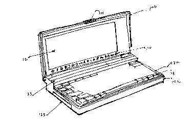
Fig. 1 shows a perspective view of the computer
showing upper case 110a, lower case 110b, display 112, display
frame 113, keyboard 118, key plate 118a, battery
WO 91/00523 r , PCT/US90/03639
~ o s 3~:~:~ s~
.., - 10 -
cover 123, hinge 111, latch 114, memory card tray 125, and
display indicator graphics 130.
Fig. 2 shows an exploded view of the computer
keyboard 118 showing keyplate 118a with keys such as 181,
182, and 183, membrane 128 with cones such as 281, 282,
and 283 each holding a conductive pad (not shown), and
printed circuit board 138. '
Membrane 138 is elastomeric, and protrudes upward in
a plurality of locations to form a plurality of
elastomeric cones, one beneath each key, for example cones
281, 282, and 283 beneath keys 181, 182, and 183
respectively. Each cone is truncated at a flat (or
relatively flat) upper surface which is contacted by an
underside of its corresponding key.-~Extending downward
from the flat upper surface of each of the elastomeric
cones into the interior of the respective cone is an
elastomeric conductive pill. When a key is pressed, its
corresponding cone is compressed, moving its corresponding
pill into position to span conductive traces (not shown)
on the printed circuit board 138. ,
Figure 4 shows a first side of the printed circuit
board 138 including IC chip mounting areas 302, 304, 306.
Figure 5 shows the rear (i.e., second) side of the
printed circuit board 138 including key contacts such as
310, 312, etc. to which conductive traces such as 318,
320, etc. are connected.
Figure 6A shows in a side view how one IC chip 340 is
electrically connected to printed circuit board 138 by
bond wires 342, 344, etc. from pins 346, 348, etc. on chip
340 to bonding pads 350, 352 on printed circuit board
138. IC chips such as 340 thus preferably do not have the
usual lead frame packaging. Figure 6B shows a top view of
Figure 6A.
Figure 7 shows a test structure as provided on
printed circuit board 138. As shown, five separate test ...
interconnect areas are provided, 360, 362, 364, 366, 368,
each consisting of several pads such as 370, 372 to which
WO 91/00523 PCT/US90/03639
- 11 - 2 ~ ~ 3 ~'~'8~ v' ''
test signals are provided by test cables such as 380.
Test cable 380 is connected to printed circuit board 138
only when testing is to be performed. Card edge test
connector 382 connects test cable 380 to the pads 370,
372, etc. As shown, indicating locator such as 390, 392
are provided as cut outs in the edge of printed circuit
board 138 to locate the card edge test connectors such as
382. Note that as shown in Figures 4 and 5, such a test
structure is provided on both sides of printed circuit
board 138.
Figure 8A shows a top view including dimensions of a
portion of the keyboard 118 of the computer showing key
181 in keyplate 118a. Key 181 is partly cut away to
expose cone 281.
Figure 8B shows a cross-sectional view along line B-B
in Figure 8A. As shown in Figure 8B (key 181 not shown) a
corresponding gap 400 has been left in keyplate 118a
exposing cone 281. Thus it is possible to press down on
cone 281 with an object (such as a pencil point) through
2o gap 400. Preferably this is done to reset the computer,
by compressing conductive pill 402 against traces 404, 406
on printed circuit board 138.
Fig. 3 shows a chip architecture computer system
diagram showing interconnections of the integrated circuit
chips physically shown in Fig. 2b plus the LCD driver
chips located in the upper case and not shown in Fig. 2b.
The system of Fig. 3 includes an 80C88 microprocessor
16, a Peripheral ASIC chip 17, a System ASIC chip 18, and
an LCD RAM 15, all physically located on a PCB board.
This small combination of integrated circuit chips models
in one embodiment an IBM XT computer. It may model other
computers in other embodiments. They are physically
located in the lower portion of the computer casing
beneath the keyboard. Also physically located in the
lower portion of the case is 512K of system RAM 19, a BIOS
ROM chip 20, an application ROM chip 21, one or two memory
cards 22a and 22b, and expansion port 23, and DART driver
WO 91 /00523 PCT/US90/03639
2063~S~Svw . - 12 -
chip 24. VCO and other oscillators 11, and system power
supply 13 (which in a preferred embodiment includes two AA
batteries) are also located in the lower portion of the
case in addition to keyboard 12.
Located in the upper portion of the case is the LCD
display, an optional audio transducer, and a separate
power supply.
Display driver 14 includes row and column drivers and
the analog power supply plus a unique display scan
technique which lowers power. The entire system was
designed to lower power. In particular, oscillators 11
require low power because they can be turned off when not
actively used, a unique feature. The majority of the
---- digital logic is CMOS, including memory 19, BIOS 20,
application ROM 21. These draw microamps in the standby
state and up to 100 milliamps in operation. '
On the reverse side of the PC board is the lower
level of the keyboard unit. The contact lines of the
keyboard are applied directly to the reverse side of the
PC board.
Following is a list of the blocks and lines shown in
Fig. 3.
BLOCK 11
VCO/OSCILLATORS. This block contains all of the
frequency oscillators used in the system. They include a
display clock oscillator running at about 800 KHz, a
communications clock oscillator running at 1.8432 MHz, a
low frequency oscillator running at 32,768 Hz, and a
voltage controlled oscillator (VCO) which operates between
1 and 8 MHz.
There are four oscillators. The oscillator which
drives the Processor 16 is voltage controlled, so if there
is a sag in the supplied voltage, the frequency will drop ,
to compensate for the lower performance of the CMOS
circuits. This also allows the processor speed to be
automatically adjusted when the system power supply
changes output voltages. At 5 volts all components will
CA 02063558 1999-08-11
13
run at 8 mHz. At 3 volts they would not run at 8 mHz but at 2
mHz the system will run. There is a power advantage to running
at 3 volts because
P = C * V2 * F
in a CMOS system where P is power, C is a constant, V is voltage,
and F is frequency. So changing voltage from 5 volts to 3 volts
gives almost a 3:1 power savings. Also, reducing the frequency
from 8 mHz to 2mHz also conserves power.
In a preferred embodiment there are actually two modes, 5 volts
and automatic. In automatic mode, the system moves after a delay
from 3 volts to 5 volts when power demand is heavier. When
current exceeds a certain level, preferably between 1 and 10
milliamps, the system moves to 5 volts.
OSC IN
These four lines provide the oscillator outputs from
block 11 to the Peripheral ASIC 17 for distribution to other
parts of the system.
ncr rnm~
These three lines provide control signals from
Peripheral ASIC 17 to block 11 to enable the respective
oscillators. These signals are used to enable or disable the
oscillators in block 11. There are only three enable signals
because the low frequency oscillator is always running.
BLOCK 12
KEYBOARD. This is a standard matrix keyboard arranged
in a 6x11 matrix of columns and rows. When a key is pressed, it
completes the circuit between a selected row and column. The
rows and columns are scanned by the keyboard control circuits
within the Peripheral ASIC 17.
WO 91/00523 s -~ PC'I'/US90/03639
20~~5,~g, ., ,., ,., ;,,
- 14 -
The novel feature of Keyboard 12 is that fewer lines
are needed between keyboard 12 and ASIC 17. Controller 17
uses only 7 return lines and 11 scan lines for a total of
18 lines to keyboard 12. Conventional keyboards use about
26 lines. Also unlike typical personal computers of
today, no chip is dedicated as a keyboard controller. All
keyboard control occurs in ASIC 17. Saving a chip saves
power and board space.
KBSCANLo..lol
These are the keyboard matrix 12 scan lines. The
keyboard control circuits within the Peripheral ASIC 17
send out a scan signal on each of these lines individually
and monitor the KBCOL[0..5] lines for a signal return.
KBCOL LO . . 5 '~ _ __ .. _ . _
These are the keyboard matrix 12 column lines. These
lines are monitored during keyboard scanning for a signal
which would indicate that a key is p~essed providing a
path from one of the KBSCAN[0..10] lines to one of the
KBCOL[0..5] lines.
P KEYN
This is a line from the keyboard 12 which is
associated with specially labeled key. When this key is
pressed, it provides a path to ground causing a low signal
on this line. When said key is not pressed there is no
path to ground. The line is pulled up to VDD to assure
that its default state is high. This signal is monitored
by the Peripheral ASIC 17 and may interact with software
running on the processor 16.
ONOFFN
This is a line from keyboard 12 which is associated
with a special key used to turn the computer on and off. ,
When this key is pressed, it provides a path to ground
causing a low signal on this line. Otherwise the line is
pulled up to VDD to assure that its default state is
high. This signal is monitored by the Peripheral ASIC 17
and may interact with software running on the processor
16.
WO 91/00523 PCT/US90/03639
20~3~~~8;:..
- 15 -
MRESETN
This is a line from the keyboard 12 which is
associated with the reset opening in the keyboard. When
this contact is connected by inserting a pointed object
into the opening, it provides a path to ground causing a
low signal on the line. This signal is monitored by the
Peripheral ASIC 17 which resets the computer when a low
transition is detected.
BLOCK 13
SYSTEM POWER SUPPLY. This is the power supply for
the majority of the circuits within the computer. One
notable exception is the display which has its own power
supply located within block 14 as described above. This
power supply includes the power source,wamely two AA-size
batteries, and necessary circuits to provide needed
voltages and current for the computer.
SESELWD
This signal into block 13 is used to select from two
possible supply modes: high voltage output (SELVDD= Low),
and automatic mode (SELVDD=Tristate). In another
embodiment a low level output on this line forces the
power supply into a low voltage mode. In the current
invention, low voltage is three volts, and high voltage is
five volts. In automatic mode, current demand is sensed,
and when it passes a predetermined threshold,
approximately 20 milliamperes in the current invention, it
moves the voltage output from low to high voltage after a
programmed delay. This signal is controlled by a bit
within the Peripheral ASIC 17 allowing software to select
between the high voltage and automatic modes of power
supply operation.
OWB T
This signal from block 13 to the Peripheral ASIC is
used to monitor the voltage of the system batteries. It
is low to indicate that batteries are above a
predetermined threshold (see discussion of BATMON), and
goes high when these batteries fall below the threshold.
WO 91/00523 PCT/US90/03639
- 16 - ,
This signal is monitored by the Peripheral ASIC 17 and may
interact With software running on the processor 16. Since
software running on the processor is able to monitor the
real time condition of the batteries and determine when
the batteries are about to expire, the BIOS will refuse to
move from the off state when it is determined that doing
so would jeopardize the integrity of the system memory and
t
processor states.
BATMON
This signal is used by the battery voltage monitor
circuits in 13. The signal can be manipulated by the
processor 16 to set the threshold at which LOWBAT will
change states. When BATMON is high, the threshold is 1.8
-----w - volts. When it is low, the threshold is 1.6 volts. This
is used to sense low and dead battery conditions.
VBAT
This is the battery voltage from the computer
batteries which is used by the circuits and power supply
within block 14 and ranges between 1.6 and 1.3 volts.
SPKD
This is the signal from Peripheral ASIC 17 to the
drive circuits of the audio transducer within 14. This
signal is controlled by a bit within the Peripheral ASIC
17 which can be manipulated by the processor.
LCDPWRN ,.
This signal controls the LCD power supply within 14.
When it is low, the power supply is enabled and running.
When it is high,,the power supply is disabled and
producing no output. This signal is controlled by a bit
within the Peripheral ASIC 17 which can be manipulated by
the processor.
LCD CLOCKS
These five signals are used to clock the LCD driver
chips within 14. They are generated by the display drive
refresh circuits within the Peripheral ASIC 17.
BLOCK 14
VIDEO DISPLAY. This block contains the LCD display
CA 02063558 1999-08-11
17
driver circuits, the display power supply, the LCD screen, an
audio transducer, and drive circuits for the audio transducer.
LCD driver 14 and LCD RAM 15 control a liquid crystal
display screen which is used in the present invention. LCD RAM
15 receives information about characters or graphic images to be
displayed on the LCD screen. LCD RAM 15 includes a character
memory which stores an ASCII representation and display attribute
for each display character position, bit map images of each
character in the character set currently in use, and a bit map
memory where each display pixel on the LCD display is
represented. A look-up table is also stored which is used by the
display controller located within the Peripheral ASIC 17.
Additional memory is provided which can be used as nonvolatile
data storage. LCD RAM 15 includes two 32K x 8 static RAM chips.
These chips store character and attribute data, LCD bit map data,
character bit map data, and character translation data.
LCDDATA[0..7]
These are the data lines between the display controller
within the peripheral ASIC 17 and both the LCD RAM 15 and the LCD
driver chips located within display driver 14. Data is sent from
Peripheral ASIC 17 to display driver 14 during display refresh
cycles in order
WO 91/OOS23 , PCT/US90/03639
2os3~~.g _ 18 _
to update data in the driver chips which is ultimately
displayed on the LCD display. A two way path exists
between Peripheral ASIC 17 and LCD RAM 15 and is used when
the display driver circuits in Peripheral ASIC 17 read and
write data in the two RAM chips 15.
LCDADDRfO. 141
These are the address lines used to access the two
RAM chips in LCD RAM 15. The addresses are generated by
display control circuits within Peripheral ASIC 17.
VRAMCSN
This signal line from the display control circuits
within Peripheral ASIC 17 is used to chip select one of
the two RAM chips within LCD RAM 15. Specifically, this
line selects the RAM used to store character,~attribute,
and LCD bit map data. This line is connected to the chip
select pin on the RAM chips in LCD RAM 15.
VRAMOEN
This signal line from the display control circuits ..
within Peripheral ASIC 17 is used to enable the currently
selected RAM chip within LCD RAM 15 (see discussion of
VRAMCSN and VROMCSN) to drive data from the memory
location specified by LCDADDR[0..14] onto the data bus
LCDDATA[0..7]. ,
This signal line from the display control circuits
within Peripheral ASIC 17 causes the currently selected
RAM chip within LCD RAM 15 (see discussion of VRAMCSN and
VROMCSN) to latch the data on LCDDATA[0..7] into the
address specified by LCDADDR[0..14].
VROMCSN
This signal line from the display control circuits
Within Peripheral ASIC 17 is used to chip select one of
the two RAM chips within LCD RAM 15. Specifically, this
line selects the RAM used to store character bit maps and
translation address data. It is connected to the chip
select pin on the RAM chips within LCD RAM 15.
WO 91/00523 PCT/US90/03639
2 av-3v 5-8 :,
_ 19 _
BLOCK 16
80C88 CPU. This is the processor on which the
architecture of the computer is based. It may be
purchased from Intel Corporation, Fiarris Semiconductor, or
OKI Semiconductor.
SAO. .21
These are processor status pins of microprocessor 16
and are connected to the 8288 compatible Bus Controller
cell located with the System ASIC 18. Their function is
detailed in the data sheet of both the 80C88 and 8288
components available from Intel Corporation.
LOCKN
This is the processor pin LOCK from processor 16 and
- - is connected to the System ASIC 18. ------ -
INTR
This is the processor pin INTR which is used to
generate interrupts. It is connected to the 8259
compatible Programmable Interrupt Controller cell located
within the System ASIC 18. The function of this-signal is
detailed in the data sheet of both the 80C88 and 8259
components available from Intel Corporation.
SNMI
This signal line is connected to the NMI, (non
maskable interrupt) pin of the processor 16. A signal on
this line is generated by the System ASIC 18 and is the
processor 16 non-maskable interrupt. The term nonmaskable
interrupt indicates the interrupt cannot be masked by the
microprocessor 16. This interrupt can be masked by
circuits external to microprocessor 16.
AADf0..71
Processor 16 address data bus lines. These lines are
the multiplexed address and data bus of the processor and
connect to the peripheral ASIC 17 and the 8288 compatible
Bus Controller cell located with the System ASIC 18.
Their function is detailed in the data sheet of both the
80C88 and 8288 components available from Intel
Corporation.
WO 91 /00523 . . , , PCT/US90/03639
20635:8. .
_ 20
AA~8..191
These are the high order processor 16 address lines.
They are connected to both the circuits within the
Peripheral ASIC 17, and the 8288 compatible Bus Controller
cell located within the System ASIC 18. Their function is
detailed in the data sheet of both the 8oC88 and 8288
components available from Intel Corporation.
SYSCLK
This is the system clock signal line used to clock
both the processor 16 and circuits within the System ASIC
18. The system clock signal is generated within the
Peripheral ASIC 17 (where it is also used) and is derived
either from the VCO oscillator located in block 11 or from
--- an external source provided on line EXTSYSCLK.
,15 CPT DY
This is the READY signal line on the processor 16 and »
is used to extend processor 16 read and write operations
to allow slower devices to interface with the processor
16. The signal on this line comes from the Peripheral
ASIC 17. Circuits within the Peripheral ASIC 17, the
System ASIC 18 (see SREADY), or external devices connected
through the Expansion Port 23 (see IOCHRDY) may use this
line to synchronize data transfer with the processor 16.
BLOCK 17
PERIPHERAL ASIC
This is one of two ASIC chips preferably used in the
present invention. PERIPHERAL ASIC 17 is the interface
between the processor and peripheral devices, including
keyboard 12, system power supply 13, LCD display driver
14, and LCD RAM 15. It also interfaces to oscillators il
and turns them on and off under software control. A
schematic of Block 17 is shown in Figures 10A to lOCe.
Numbering in the lower right corner of the schematics
of Figures to and 11 is hierarchical. Each figure
includes, in addition to the blocks, a list of signals
entering and exiting the block, each signal name
surrounded by an arrow. Signals on buses more than one
WO 91 /00523 PCT/US90/03639
- 21- ~os3~~~s
bit wide have names specifying the number of lines in the
bus.
Figures l0 and 11 show in detail a presently
preferred embodiment of the invention. The circuits of
Figures l0 and 11 are each respectively an application
specific integrated circuit chip as implemented by LSI
Logic Corporation. Names of lines, buses, and gates meet
the specifications of LSI Logic Corporation and can be
used to generate a net list of gates to be connected in an
ASIC chip.
The PERIPHERAL ASIC 17 (application specific
integrated circuit) is one chip of a two chip
implementation of an IBM PC/XT compatible computer. A
- complete PC/XT compatible system may be implemented with
this chip, a SYSTEM ASIC 18 (described below), an Intel
8088 compatible CPU, and memory devices. The PERIPHERAL
ASIC 17 supports a 640 x 200 pixel LCD display, a 11 x 7
key keyboard matrix, RS-232 communications, time keeping,
and power management functions.
The PERIPHERAL ASIC chip performs peripheral
functions including RS-232 serial communications, LCD
display control, keyboard control, time keeping, and power
management. The PERIPHERAL ASIC contains a National
Semiconductor 16C450 compatible circuit for serial
communications, as well as display controller, keyboard
controller, timer, and power management circuits unique to
the PQ-XT.
The PERIPHERAL ASIC chip supports serial
communication through the use of a National Semiconductor
16C450 compatible DART. The 16C450 compatible registers
are located at ports 03F8 - 03FFh, compatible with the
COM1 definition for the IBM PC/XT, along with the use of
interrupt request IRQ4. The PERIPHERAL ASIC supports
enabling/disabling the UART by writing a zero/one to bit 4
of port F6Elh. Disabling the DART causes its registers to
disappear from the port map. The DART is enabled upon
reset of the PERIPHERAL ASIC.
WO 91/00523 . PCT/US90/03639
~Q~355g ..,
- 22 -
The PERIPHERAL ASIC supports the time keeping
functions used in an IBM PC/XT compatible machine. The
circuit utilizes a 32.768 KHz clock reference and divides
this to the normal 18.2 Hz(54.9 ms) interrupt request IRQO
used by the BIOS to keep time.
The PERIPHERAL ASIC can also generate interrupts at a
much lower frequency, specifically, once every 56.2
seconds. This interrupt frequency is to be used when the
machine is idle in order to allow the machine to wake up
to update time less frequently and therefore burn less
power. A set of registers, port F6E5h(LSB) and port
F6E6h(MSB), hold the number of 54.9 ms increments. This
provides the BIOS a way to insure that no time is lost if
the computer wakes up and returns to the 54.9 ms timer
interrupt frequency somewhere in the middle of the 56.2
second cycle. Since the value in ports F6E5 - F6E6h is
free-running, it should be cleared before initiating a
56.2 second cycle. This may be accomplished by writing a
one to bit 6 of port F6E4h. Returning bit 6 of port F6E4h
2o to zero will allow incrementing to occur.
The PERIPHERAL ASIC is designed to interface to a 11
row by 7 column matrix keyboard. The keyboard controller
scans the keys by driving a single row low (to 0) and
sampling the column inputs. If a key is down, the
controller determines whether it is a new push or the key
is just being held down. If it is a new push, the
controller will generate the appropriate scan code and
interrupt the processor via interrupt request, IRQ1. The
controller will then suspend sampling until the interrupt
is cleared by writing a one followed by a zero to bit 7 of
port 0061h. Scan codes are read from port 0060h. Table 1
lists the scan code returned for each key in the 11 x 7
matrix. If no key is pushed the controller will
continuously scan the keyboard until a key is detected.
If the last key pushed is held for a sufficient amount of
time, the controller will repeatedly interrupt the
processor. Keyboard repeat times are broken into two
WO 91/00523 r (.'f/US90/03639
2063 ~a~
- 23 -
classifications, the time before the first repeat
interrupt, and the time for subsecsuent repeat interrupts.
Repeat times may be programmed by writing to bits 4 - 7 of
port F6EOh. Table 2 shows the corresponding repeat times
for values written to port F6EOh.
The keyboard controller runs off a 32.768 Khz clock,
with each raw being scanned approximately 256 times a
second. Keyboard scanning may be halted by writing a one
to bit 6 of port 0061h. Writing a zero back to bit 6 of
port 0061h will resume scanning where the controller left
off .
The keyboard controller modifies the scan codes of
certain keys depending upon the level of the PQKEYN
- input. This input; which is grounded when its --
corresponding key is pushed, will cause certain keys to
return an alternate scan code. Table 1 lists the scan
codes of those keys affected by the PQKEYN input. Table 2
lists keyboard repeat speeds.
WO PCT1US90/03639
91/00523
~0~~.~e~~~ - 24
-
TABLE
1
KEYBOARDSCAN (HEX)
CODES
ROW # COL COL COL CAL3 COL COL 5 COL 6
0 1 2 4
ROW 0
KEY UP-ARW R-SH J ALTF . NULL
NM CODE 48 36 24 38 21 27 00
PQ CODE 49 36 24 38 21 4E 00 .
ROW 1
KEY RTN SP DN-ARW L Z H INS
NM CODE 1C 39 50 26 2C 23 52
PQ CODE 4C 39 51 26 2C 23 52
ROW 2
KEY D K G ' R-ARW DEL L-ARW
NM CODE 20 25 22 28 4D 53 4B
PQ CODE 20 25 22 28 4F 53 47
ROW 3 . -
_ _. _ -
-
KEY CTL U P X B , NULL
NM CODE 1D 16 19 2D 30 33 00
PQ CODE 1D 16 4A 2D 30 33 00
ROW 4
REY O ] C N - . CAP A
NM CODE 18 1B 2E 31 34 3A lE
PQ CODE 18 1B 2E 31 34 ~3A 1E
ROW 5
KEY [ S L-SH V M I
NM CODE lA 1F 2A 2F ~ 32 17 35
PQ CODE lA 1F 2A 2F 32 17 35
ROW 6
KEY F2 F5 F8 \ E TAB Y
NM CODE 3C 3F 42 2B 12 OF 15
PQ CODE 3C 3F 42 2B 12 OF 15
ROW 7
KEY F10 Fl SCR F4 Q F7 R
NM CODE 44 3B 46 3E 10 41 13
PQ CODE 45 38 46 3E 10 41 13
ROW 8
KEY 1 3 7 9 - 5 _
NM CODE 02 04 08 OA OC 06 OD
PQ CODE 02 04 08 OA OC 06 OD
ROW 9
KEY 4 ' 2 6 8 BK-SP 0
NM CODE 05 29 03 07 09 OE OB
PQ CODE 05 29 03 07 09 OE OB
ROW 10
KEY ESC T F3 W F6 PSCR F9
NM CODE O1 14 3D 11 40 37 43
PQ CODE O1 14 3D 11 40 37 43
WO 91/00523 PGT/US90/03639
- 2 .5 - y. ~. ~J' ~> ' , o'.
TABLE 2
KEXBOARD REPEAT SPEEDS
PORT BITS VALUE DESCRIPTION
F6E0 4-5 0 Initial repeat time of ms.
625
4-5 1 Initial repeat time of ms.
375
4-5 2 Initial repeat time of ms.
281
4-5 3 Initial repeat time of ms.
187
6-7 0 Subsequent xepeat intervalof 281 ms.
6-7 1 Subsequent repeat intervalof 187 ms.
6-7 2 Subsequent repeat intervalof 94 ms.
6-7 3 Subsequent repeat intervalof 47 ms.
The PERIPHERAL ASIC includes a MDA and CGA
compatible display controller. It generates all needed
signals, as well as refresh data to drive a 640 x 200
pixel--LCD-(liquid crystal display). The display
controller in the PERIPHERAL ASIC may be disabled,
allowing for an external controller by writing a one to
bit 1 of port F6Elh. The PERIPHERAL ASIC~s display
controller is enabled upon reset.
The PERIPHERAL ASIC's display controller~may
respond as either an MDA or a CGA video adapter. Writing
a 0/1 to port F6E1 will select ~A/CGA compatibility. The
display controller is in MDA mode upon reset. Table 3
,defines all the display modes supported by the display
controller, including exceptions in compatibility, but
functionally the controller has two primary modes of
operation, graphics mode and text mode.
WO 91 /00523 PCT/US90/03639
:, . .. . - 26 - ...
TABLE 3
SUPPORTED VIDEO MODES
VID MODE DISPLAY CHARACTERISTICS EXCEPTIONS
00 40 x 25 b/w text
O1 40 x 25 16-color text Attributes have
fixed color mapp-
ing.
02 80 x 25 b/2 text
03 80 x 25 16-color text Attributes have
fixed color mapp-
ing.
04 320 x 200 4-color graphicsTreated as mode
06.
05 320 x 200 b/w graphics
06 640 x 200 b/2 graphics
In CGA graphics mode the screen is mapped into the
processor memory space at addresses B8000 - BBFFFh in an
interlaced fashion.- Each bit in the CGA memory space that
is written high (i.e., 1) will appear black in its corre-
sponding location on the screen, while each bit written
low (i.e., 0) will appear white. The CGA graphics mode
standard calls for interlacing scan rows. Thus, the first
row of the screen resides at addresses B8000 - B804Fh, the
second row at BA000 - BA04Fh, the.third row at
B8050 - B809F, and so on.
In text mode the screen is broken into character
locations, with a two byte address for each location. The
CPU writes ASCII codes for the character (even byte) and
its corresponding attributes (odd byte), and requires the
controller to manage putting the character bit-map on the
screen. The display controller in the PERIPHERAL ASIC
does this by mapping the screen into unused CPU memory
space, BC000 - BFFFF, in a similar non-interlaced fashion
to the graphics mode, and then copying each character s
bit-map to the appropriate position in this "Bit-map"
memory. This approach allows the controller to refresh
the screen using 1/4 the memary cycles needed by
generating the characters "on the fly". This approach
WO 91/00523 ~ ~ ~ ~ .] ~'~f , PCT/tJS90/03639
_ 27 - , ,..;_...
requires an extra 16 Kbytes of additional memory for
display purposes. The process of writing the character
bit-maps to bit-map memory may be disabled by a write of a
one to bit 3 of port F6Eih. The PERIPHERAL ASIC enables
automatic updating of bit-map memory upon reset.
Character bit maps are stored in ROM, along with a
translation address, address of the character position in
bit-map memory. The memory map of video memory as well as
the character ROM is included in Appendix A.
l0 Character attributes with bit 7 high (1) indicate
that the character should be blinking. The controller
recognizes when a blinking attribute is written to normal
video memory and initiates a scan, or search, for
characters with blinking attributes. When a character is
found, its corresponding location is written in bit-map
memory With either the character bit map, if an internal 2
Hz signal is high, or with a blank box if the internal 2
Hz signal is low. This causes a blinking effect to the
screen. This scanning is done twice a second for as long
as blinking characters remain on the screen. If the
controller scans the video memory and does not find a
character with a blinking attribute, the controller ceases
memory scanning until a new blinking attribute is
written. Blinking characters may be disabled by a write
to a CGA or MDA compatible register, or by writing a one
to bit 2 of port F6Elh. The blinking circuit is enabled
at port F6Elh upon reset.
The CGA standard defines four 4 Kbyte pages of
video memory in 80 x 25 text mode, and eight 2 Kbyte pages
in 40 x 25 text mode. Only one page may be displayed on
the screen at a time, however, the displayed page may be
changed by a write to a CGA compatible I/O register. The
display controller on the PERIPHERAL ASIC preferably does
not handle automatic page changes. Instead it
accomplishes page changes by generating a nonmaskable
interrupt (NMI). The CPU must then rewrite the newly
selected memory page causing the bit-map memory to be
WO 91/00523 ~ PCT/US90/03639
2a63~~'g~.. - 28 -
updated. Three bits indicating the current page may be
read from port F6E7 bits 2-4. These bits denote the
starting address in 2 Kbyte increments from the beginning
of video memory.
The PERIPHERAL ASIC drives the display with the
normal column, row, and frame clock signals. The column
clocks are signals used to shift data into the column
drivers on the LCD. The column clock outputs are at the
same frequency as the display input clock, approximately
700 - 900 KHz and alternate activity every 40 clocks. The
row clock output is active once every 80 column clocks
indicating a change in the row to be refreshed. The frame
clock is active once every 201 row clocks indicating the
beginning of a new frame. The frame clock is every 201
rows, because the controller can support refreshing an
extra row of pixels, which may be used a status line, or
not used at all. The phase output signals (both
polarities) toggle a programmable multiple of row clocks.
This is to control problematic parasitic bleeding
2o phenomena on the LCD display. The number of row clocks
per phase clock change is changed by writing bits 0-1 of
port F6EDh. A contrast signal is also generated by the
PERIPHERAL ASIC for use in the LCD. This output is a
variable duty-cycle 1 KHz signal. By writing to bits 0-3
of port F6EOh, the duty-cycle may be changed from 1/16,
corresponding to Oh, up to 15/16, corresponding to both Eh
and Fh.
The PERIPHERAL ASIC includes many features for
managing power consumption including the ability to power
down and disable parts of the machine and stop clocks.
Included is the ability to determine when to disable
features. To do this, four special NMI's are generated.
The first NMI interrupts the processor when timer
interrupt requests, IRQO, have occurred. This give the
BIOS the capability of timing events even when the normal
timer interrupt vectox has been stolen. The second NMI i.s
generated on keyboard interrupt requests, IRQ1. These are
CA 02063558 1999-08-11
29
used to monitor keyboard input and to allow support for special
function keys not supported in the hardware. The third NMI is an
interrupt when memory address 00058h has been read. This is an
indication that the INTl6h software interrupt has been called.
This is used to determine if the system is idle. Once the
software has determined that the machine is idle, it may disable
certain computer functions using special I/0 ports, thus lowering
power consumption. The final and most powerful NMI is the on/off
key input. This comes from a key on the keyboard that notifies
the BIOS that the user wishes to turn the system off.
The processor clock may be disabled with a write to
port F6ECh bit 6 with a zero followed by a one. The clock will
stop low in the middle of the last I/O write cycle and remain low
until an interrupt wakes it. An IRQO, IRQ1, IRQ4, or NMI may
wake the system, if enabled. Each NMI has a mask bit in a
special register and the IRQ's have a separate clock mask bit
that will mask it from waking the processor, but not mask the
interrupt request line from becoming active. The UART clock may
be stopped by writing a one to bit 7 of port F6ECh. The charge
pump on the RS-232 compatible drivers may be disabled by writing
a one to bit 5 of port F6ECh. The LCD display can be turned off
by writing a one to bit 3 of port F6ECh. This also stops the
display clock, refreshing, contrast and all associated signals.
Finally, the power supply voltage may be set to 5 volts with a
write of a zero to bit 2 of port F6ECh. This output will go to
high impedance with a write of a one to bit 4 of port F6ECh
forcing the power supply into automatic mode. In this mode, the
power supply voltage will be set based on current consumption.
WO 91/00523 . . , PCT/US90/03639
20fi3~58 j~~ ~ ~ - - 30 _
The PERIPHERAL ASIC performs various support
functions that contribute to the functioning of the
system, such as battery alarm, memory card detection,
setting configuration dip switches, and the protection of
a 32 Kbyte memory space as an internal disk drive.
A NMI is generated when a LoWBAT signal is
active. This signal indicates that the system battery is
either low or very low depending upon the value in bit 5
of port F6E4h. This NMI is used to notify the user via
the status line in the display and shuts the system down.
The PERIPHERAL ASIC supports two memory cards to
be used as either disk drives or executable memory. This
support includes NMI's that notify software when they are
being removed or inserted, or if the internal RAM card
battery is low.
The prior art IBM PC/XT contained dip switches
that were read to determine the system's configuration.
These switches are implemented in the present invention as
latches that may be set by software to return the required
value. This switch register is located at port F6E2h.
The PERIPHERAL ASIC includes the ability to
replace the video character ROM with a 32 K x 8 SRAM.
This enables the RAM to contain the bit-maps and
translation addresses and still have 24 Kbytes free for an
internal disk drive. This memory is not normally~present
in the CPU memory space, but may be enabled by writing a
one to bit 4 of port F6E4h. The memory will appear from
A8000 - AFFFFh.
The PERIPHERAL ASIC can multiplex an external
clocking source onto ZSYSCLK, the system clock output, and
by-pass the VCOI input. This is accomplished by driving ,
the PERCLKN signal low. This capability was implemented
to insert an alternate clock source from a peripheral. If
a peripheral is supplying power and there is no worry of
depleting the internal batteries or of supply voltages
sagging, there is no reason not to allow the system to run
at a higher speed, e.g., 8 MHz.
WO 91/00523 PCTlUS90/03639
- 31 _2~~3~a8 . ..
TABLE
4
PIN DESCRIPTION - PERIPHERAL
ASIC
SIGNAL ~ ACT VE DIE PAD DESCRIPTION
SRESET I HIGH 7 System Reset.
SYSCLK I HIGH 49 System Clock.
STEST I HIGH 5 Input to force the
chip into test mode.
BUSDRV I HIGH 50 Input to enable the
bus hold circuitry.
10AAD[0..7] B HIGH 20-27 8088 CPU multiplexed
Address/Data bus.
AA[8..19] I HIGH 129-138 8088 CPU High order
address bits.
1,2
15S[0..2] HIGH 28,29,31 8088 CPU status
I
signals.
SREADY.-_O HIGH 120 Output indicating ------
the current CPU
cycle controlled by
20 the SYSTEM ASIC may
conclude.
INTR O HIGH 117 output indicating a
, pending system
interrupt.
25SNMI O HIGH 124 Output indicating a
pending non-maskable
interrupt.
LOCKN I LOW 6 Input indicating the
CPU is executing an
30 uninterruptable
machine cycle.
SA[0..19] O HIGH 91,92,32 Latched system
address bus.
93-99,66
35 100,67,68
101,102 .
106-109
SX[20..22] ~ O HIGH 110,111 Latched high order
address bits for 90
40 expansion memory
devices.
RB1P[0..7] B HIGH 54-57,59 Data bus for memory
. residing at 60-62
addresses from
45 00000 - 7FFFFh.
EXPP[0..7] B HIGH 38-45 Data bus for memory
residing at
addresses from 80000
- FFFFFh and all
50 I/O.
RS[0..15] O LOW 71,72,37 Chip select signals
for memory 73-85
residing at
WO
91/00523
PCT/US90/03639
2(163~58~ ~ ~ - 32 -
addresses from
OOOOOh(RSO) -
7FFFFh(RS15).
SMEMRN O
LOW 125 Signal that enables
memory devices to
drive data onto
their corresponding
data bus.
SMEMWN O LOW
126 Signal that
indicates to memory
devices that data is
available on their
corresponding data
bus.
SIORN 0 LOW 127 Signal that enables
I/0 devices to drive
data onto the data
bus.
SIOWN O LOW 128 Signal that
_ _ ___ indicates to I/O
__ _
_ __
devices that data is
available on the
data bus.
SALE O
HIGH 119 Signal used to latch
the CPU address
prior to data being
placed onto the bus.
O
HIGH 118 Signal indicating
that the DMA
controller is the
current bus master.
EMCS[0..3] O LOW
63-65 Chip selects for the
expansion 30 memory
devices that are
accessed through the
memory mapping
circuitry.
IRQ[0..7] I HIGH 8-10,12 Asynchronous
interrupt request
13-15,34 signals to
the interrupt
controller. They
should be held high
until acknowledged.
DREQ[1 I LOW
3]
.. 46-48 Asynchronous DMA
request signals to
the DMA controller.
DREQ~s should be
held until they are
acknowledged by the
corresponding DACK.
DACK[1..3] O LOW
113-115 Acknowledge signal
from the DMA
controller in
response to a DMA
request and a
WO 91/00523 ~ ~ 6 ~ ~ ~ ~ , pCT/US90/03639
- 33 = '
successful bus
arbitration.
TC O HIGH 116 Output from the DMA
controller
indicating the
completion of a DMA
transfer.
PERINTR I HIGH 4 An input from the
PERIPHERAL ASIC
indicating a NMI
service request.
IOCHI2DY I HIGH 3 Input from the I/O
channel indicating
that the I/0 or
memory device is
ready to complete
the data transfer.
DISEXPP O HIGH 112 Output to the I/O
channel indicating
_ ___ _ _ _ _ _ that the current - -
cycle is for
expansion memory
devices only.
PWR 16,35,53 +5 Volts
89,121
VSS PWR 17-19,36 Ground
51,52,69
70,86-88
103-105
122,123
BLOCK 18
SYSTEM ASIC chip 18 is the system manager. It
comprises four major units, a bus controller, an interrupt
controller, a memory manager and a direct memory access
(DMA) controller. The bus controller generates
' input/output and memory control signals. The interrupt
controller of SYSTEM ASIC 18 responds to interrupts from
the PERIPHERAL ASIC 17, and interrupts from expansion port
23. The direct memory access (DMA) controller in SYSTEM
ASIC chip 18 controls access between memory 19 and
input/output devices. A schematic of block 18 is shown in
Figures 11A to llAd.
The SYSTEM ASIC (application specific integrated
circuit) is the second chip of a two chip implementation
of an IBM PC/XT compatible. A complete PC/XT compatible
system may be implemented with this chip, a PERIPHERAL
WO 91/OOS23 ' PCT/US90/03639
2~6~~~$~:
- 34 -
ASIC 17 as described above, an Intel 8088 compatible CPU,
and memory devices. The SYSTEM ASIC supports 512 Kbytes
of static RAM, and up to 8 Mbytes of memory in each of
four additional devices.
The SYSTEM ASIC chip performs CPU and peripheral
support functions including DMA control, interrupt
control, bus control, and memory mapping. The SYSTEM
ASIC contains Intel 8237, 8259, and 8288, compatible
circuits for support of DMA, interrupts, and bus control,
respectively, as well as memory mapping circuitry unique
to the PQ-XT.
The SYSTEM ASIC chip supports DMA through the use
of an Intel 8237 compatible DMA controller and additional
support circuitry. The 8237 supports 4 independent DMA
channels, three of which are available on the SYSTEM
ASIC. Channel 0, normally used for DRAM refresh in the
IBM PC/XT, is preferably not supported. The 8237
registers are redundantly located at ports 0000 - OOOFh
and 0010 - OO1F, consistent with the IBM PC/XT
implementation.
Four bit page registers provide the upper four
bits for each channel to make a 20 bit address for memory
accesses. This limits DMA transfers to within a 64 Kbyte
page. DMA operations preferably can not occur across page
boundaries. The DMA page registers are located at ports
0080 - 0083h, and are redundant in the I/O map up to port
009Fh to be consistent with the IBM PC/XT.
The SYSTEM ASIC chip supports two types of
interrupts, normal system interrupts and NMI's a
(nonmaskable interrupts). Normal system interrupts are
supported by an Intel 8259 compatible circuit. These
system interrupts are supported in a hardware compatible
manner to the IBM PC/XT, with the 8259 residing at ports
0020 - 0021h and redundantly up to port 003Fh.
NMI's may be generated by the assertion of the
PERINTR pin coming from the PERIPHERAL ASIC, or from
mapping two different physical pages into the same logical
CA 02063558 1999-08-11
page with the memory mapping circuitry. All NMI's may be
disabled using the IBM PC/XT compatible mask register at port
OOAOh and redundantly to OOBFh. The memory mapping NMI may be
enabled/disabled by writing a one/zero to bit 0 of port F6C4h.
5 The NMI's generated by the PERINTR input are meant to be
enabled/disabled within the PERIPHERAL ASIC. The memory mapping
NMI is disabled upon a hardware reset.
The SYSTEM ASIC generates the memory and I/O control
signals with the use of an Intel 8288 compatible circuit. This
10 circuit decodes the processor status lines and generates the bus
control signals ALE, MEMWRN, MEMRDN, IOWRN, and IORDN.
Also included in the SYSTEM ASIC is a 2-bit register
that controls the automatic insertion of wait states. The binary
value of bits 0-1 written to port F6C3h causes the insertion of
15 the corresponding number of wait states. Upon reset, no extra
wait states are inserted. However, a single wait state is
inserted on all I/0 operations to remain consistent with the IBM
PC/XT.
The SYSTEM ASIC interfaces to two external data buses,
20 the EXPP[0..7] which is intended for use as an external I/O and
expanded memory bus, and the RB1P[0..7], which is intended to
interface to main memory. There are times when either or both of
these data buses will not be actively driven. Because the
computer is preferably wholly a CMOS system, excessive power may
25 be consumed by allowing inputs to float. Therefore, logic is
included to drive these buses to a low when ordinarily they would
float. The signal BUSDRV when high (1) enables this circuitry.
The SYSTEM ASIC supports up to 512 Kbytes of 32K x 8
SRAM's at addresses 00000 - 7FFFFh, and 8 Mbytes of memory in
30 each of four additional devices. The SYSTEM
WO 91/00523 ~ ~,~ y ~ ~ ~ PCT/US90/03639
- 36 -
ASIC supplies 16 chip select signals, RSO - RS15, for use
with 32K x 8 SRAM~s. RSO selects the lowest 32 Kbytes,
followed by RS1 and the other chip select signals.
The SYSTEM ASIC also supports mapping 64 Kbyte
pages from any of four devices into the any of the four 64
Kbyte pages at addresses C0000 - CFFFFh, D0000 - DFFFFh,
E0000 - EFFFFh, F0000 - FFFFFh. The paging for each
memory segment is accomplished with the use of two
registers. The first is a four bit register used to
select which of the four possible. devices is to be mapped
into the corresponding segment. Table 1 defines the
function of each bit in the device mapping registers. The
second is a seven bit register used to select which 64
Kbyte page within the selected device is to be mapped into
the corresponding segment. This second register contains
the top seven bits of a 23 bit address used when accessing
the selected device. Thus each device may contain up to 8
Mbytes of memory. Table 2 defines the function and port
address of the device page registers.
The memory mapping circuit also generates a
signal, DISEXPP, that is asserted on any bus cycle where
memory mapping occurs. This signal is to be used to
disable peripherals that respond to memory in the C0000 -
FFFFFh memory space when a mapping operation is
occurring. This signal is also asserted when bit 4 is set
in the register at port F6E4h and an access to a memory
location from A8000 - AFFFFh is in process. This is to
disable peripherals that respond to A800o - AFFFFh when
accessing the protected memory supported by the PERIPHERAL
ASIC.
WO91/00523 ~ '-, ~ ~ -PCT/US90/03639
2~G3j58
_ 3~
_
TABLE
5
Port Address ~t V ue Description
F6C0 0 1 Map device connected to
EMCSO to C0000
1 1 Map device connected to
EMCS1 to CoooO
OOh at Reset 2 1 Map device connected to
EMCS2 to C0000
3 1 Map device connected to
EMCS3 to C0000
4 1 Map device connected to
EMCSO to D0000
5 1 Map device connected to
EMCS1 to D0000
6 1 Map device connected to
EMCS2 to D0000
_
7 1 Map device connected to
EMCS3 to D0000
- F6C5 0. -.--1.. Map device connected to
EMCSO to E0000
1 1 Map device connected to
EMCS1 to.E0000
80h at Reset 2 1 Map device connected to
EMCS2 to E0000
3 1 Map device connected to
EMCS3 to E0000
4 1 Map device connected to
EMCSO to F0000
5 1 Map device connected to
EMCS1 to F0000
6 1 Map device connected to-
EMCS2 to F0000
7 , 1 Map device connected to
EMCS3 to F0000
TABLE
6
Port Address fit Va ue Description
F6C1 0-6 0-7Fh Device page to be mapped
to COOOOOOh at Reset
F6C2 0-6 0-7Fh Device page to be mapped
to DOOOOOOh at Reset
F6C6 0-6 0-7Fh Device page to be mapped
to EOOOOOOh at Reset
F6C7 0-6 0-7Fh Device page to be mapped
to OOOOFFh at Reset
SRESET
The signal line is used to reset circuits within
the System ASIC 18, and the processor 16. A signal on
WO 91 /00523 2 O ~ '~ ~ ~ ~ PCT/US90/03639
- 38 -
this line is generated within the Peripheral ASIC 17
(where it is also used) and is a logical inversion of the
signal on line I~tESETN.
PERINTR
Generated from the Peripheral Interrupt Control
circuits within the Peripheral ASIC 17, the signal on this
line is used to alert programs running on the processor 16
of various hardware and software conditions. The signal
connects to the System ASIC 18 where, if enabled within
system ASIC 18, it can reach the processor 16 on the SNMI
signal.
EXPPf0..71
This is the bidirectional data bus line between
the Peripheral ASIC 17; the expansion port 23 and the
System ASIC 18. The System ASIC 18 is the gateway for all
data to and from the processor 16.
IR0~0..1,41
Interrupt request signals on line IRQO, IRQ1, and
IRQ4 are all generated within the Peripheral ASIC 17 and
corresponding to timer tick interrupt, keyboard interrupt,
and UART interrupt, respectively. The signals on these
lines are connected to the pins IRO, IR1, and IR4
respectively of the 8259 compatible Programmable Interrupt
Controller cell located within the System ASIC 18.
SREADY
This line is used by the System ASIC 18 to
synchronize slow data transfer with the processor 16.
This line may reflect the condition of circuits within the
System ASIC 18 itself, or the condition of the signal
IOCHItUY from the Expansion Port 23. The signal on this
line is routed through the Peripheral ASIC 17 before
reaching the processor 16 on signal line CPURDY.
SALE
This is the address latch enable signal line from
the 8288 Bus Controller compatible cell within the System
ASIC 18. The signal on this line is used internally by
circuits within the System ASIC 18, those located within
WO 91/00523 . P~:T/US90/03639
_ 39 _ 2~63~~g .
the Peripheral ASIC 17, and peripherals connected to the
Expansion Port 23. This signal is used to strobe the
address into the address latches and indicates that
AAD[0..7] and AA[8..19] contain a valid address.
N
The Address Enable signal line from the 8237
compatible Programmable DMA controller cell within the
System ASIC 18. When the signal on this line is high, it '
indicates that a DMA cycle is taking place. It is used
to internally by circuits within the System ASIC 18, those
located within the Peripheral ASIC 17, and peripherals
connected to the Expansion Port 23.
SIORN
An I/0 read strobe signal is generated on this
line by the 8288 Bus Controller compatible cell within the
System ASIC 18. It is used internally by circuits within
the System ASIC 18, those located with the Peripheral ASIC
17, and peripherals connected to the Expansion Port 23.
When this line is low, it indicates that the processor 16
is requesting data from an I/0 device.
SI_ OWN
An I/0 write strobe signal on this line generated
by the 8288 Bus Controller compatible cell within the
System ASIC 18. It is used internally by circuits within
the System ASIC 18, those located with the Peripheral ASIC
17, and peripherals connected to the Expansion Port 23.
When this line is low, it indicates that the processor 16
is writing data to an I/0 device.
SME~N
3o A memory read strobe signal on this line is
generated by both the 8237 Programmable DMA Controller and
the 8288 Bus Controller compatible cells within the System
ASIC 18. When this line is low, it indicates a data Read
Request from a memory device. It is used by circuits
within the Peripheral ASIC 17, 512k System RAM 19, Memory
Cards 22a and 22b, BIOS ROM 20, APPS ROM 21, and
peripherals connected to the Expansion Port 23.
WO 91/00523 PCT/US90/03639
EMw~~U~~SJ~g
- 40 -
A memory write strobe signal is generated on this
line by both the 8237 Programmable DMA Controller and the
8288 Bus Controller compatible cells within the System
ASIC 18. It is used by circuits within the Peripheral
ASIC 17, 512k System RAM 19, Memory Cards 22a and 22b, and
peripherals connected to the Expansion Port 23. When this
line is low, it indicates that data is to be written to a
memory device.
1o RsPWRN
This line carries a signal from the Peripheral
ASIC 17 used to enable the power supply within the
RS232/TTL Level Shifter 24. This signal is controlled by
a bit within the Peripheral ASIC-17 which can be
manipulated by the processor 16. When it is high, the
power supply circuits are enabled.
TL O
These signal lines are SOUT, RTSN, and DTRN. The
signals on these lines are generated by the 16450
compatible UART within the Peripheral ASIC 17 and connect
to TTL level inputs on the level shifter circuits in 24.
The function of these signals is discussed in the data
sheet,for the 16450 UART available from National
Semiconductor.
TL
These signal lines are SIN, CTSN, DSRN, and DCDN.
The signals on these lines are translated from RS232
levels to TTZ by the level shifter in 24 and presented to
input pins of the 16450 compatible UART within the
Peripheral ASIC 17. The function of these signals is
discussed in the data sheet for the 16450 UART available
from National Semiconductor.
IOCHKN
The I/O channel line checxs the signal from the
Expansion Port 23 which is used to indicate a problem with
a peripheral. This signal is monitored by the Peripheral
ASIC 17 and may interact with software running on the
WO 91/00523 PCTlUS90/03639
_ 41 _ 205358
processor 16.
PERCLKN ,
This line indicates to the Peripheral ASIC 17
which source is to be used as the system clock, SYSCLK.
When low, the VCO oscillator is used. When high,
EXTSYSCLK is used. This signal is provided by the
Expansion Port 23.
EXTSYSCLK
This line carries the external input clock signal
which may be used to derive the system clock SYSCLK if
selected using signal PERCLKN from the Expansion Port 23.
This signal is an input to the Peripheral ASIC 17.
CARD DETECTS
These lines carry four card detect signals from
the Memory Cards 22a and 22b which are provided to the
Peripheral ASIC 17. For each of the two cards, a signal
is provided to detect the card outside the card connector,
and another signal to indicate if the card is fully
inserted into the connector.
CARD ALARMS
These lines carry two card battery alarms provided
from the Memory Cards 22a and 22b to the Peripheral ASIC
17. The alarms indicate if the, internal battery used in
RAM memory cards needs replacing.
BLOCK 24
RS232/TTL LEVEL SHIFTER. Digital circuits used in
the present invention operate at switching voltage
thresholds conventionally known as TTL. The RS232
standard which is used in serial communications includes
switching voltages incompatible with the digital circuits
used elsewhere in the invention. To convert between the
TTL signals of the UART located within the Peripheral ASIC
17 (see TTL OUT, TTL IN) to RS232 signals made available
on the Expansion Port 23, a level shifter is used. In
the present invention, this is accomplished by a MAX241
device available from MAXIM.
WO 91/00523 " . PCT/U590/03639
42
BLOCK 19
512k SYSTEM RAM,
The main processor system RAM arranged as 512k x 8
bits using sixteen conventional 32k x 8 chips.
BLOCK 20
BIOS ROM. A ROM (read only memory) used to hold
software which is nonvolatile and shipped with the
computer. This ROM may contain BIOS control code, appli-
cation programs, operating system files, and miscellaneous
other data.
BLOCK 21
APPS ROM. A ROM is used to hold software which is
nonvolatile and shipped with the computer. This ROM may
---- contain BIOS control code; application programs, operating
system files, and miscellaneous other data.
BLOCK 22
This block includes blocks 22a and 22b, which are
two identical removable memory cards which are accessible
to the processor 16 when inserted into the computer.
SYSTEM SERIAL NUMB.R
A space is provided within BIOS ROM 20 (or
alternatively in other ROM in the computer) for a system
serial number unique to each individual computer. This
serial number is programmed into the read only memory at
the time of manufacture and cannot be changed by the
user. Access to the serial number is provided by means
which are known to the user only by means of information
provided by the manufacturer as described below.
This serial number is useful for data entry and
tracking at a repair center, for providing an additional
level of security for the computer user for entry into an
external secure local or remote network, for deterring
theft and for allowing software vendors to serialize
applications programs for individual computers. The
serial number is used by matching it with an external list
of serial numbers.
Preferably the serial number is 32 bytes and
WO 91/00523 _
PCT/US90/03639
- 43 -
includes an eight byte serial ID number, and attributes
such as a two byte country of manufacture, a two byte
native country code, a one byte ROM size (expressed in
megabits), and a four byte configuration code for ROM
contents, plus 14 reserved bytes and a one byte checksum.
In one embodiment, the serial number is encrypted.
Software access to the serial number is provided
by SAI function 30h, Service 1, accessed by means of
software interrupt 66. This returns:
DX:AX pointing to ASCIIZ
(zero terminated) unencrypted string.
Thus, for example, access by software is attained
by:
w- Setting up the processor register for the SAI
call involving software interrupt 66h.
Looking at the ASCIIZ string returned, pointed to
by address DX:AX.
Alternatively, access to the serial number is
attained by examining the contents of physical address
such as E0040h on the 128 Kbyte system ROM. This page is
not mapped into the address space at start-up, and so must
be explicitly mapped in to gain access. Thus physical
access in this example is attained by:
Setting up the processor registers.
Writing to the ASIC I/O port to map in the
E segment of system ROM.
Looking at address E0040h, (i.e., E004:0000).
BLOCK 23
EXPANSION PORT. This circuitry is used to
interface between the computer and external peripheral
devices. This port preferably contains all signal lines
necessary to be compatible with the IBM PC XT expansion
bus. Beyond the standard definition of what is included
in such a compatible bus, this bus allows a peripheral to
provide both the system power and system clock. Included
in this connector are also the RS232 signals which usually
require a separate connector.
WO 91/00523 . , . PCT/US90/03639
2U~3558 .
- 44 -
INDICATOR GRAPHICS
As shown in Figure 9, indicator graphics 130
include legends 500, 502, etc. imprinted along the margin
of the display 112. These legends such as 500, 502, are
used in conjunction with an adjacent status line (not
shown) located on the display 112 for indicating to the
user the status of software programs and hardware
conditions such as a low battery, caps lock, scroll lock, '
shift lock, or similar data. Preferably an audio sound,
to such as from a piezoelectric transducer (not shown), is
also used to direct the user°s attention to the display
indicators.
KEYBOARD GRAPHICS
The computer also includes a second set of symbols
such as 516, 518, 520, 524 as shown in Figure 9 imprinted
on a margin of the keyboard 118a. These symbols such as
516, 518, 520, 524 describe the functions of an adjacent
row of keyboard function keys (not shown). In one
embodiment, four symbols in four different colors are
provided adjacent each function key. Keys for "shift",
"alt", "ctrl", and a special logo key (not shown) are
correspondingly colored to indicate that simultaneously
pressing the "shift", "alt", "ctrl", or the special logo
key with the adjacent function key produces the functions
noted in color by the symbol 502, 504, etc., adjacent to
the function key.
T2-.e above description of the invention is
illustrative and not limiting; further embodiments will be
apparent in light of the invention.
WO 91/00523 . ~ ~ ~ ~ ~ ~ ~ ~ PCI'/US90/03639
45 APPENDIX A
The following is a definition of the I/O map c. Table 1 show
the forts included that are compatible with the IBM PC/XT, while Tables 2 and
3 show
the . . specific I/O for the SYSTEMASIC and PERIPHERAL ASIC respectively.
TABLE 1
IBM PC/XT COMPATIBLE I/O
I/O Addr- Usage
0000-001 DMA Controller internal registers
F
0020-003F Interrupt Controller internal registers
0060-0063
PPI Internal I/O
0080-009F DMA Page Registers
OOAO-OOBF HMI Mask Register
03B0-0388 Monochrome Display Adapter registers
03D0-03DF
Color Graphics Adapter registers
03F8-03FF
Primary Asynchronous Adapter registers
TABLE 2
SYSTEMASIC - - ~ .: SPECIFIC I/O
Port AddressBit Value Description
F6C0 0 1 Map device connected to EMCSO
to C0000 - CFFFFh
OOh at 1 1 Map device connected to EMCS1
Reset to C0000 - C
FFFFh
2 .
1 Ma device connected to EMCS2
to 0000 - CFFFFh
3 1
Map device connected to EMCS3
to C0000 -~CFFFFh
Ma device connected to EMCSO
to 0000 - DFFFFh
8 1 Map device connected to EMCS1
to D0000 - DFFFFh
6 1 Map device connected to EMCS2
to D0000 - DFFFFh
7 1 Map device connected to EMCS3
to D0000 - DFFFFh
F6C1 0-6 0-7Fh Device page to be mapped to C0000
OOh at - CFFFFh
Reset
F6C2 0-6 0-7Fh Device page to be mapped to D0000
OOh at - DFFFFh
Reset
F6C3 0-1 Oh Select 0 wait states for memory cycles
OOh at
Reset
1 h Select 1 wait state for memory cycles
2h Select 2 wait state for memory cycles
3h Select 3 wait state for memory cycles
~ ., i
WO 91/OOS23" ' '
~ ~ ~ ~ ~~
PC,
T/US90/03639
- 46 -
F6C4 0 t Enable Error HMI
OOh at Reset 1-7
Reserved
F6C5 0 1 Map device connected to EMCSO
to E0000 - EFFFFh
80h at Res
t
e 1 ~ Map device connected to EMCS1
to E0000 - E:FFFFh
,
Map device connected to EMCS2
to E0000 - EFFFFh
3 1 Map device connected to EMCS3
to E0000 - EFFFFh
4 1 Map device connected to EMCSO
to E0000 - FFFFFh
5 1 Map device connected to EMCS1 .
to E0000 - FFFFFh
6 1 Map device connected to EMCS2
to E0000 - FFFFFh
1 Map device connected to EMCS3
to E0000 - FFFFFh
F6C6 0-6 0-7FhDevice page to be mapped to E0000 - EFFFFh
OOh at Reset
F6C7 0-6 0-7FhDevice page to be mapped to F0000 - FFFFFh
FFh at Reset
F6E4 0-3 Reserved for PERIPHERAL ASIC
OOh at Reset 4 1 Assert DISEXPP on accesses to A8000 -
AFFFFh
5-7 Reserved for PERIPHERAL ASIC
TABLE 3
PERIPHERAL AS1C ~_ ' . SPECIFIC UO
Port AddressBit Value Description
F6E0 0-3 0-Fh Duty cycle of the contrast signal.
Oh corresponds to 1 /16 duty
OOh at cycle,
Reset
1 h corresponds to 2/16 duty
cycle,...
Eh corresponds to '15/16 duty
cycle,
Fh corresponds to 15/16 duty
cyde.
4-5 0-3h Initial keyboard repeat delay
6-7 0-3h Subsequent keyboard repeat delay
F6E1 0 0 MDA compatible display
1 CGA compatible display
OOh at 1 1 Disable the internal display
Reset
2 1 Disable the character blinking
feature
3 1 Disable the automatic updating
of bit-map
memory by the display controller
4 1 Disable the DART from the UO
bus
1 Masks IROO's from waking the
system dock
6 1 Masks IRQ1's from waking the
system clock
7 1 Masks IR04's from waking the
system clock
/ ~
W ~ v ~,
O 91
00523 .
PCT/US90/03639
6E2 0-3 0-Fh PCIXT compatible
dip switches 5-8.
.V only 4-7 0-Fh PCIXT compatible
dip switches 1-4.
OOh at Reset
F6E3 0 1 EXTRA input signal
R onl 1 is active (high).
9 '
OW
y L
BAT input signal
is active (high).
2 0 P~KEYN input signal
is active (low).
3 0 ONOFFN input signal
is active (low).
4 0 PERCLKN input signal
is active (low).
EXTSYSCLK is in
use.
0 CALMAN input is
active (low).
6 0 CALMBN input is
active (low).
7 1 Display controller
is in a state
to which
the system clock
may be stopped.
F6E4 0 0 CDETt AN input
is active (low).
RIW 1 0 CDET2AN input is
active (low).
OXh at Reset 2 0 CDET1 BN input
3 0 is active (low).
CDET2BN i
t i
ti
l
npu
s ac
ve (
ow).
4 1 Enable access to
font RONURAM
at A8000 - AFFFFh.
5 0 LOWBAT signal indicates
a dead battery
_ _ ._ 1 LOWBAT signal indicates
a low battery
6 1 Clear 54,9 ms increment
counter.
7 1 INTt 6h has been
called since the
last time
NMI's were cleared.
F6E5 0-7 0-FFh Least significant
byte of the 54.9
ms
R only increment counter.
F6E6 0-1 0-3h Most significant
bits of the 54.9
ms
R only increment counter
2-7 Reserved
F6E7 0-1 Oh Select 40 x 25
text mode (CGA
only)
R only 1 h Select 80 x 25
text mode
2-3h Select graphics
mode (CGA only)
2 1 Enable the display
controller to
refresh
the LCD.
3-5 Oh Display 88000-BBFFFh(CGA 80 x 25 .
text only
Display 88000-887FFhCGA 40 x 25 .
( taxi only
1 h Display 88000-88FFFh(CGA 80 x 25 .
text only
Display B87FF-BBFFFh
(CGA 40 x 25 text
only).
2h Display 89000-B9FFFh
(CGA 80 x 25 text
only)
.
Display 897FF-B9FFFh
(CGA 40 x 25 text
only).
3h Display 89000-B9FFFh
(CGA 80 x 25 text
only)
.
4h Display B97FF-B9FFFh
(CGA 40 x 25 text
only).
Display BA000-BAFFFh
(CGA 80 x 25 text
only).
Display BA7FF-BAFFFh
(CGA 40 x 25 text
only).
5h Display BA000-SAFFFh
(CGA 80 x 25 text
only).
Display BA7FF-BAFFFh
(CGA 40 x 25 text
only).
6h Display BB000-BBFFFh
(CGA 80 x 25 text
only).
Display B87FF-BBFFFh
(CGA 40 x 25 text
only).
7h Display BB000-BBFFFh
(CGA 80 x 25 text
only).
Display BB7FF-BBFFFh
(CGA 40 x 25 text
only).
6 1 iR00 timer intemrpt
has occurred since
the
c. _
WO 9i/00523 ~ ~ ~ ~.~,~ ~ ~ PCT/US90/03639
last time NMI's were cleared. -
1 IR01 keyboard interrupt has occurred since the '
last time NM!'s were cleared.
F6E8 0 1 Enable the EXTRA signal to generate an
1 NMI.
1 Enable the LOWBAT signal to generate an
OOh at Reset 2 1 NMI.
Enable any of the card detect signals
to
generate an NMI if they are individually
enabled.
3 1 Enable the video controller to generate
an
NMI when video display pages are changed.
1
Enable the PQKEYN signal to generate an
NMI.
1 Enable the ONOFFN signal to generate an
B NMI.
1 Enable the IOCHKN signal to generate an
~ NMI.
1 Enable both CALMAN and CALMBN to generate
an NMI.
F6E9 0 1 Enable the CDET1AN signal to generate
1 an NMI.
1 Enable the CDET2AN signal to generate
OOh at Reset 2 1 an NMI.
Enable the CDET1 BN signal to generate
an NMI
.
3 1 Enable the CDET2BN signal to generate
4 1 an NMI.
Enable an IRO request to generate an NMI.
E
1 Enable an IRQ1 request to gene.ate an
1 NMI.
'
Enable NMI
0 s for reading 00058h (INTl6h).
'
Clear all NMI
s and indicator latches.
F6EA 0 1 Signal ONOFFN has been active since the
R only last
'
time NMI
1 1 s were cleared.
Signal P~KEYN has been active since the
last
time NMI's were cleared.
2 1 The display page register has besn-written
since the last time NMI's were cleared.
9 1
The PERIPHERAL ASIC generated an NMI.
4 1
One of either CALMAN or CAIMBN signal
has
been active since the last time NMI's
were
cleared.
1 Signal LOWBAT has been active since the
last
time NMI's were cleared.
6 1 Signal EXTRA has been active sinc
th
l
e
1 e
ast
time NMI's were cleared.
Signal IOCHKN has been active since the
last
time NMI's were cleared.
F6EB 0 1 Signal CDET1 AN has made a 0-1 transition
R only
since the last time NMI's were cleared.
Card a extended pin out-going NMI.
1 1
Signal CDET1AN has made a 1-0 transition
since the last time NMI's were cleared.
Card a extended pin in-coming NMI.
Signal CDET2AN has made a 0-1 transition
since the last time NMI's were cleared.
Card a micro switch out-going NMI.
Signal CDET2AN has made a 1-0 transition
since the last time NMI's wars cleared.
Card a micro switch in-coming NMI.
1 Signal CDET1 BN has made a 0-1 transition
since the last time NMI's were cleared.
0
4 J ~ ~ ~ ~ ~ ~ ~ ,
WO 91/00523 PGT/US90/03639
Card a extended pin out-going NMI.
~
Signal CDET1 BN has made a 1-0
transition
since the last time NMI's were
cleared.
Card a extended pin in-coming NMI
.
6 ~ Signal CDET2BN has made a 0-1 transition
since the last time NMI's were
cleared
.
~ ~ Card a micro switch out-going NMI,
Signal CDET2BN has made a t-0 transition
since the last time NMI's were
cleared.
Card a micro switch in-coming NMI.
F6EC 0 0 Timer generates IR00's every 54.9
ms
.
OOh at Reset 1 0 Timer generates lRoO's every 56.2
s.
Reserved always 0.
2 0 SELVDD output low (5 Volts) if
F6ECh
bit 4 is low.
SELVDD output high (3 Volts) if
F6ECh
bit 4 is low.
3 0 LCDPWRN signal low (display power
and
clocks active).
LCDPWRN signal high (display power
and
clocks disabled).
4 0 SELVDD signal follows the polarity
of
- F6ECh bit 2. .. ___ .. _ . . .
_ _
SELVDD signal is disabled to high
impedanc~.
5 0 RWPWRN signal is low (RS-232 driver's
charge pump is enabled).
RSPWRN si
nG is hi
h
RS
'
g
g
(
-232 driver
s
charge pump is disabled).
6 1 Stop the processor clock
Must have
.
previously been low.
Sets BAUOCLKG signal low (disables
the
1.8432 MHz crystal circuit).
FEED 0-1 Oh PHCLK/PHCLKN will change every
1 ROWCLK's
.
1 h PHCLK/PHCLKN will change every
2h 2 ROWCLK's.
PHCLK/PHCLKN will change every
3h 4 ROWCLK's.
PHCLK/PHCLKN will change every
2 ~ 8 ROWCLK's.
Value will be read from 0062h bit
3 1 4.
Value will be read from 0062h bit
4 1 6.
Value will be read from 0062h bit
5-~ 7.
Reserved.