Note: Descriptions are shown in the official language in which they were submitted.
2063682
-- 1 --
The present invention relates to a solder-coated
printed circuit board having a solder layer of a
thickness necessary for soldering electronic parts
lead on a pad and a method of manufacturing the same.
Conventionally, to mount a surface mounting part on
a printed circuit board, a solder paste is coated on a
pad by means of printing, a electronic parts lead is
placed on the solder paste, and the printed circuit
board is heated to melt the solder paste, thereby
soldering the surface mounting part. Recently, however,
as the array pitch of the parts leads is decreased, the
array pitch of the pads is also decreased. When the
array pitch of the pads is decreased to 0.5 mm or less,
to print the solder paste becomes difficult, resulting
in a frequent soldering defect such as a bridge.
As a method of mounting a fine pattern part, for
example, a TAB on a printed circuit board, a so-called
gang bonding method is known in which a solder layer is
formed on a pad by electroplating or electroless
plating, a parts lead is placed on the solder layer, and
a heating jig or the like is urged against the parts
lead, thereby performing soldering. ThiS method,
however, has a problem in formation of the solder layer.
That is, to form a solder layer by electroplating,
a current-carrying liner must be connected to each pad.
It is cumbersome to connect and disconnect the current-
carrying liner. To form a solder layer with
2063682
-- 2 --
a relatively large thickness, time-consuming plating
must be performed. On the other hand, it is difficult
to form a thick solder layer by electroless plating, and
a solder layer of a thickness necessary for soldering a
parts lead cannot be formed at a practical level by
electroless plating.
As a method of forming a solder layer on a pad of a
printed circuit board, a method is known which utilizes
a substitution between, of solder alloy components, an
organic acid salt (for example, a lead salt of an orga-
nic acid) of a metal having a smaller ionization ten-
dency and a metal powder (for example, a tin powder)
having a higher ionization tendency than that of the
metal included above the organic acid salt (Published
Unexamined Japanese Patent Application No. 1-157796).
When a paste-like solder precipitating composition con-
taining a lead salt of an organic acid and a tin powder
as major components is solid-coated on a pad region on a
printed circuit board and heated, a solder alloy is
selectively precipitated on the pad by the substitution
between the lead salt of the organic acid and the tin
powder. This method utilizes the above phenomenon.
According to this method, a solder layer can be formed
without causing a bridge within a short period of time
even if the array pitch of the pads is 0.5 mm or less.
However, since this method is to precipitate the
solder on the pad by a substitution between the lead
206~682
-- 3
salt of the organic acid and the tin powder, the shape
of the precipitated solder layer is largely influenced
by the shape and dimension of the pad. For this reason,
even when a solder layer having a thickness necessary
for soldering a parts lead is to be formed on the pad, a
large amount of the solder sometimes attaches to a side
surface of the pad depending on the shape and dimension
of the pad, thus making it difficult to increase the
thickness of the solder layer.
In the case of a printed circuit board to be
mounted with surface mounting parts of, for example,
the SOP (Small Outline Package) type, the QFP (Quad Flat
Package) type, and the PLCC (Plastic Leaded Chip
Carrier) type which has a multiple of leads, a pad array
having a multiple of pads corresponding to the parts
leads is formed. When a solder layer of a thickness
necessary for soldering the parts leads is to be formed
on a pad array having of a multiple of pads arranged at
a fine pitch of 0.5 mm or less, the solder layers of the
pads located at two ends of the pad array become thicker
than the solder layer of the pads located at the inter-
mediate position, thus making it difficult to form the
solder layers of a uniform thickness on all the pads.
This is due to the following reason. That is, when
the paste-like solder precipitating composition is solid-
coated on the pad array to precipitate the solder on each
pad, a step coverage is caused on the pads by the
2063682
paste-like solder precipitating composition coated at a
portion other than the pads. The step coverage amount
is larger on pads at the two ends of the pad array than
that on intermediate pads since the pad at each of the
two ends of the pad array has an adjacent pad only at
its one side. As a result, the thickness of the solder
layer on pads at the two ends of the pad array is
increased. In this manner, if the thickness of the
solder layer varies in the same pad array, parts lead
floating occurs during parts mounting. Then, to preli-
minarily fix a part on the printed circuit board becomes
difficult, and an open defect in which a lead of part is
not electrically contacted with a pad tends to occur.
In addition, in this method, since the paste-like
solder composition is coated on the entire portion of
the pad array, an economical efficiency is needed.
When a part is to be mounted on a solder-coated
printed circuit board in which solder layers are pre-
formed on its pads, a flux must be coated on each solder
layer in order to impart good wettability of the solder
to the solder surface for parts mounting. Since the
flux contains an ionic substance, if the flux remains
after parts soldering, the electrical insulating charac-
teristic is degraded. For this reason, the flux must be
cleaned off after parts soldering. Recently, however,
use of a cleaning agent such as Freon (Tradename of
DuPont de Nemours, E. I., Co.) is restricted because of
2063682
environmental pollution, and a countermeasure to this is
demanded.
It is an object of the present invention to provide
a solder-coated printed circuit board which has a pad
array with fine pitch and in which a solder layer of a
necessary thickness is formed on each pad, and a method
of manufacturing the same.
It is another ob~ect of the present invention to
provide a solder-coated printed circuit board which has
a pad array with fine pitch and in which no variation is
caused, by pads, in thickness of a solder layer of each
pad array, and a method of manufacturing the same.
It is still another object of the present invention
to provide a solder-coated printed circuit board which
has a pad array with fine pitch and is economical, and a
method of manufacturing the same.
It is still another object of the present invention
to provide a solder-coated printed circuit board which
does not require a flux on a solder layer of each pad
for parts mounting.
First, according to the present invention, there is
provided a solder-coated printed circuit board
comprising a printed circuit board body, and a plurality
of pads formed on a surface portion of the board body
and each having a solder layer of a thickness necessary
for soldering a parts lead, wherein the solder layer is
formed by a substitution reaction between, a powder of
2063682
- 6 -
a metal having the highest ionization tendency among
metals constituting the solder layer or a powder of
an alloy thereof and a salt formed by bonding the other
metal or metals in the solder layer to an organic acid,
and a projecting height H of the pad from the surface of
the board body and a width W of the pad satisfy a rela-
tion 2H ~ W.
Second, according to the present invention, there
is provided a method of manufacturing a solder-coated
printed circuit board, comprising the steps of preparing
a printed circuit board body, forming a plurality of pads
each satisfying a relation 2H < W, where H is a project-
ing height of the pad from a board body surface and W is
a width of the pad, on the board body, and forming a
solder layer on each pad, the solder layer being formed
by a substitution reaction between a powder of a metal
having the highest ionization tendency among metals
constituting the solder layer or a powder of an alloy
thereof and a salt formed by bonding the other metal or
metals in the solder layer to an organic acid.
Third, according to the present invention, there is
provided a solder-coated printed circuit board comprising
a printed circuit board body, and a plurality of pads
formed on a surface portion of the board body and each
having a solder layer of a thickness necessary for
soldering a parts lead, wherein the solder layer is
formed by a substitution reaction between a powder of
2063682
-- 7
a metal having the highest ionization tendency among
metals constituting the solder layer or a powder of an
alloy thereof and a salt formed by bonding the other
metal or metals in the solder longer to an organic acid,
the plurality of pads are arranged at a pitch of not
more than 0.5 mm to form a pad array, and a width of
each of pads located at two ends of the pad array is
larger than that of a pad located therebetween.
Fourth, according to the present invention, there
is provided a method of manufacturing a solder-coated
printed circuit board, comprising the steps of preparing
a printed circuit board body, forming a plurality of
pads on the board body to form a pad array which has a
pitch of not more than 0.5 mm and in which a width of
each pads at two ends of the pad array is larger than
that of a pad located therebetween, and forming a solder
layer on each pad, the solder layer being formed by a
substitution reaction between a powder of a metal
having the highest ionization tendency among metals
constituting the solder layer or a powder of an alloy
thereof and a salt formed by bonding the other metal or
metals in the solder layer to an organic acid.
Fifth, according to the present invention, there is
provided a solder-coated printed circuit board comprising
a printed circuit board body, and a plurality of pads
formed on a surface portion of the board body and each
having a solder layer of a thickness necessary for
2063682
soldering a parts lead, wherein the solder layer is
formed by a substitution reaction between a powder of a
metal having the highest ionization tendency among metals
constituting the solder layer or a powder of an alloy
thereof and a salt formed by bonding the other metal or
metals in the solder layer to an organic acid, the
plurality of pads are arranged at a pitch of not more
than 0.5 mm to form a pad array, and a width W of the
pad and a pad-to-pad distance D satisfy a relation W > D.
Sixth, according to the present invention, there is
provided a method of manufacturing a solder-coated
printed circuit board, comprising the steps of preparing
a printed circuit board body, forming a plurality of
pads on the board body at a pitch of not more than 0.5
mm such that a width W of the pad and a pad-to-pad
distance D satisfy a relation W > D, and forming a
solder layer on each pad, the solder layer being formed
by a substitution reaction between a powder of a metal
having the highest ionization tendency among metals
constituting the solder layer or a powder of an alloy
thereof and a salt formed by bonding the other metal or
metals in the solder layer to an organic acid.
Seventh, according to the present invention, there
is provided a solder-coated printed circuit board
comprising a printed circuit board body, and a plurality
of pads formed on a surface portion of the board body
and each having a solder layer of a thickness necessary
2063682
g
for soldering a parts lead and a gold layer formed on
the solder layer.
This invention can be more fully understood from
the following detailed description when taken in con-
junction with the accompanying drawings, in which:
Figs. 1 and 2 are views for explaining the first
embodiment of the present invention;
Fig. 3 is a view for explaining the second embodi-
ment of the present invention;
Fig. 4 is a view for explaining the third embodi-
ment of the present invention;
Fig. 5 is a view for explaining the fourth embodi-
ment of the present invention;
Fig. 6 is a view for explaining the fifth embodi-
ment of the present invention; and
Fig. 7 is a view for explaining the sixth embodi-
ment of the present invention.
The preferred embodiments of the present invention
will be described.
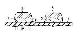
Fig. 1 schematically shows pads of a solder-coated
printed circuit board according to the first embodiment
of the present invention. A plurality of pads 2 are
formed on a board body 1 of an insulator by means of,
for example, pattern etching of a copper foil. A solder
layer 3 of a thickness necessary for electronic parts lead
soldering is formed on each pad 2 in order to mount
parts on the printed circuit board. The term "pad" used
2DB3682
- 10 --
here is a general term for the electronic part-mounting
portion, which includes, for example, the through hole
to which the parts are mounted. The term "pad"
hereafter is used to mean the above.
To form the solder layer 3, a solder precipitating
composition disclosed in Published Unexamined Japanese
Patent Application No. 1-157796 described above is used.
That is, the solder layer 3 is formed by a substitution
reaction between a powder of a metal having the highest
ionization tendency among metals constituting the solder
layer and a salt formed by bonding the other metal
(having a lower ionization level than the above metal of
the powder) in the solder layer to an organic acid.
A powder of a metal having the largest ionization
tendency among metals constituting the solder layer and
a salt formed by bonding the other metal or metals in
the solder layer to an organic acid, e.g., a car-
boxylate, are mixed to form a paste. When the paste is
coated on the pad 2 and heated, a substitution reaction
takes place between the metal constituting the powder
and the metal ion in the salt depending on the dif-
ference in ionization tendency. A free metal from the
salt is precipitated in the form of a metal around the
powder particles to form an alloy of the the powder
metal and the metal in the salt. For example, when a
lead salt of an organic acid (e.g., a lead carboxylate,
such as lead rosinate or lead acetate) is used as the
-
- 11 - 2063682
salt of the organic acid and a tin powder is used as a
metal powder having a large ionization tendency, an
Sn-Pb solder alloy is precipitated on the pad 2 by the
precipitating reaction described above.
In this embodiment, the pad 2 is formed to satisfy
2H ~ W where H is the projecting height of the pad 2
from the surface of the board body 1 and W is the width
of the pad 2.
Then, the paste-like solder precipitating com-
position coated on and around the pad 2, which includes
the lead salt of the organic acid and the tin powder as
the major components is heated, and solder alloy par-
ticles are formed by the substitution reaction. When
the solder alloy particles settle out in the paste
toward the pad 2, a small amount of solder attaches to
the side surface of the pad 2, and most of the solder
attaches to the upper surface of the pad 2, thereby
coating the solder layer 3 to a large thickness.
If 2H > W, the amount of solder attached to the
side surface of the pad is increased, and the amount of
solder on the upper surface of the pad which is required
for soldering is decreased. If a solder having an amount
necessary for soldering is to be coated on the upper
surface of the pad for 2H > w, the coating amount of the
paste-like solder precipitating composition must be
increased, which is uneconomical. In addition, since the
amount of solder attached to the side surface of the pad
- 12 - 2063682
is also increased, bridging between pads is often caused.
The value of 2H is preferably as smaller than W as
possible. For this purpose, it is effective to coat an
insulator 4, for example, a solder resist, between the
adjacent pads 2, as shown in Fig. 2, thereby decreasing
the projecting height H.
The second embodiment of the present invention will
be described.
Fig. 3 is a plan view showing a solder-coated
printed circuit board according to the second embodiment
of the present invention. In this embodiment, a
multiple of pads are arranged on a board body 1 at a
pitch of 0.5 mm or less to form a pad array 5 (four pad
arrays in Fig. 3). A solder layer is formed on each pad
by a precipitating reaction as in the first embodiment
(not shown in Fig. 3).
In this embodiment, as shown in Fig. 3, the width
of each of pads 2A located at two ends of the pad array
5 is set larger than that of each of pads 2B located
between the pads 2A.
Then, when a paste-like solder precipitating com-
position is solid-coated on the pad array to precipitate
a solder on each pad, the amount of solder flowing to
the pads located at the two ends of the pad array from
the portion other than the pads is relatively decreased,
since area of the each pat at the ends increases. As a
result, the thickness of the solder layer precipitating
- 13 - 2063682
on the pads at the two ends and that on the intermediate
pads can be uniformed. If it were not so, the solder
layers formed on the pads 2A located at the two ends are
thicker than the solder layers formed on the intermediate
pads 2B, since the amount of solder flowing to the pads
2A from the portion other than the pads is larger than
that to the pads 2B. It is preferable that the width of
each of the pads 2A at the two ends is set to about 1.2
to 2 times that of each of the intermediate pads 2B.
The third embodiment of the present invention will
be described.
Fig. 4 schematically shows pad-formed portions of
a solder-coated printed circuit board according to the
third embodiment of the present invention. In this
embodiment, a multiple of pads 2 are arranged on a board
body 1 at a pitch of 0.5 mm or less. A solder layer 3
is formed on each pad 2 by a precipitating reaction as
in the first embodiment.
In this embodiment, as shown in Fig. 4, the pads 2
are formed to satisfy W > D where W is the width of each
pad 2 and D is the pad-to-pad distance.
When the pad-to-pad distance D is set small in this
manner, a solder is efficiently precipitated on each pad
2 from the paste-like solder precipitating composition
coated between the pads 2, so that a thick solder layer
can be formed. In addition, the amount of paste-like
solder precipitating composition not contributing to
-
- 14 - 2063682
precipitation of the solder is decreased, which is eco-
nomical.
Note that in any of the above embodiments, to set
the thickness of the solder layer uniform, it is pre-
ferable that a pad length is not excessively larger thannecessary. The reason for this is as follows. When the
pad length is increased, the variation in pad width
along the pad lengthwise direction is increased. As
a result, the variation in thickness of the solder layer
formed on the pad is also increased.
The fourth embodiment of the present invention will
be described.
When a surface mounting part is mounted on a printed
circuit board, a guide mark for confirmation of a correct
position by image recognition is formed on the circuit
board in order to align the position of the parts lead
to that of the circuit board pad. This guide mark is
conventionally provided on a side of a pad array (between
outer and inner sides of the pad array). When the above-
described solder precipitating composition, for example,a paste-like solder precipitating composition containing
a lead salt of an organic acid and a tin powder as the
major components, is coated on the pad array to form a
solder layer, the paste-like solder precipitating com-
position is solid-coated. Thus, if the guide mark is
located at the position described above, the solder layer
is precipitated on the guide mark as well, making it
- 15 - 2063682
difficult to confirm the guide mark before parts mounting.
In order to prevent this, it is preferable that a
guide mark 6 for parts mounting is formed outside an
outer side L of each pad array 5 consisting of a
multiple of pads arranged at a predetermined pitch, as
shown in Fig. 5, so that the paste-like solder precipi-
tating composition is not coated on the guide mark 6, or
the paste-like solder precipitating composition supplied
to the portion other than the guide mark 6 dose not pre-
cipitate on the guide mark 6.
Fig. 5 is based on Fig. 3 showing the second embo-
diment. It is clear that the second embodiment can also
be applied to other circuit boards of other embodiments.
The fifth embodiment of the present invention will
be described.
On a solder-coated printed circuit board in which a
solder layer having a thickness necessary for parts lead
soldering is formed on each pad, it is preferable that
an in-circuit testing pad 7 to be connected to parts
leads are provided spaced apart from and connected to
each pad 2, as shown in Fig. 6. With such an in-circuit
testing pad 7, when a non-cleaning type flux is coated
on the solder layer of the pad and a parts lead is
soldered, even if the insulating flux remains on the
soldered portion to block off power supply from the out-
side, the in-circuit test can be performed using the
testing pad 7.
- - 16 - 2063682
The sixth embodiment of the present invention will
be described.
Fig. 7 schematically shows pad-formed portions of a
solder-coated printed circuit board according to the
sixth embodiment of the present invention. In this
embodiment, a plurality of pads 2 are formed on a board
body 1 in the same manner as in the first embodiment. A
solder layer 3 of a thickness necessary for parts lead
soldering is formed on each pad 2 to mount a part on the
printed circuit board.
In this embodiment, a gold layer 8 is formed on the
solder layer 3. In this case, the gold layer 8 can be
appropriately formed by a plating technique such as
electroless plating, or by a thin film formation tech-
nique such as sputtering.
In this embodiment, the solder layer is formed by aconventional method, for example, a method of printing
and heating a solder paste, a wave soldering method, a
hot air leveller method, and a method of performing
electroplating and heating. If the pad array pitch is
less than 0.5 mm, especially 0.3 mm or less, the solder
layer is preferably formed by the above-described
method, that is, a method of precipitating a solder
alloy by a substitution reaction between a metal salt
of an organic acid (for example, a lead salt of an orga-
nic acid) having a small ionization tendency and a metal
powder (for example, a tin powder) having the largest
- 17 - 2063682
ionization tendency constituting the solder alloy.
When the gold layer 8 is formed on the solder layer
3 in this manner, oxidation of the solder layer 3 can be
prevented. In addition, when a parts lead is placed on
the gold layer 8 and heated, gold is diffused in the Sn
or Sn-Pb plating on the surface of the parts lead, so
that sufficient wettability can be obtained for the
solder and the parts lead without using a flux. Also, a
printed circuit board with a solder layer having a gold
layer on it can be stored over a long period of time
before parts mounting. A cleaning step can be omitted
because a flux is not used.
In any of the embodiments described above, the
solder alloy constituting the solder layer is not par-
ticularly limited, and any solder alloy which is normallyused for electronic parts mounting can be used. For
example, in addition to the ordinary Sn-Pb type solder,
a low-melting solder containing Bi, In, Sn-Bi alloy or
Sn-In alloy can be used. In these case, a Bi, In, Sn-Bi
alloy or Sn-In alloy powder can be used as a powder of
metal or alloy contributing to the substitution reaction.
Example 1
A printed circuit board having a copper pad array
for mounting 0.3 mm-pitch QFP-type 160-pin parts was
fabricated. A projecting height H of each pad from the
surface of an insulating board was set to S0 ~m, a width
W of each of the intermediate pads (other than the parts
- 18 - 2063682
at the two ends) of the pad array was set to 150 ~m
(2H/W = 0.67), and the width of each of the pads at the
two ends was set to 200 ~m. A paste-like solder preci-
pitating composition containing lead salt of an organic
acid and a tin powder as the major components was coated
on the copper pad array to a thickness of 200 ~m and
heated at 215C for 2 minutes. Thereafter, the
remainder was cleaned off with trichloroethane. When
the thickness of the solder layer on the pads was
measured, it was 30 ~m on both the pads at the two ends
and the intermediate pads. Thereafter, an RMA-based
flux was coated on the solder layer and the QFP-type
parts described above were mounted. The whole structure
was heated to perform soldering. As a result, no defect
such as bridging or lead floating occurred at all.
Example 2
A printed circuit board having a copper pad array
for mounting 0.15 mm-pitch TAB-type 250-pin parts was
fabricated. A projecting height H of each pad from the
surface of an insulating board was set to 18 ~m, and a
width W was set to 90 ~m (2H/W = 0.4, D/W = 0.67). A
paste-like solder precipitating composition containing
lead salt of an organic acid and a tin powder as the
major components was coated on the copper pad array to a
thickness of 100 ~m. When the whole structure was pro-
cessed as in Example 1, a solder layer having a
thickness of 15 ~m was formed on each pad. Thereafter,
19- 2063682
the leads of the TAB parts were placed on the solder
layers and heat-pressed by a heating jig to perform gang
bonding. No defect such as bridging occurred.
Comparative Example l
A solder layer was formed by following the same
procedures as in Example l except that the width of each
of the two pads at two ends of the copper array was set
to the same as that (W = 150 ~m) of each intermediate
pad. As a result, the thickness of the solder layer was
60 ~m on the pads at the two ends and 30 ~m on the
intermediate pads. When a part as in Example l was
mounted, an open defect occurred in which some leads and
pads were not soldered.
Comparative Example 2
A printed circuit board having a copper pad pro-
jecting height H of 38 ~m and a width W of 60 ~m
(2H/W = 1.3) was fabricated and processed following the
same procedures as in Example 2. The thickness of the
solder layer on each pad was only 4 ~m. When parts were
mounted on this printed circuit board and soldered,
soldering failure of some of leads and pads occurred.
Example 3
A printed circuit board having a copper pad array
of a pitch of 0.3 mm was fabricated. A paste-like
solder precipitating composition containing a lead salt
of an organic acid and a tin powder as the major com-
ponents was coated on the copper pad array to
2063682
- 20 -
a thickness of 200 ~m, and the whole structure was heated
at 215C for 2 minutes, thereby forming a solder layer
to a thickness of 30 ~m on each pad.
Subsequently, fats and oils in the surface of the
solder layer were removed by a degreasing step, and the
solder-coated printed circuit board was dipped in a gold
electroless plating liquid of 80 to 90C for about 5
minutes, thereby forming a gold plating layer of a
thickness of 0.5 to 0.8 ~m on the surface of the solder
layer.
Then, the whole structure was washed with water and
dried sufficiently. Parts leads each having an Sn-Pb
plating layer were urged against the pads each having
the gold plating layer, with a heating jig. The heating
temperature was 280C, and the heating time was 3 to 5
seconds. No flux was used.
As a result, all leads were soldered to the pads
with good wettability with the solder. No bridging
occurred between the pads.
In order to check the long-term shelf stability, a
solder-coated printed circuit board of Example 3 on
which a gold plating layer was formed was washed with
water and left for 1,000 hours in a thermo-hygrostat of
40C and 95% RH. Thereafter, the circuit board was suf-
ficiently dried, and parts leads were soldered by
following the same procedures as in Example 3. In this
case, in the same manner as in Example 3, all the leads
` - 21 - 2063682
were soldered to the pads with good wettability with the
solder. No bridging occurred between the pads.