Note: Descriptions are shown in the official language in which they were submitted.
WO90/15997 PCT/US90/03059
206~213
MICRO-~AC~ L) ACCELEROMETER ~TT~
TILT COMPENSATION
This ~pplication is r~lated to Canadian
applicatlon serial number 603,258 filed June 19,
1989.
BACKGROUND OF T~E INVENTION
Field of the Invention
This invention relates generallv to
transducers which may be fabricated from
semi-conductor material such as silicon bv batch
photolithographic techniques~ from a
monocrvstalline wafer. More particularlY, the
invention relates to a sPring-mass-support
structure for detecting a signal proportional to
acceleration applied to the support structure.
The invention also relates to electronic circuitr~
in combination with the structure for detectinq
dis~lacement of the s~rinq suPported mass to
WO90/15997 PCT/US90/03059
2~6~213
produce analog or binary representations of
acceleration applied to the support structure.
Description of the Prior Art
A publication bv Kurt E. Petersen entitled
"Silicon as a Mechanical Material" published in
Vol. 70, No. 5 (May, 198?~ of the Proceedings of
the IEEE, survevs the art Oc micro-machining of
silicon to fabricate a mechanical device. The
Petersen publication describes etching techniques
commonlv used in fabricating micromechanical
devices and describes several devices which have
been made using such techniques. The publication
also describes a cantilever beam light modulator
array the beams Oc which are fabricated of silicon
dioxide. Another survey article appeared in the
April, 1983 publication of Scientific American
entitled, Silicon Micromechanical Devices by
Angell, et al.
An accelerometer having a micromachined
cantilever beam intended for in vivo biomedial
studies and which includes a piezoresistive
sensing element is described in a publication
entitled, "~ Batch-Fabricated Silicon
Accelerometer" by Roylance and Angell in IEEE
~ransactions on Electxon Devices,- Vol. ED-26, No.
12, December, 19?9.
U.S. patent Re.31,459 (reissue of U.S. Patent
~o. 4,071,838) reissued December 6, 1983 in the
name of Barr~ Block discloses a silicon folded
leaf spring force transducer fabricated by batch
photolithographic and etching techniques. One
embodiment of such transducer consists of four
WO90/~5~7 PCT/US90/03059
_
2064213
E-sprinqs located at 90 anqles about the central
axis of sensitivity. Piezoresistors disposed on
legs of the E-springs provide a measure of the
displacement of the springs in response to a force
applied to the transducer.
U.S. patent 4,155,516 issued March 13, 1979,
in the name of Harry Aine discloses first and
second leaf spring structures, as supported from
support structures, which are coupled together in
axially spaced mutually opposed relation
lC so that the first and second leaf spring
structures are coupled together for deflection in
unison relative to the surrounding support
structures in response to deflection of either of
the first and second spring structures. A
capacitive detector structure is provided for
detecting displacement of the leaf spring.
U.S. patent 4,597,003 issued June 24, 1986,
in the names of Aine and ~lock discloses a method
of chemical etching a silicon wafer by
undercuttinq an etch stopPed laver to fabricate a
cantilever beam supported at one end b~ a frame
structure with an integral mass formed by the
etch. Etching from opposite etch stopped lavers
of a silicon wafer is described. ~
While the art described above has advanced
the art of micro-machining of silicon wafers to
fabricate sensors in general and accelerometers in
particular, there remains a need for a
micro-machined structure of silicon and other
materials and associated electronics meeting
extremely precise specifications. For examPle,
_ ~ 4 ~ 2 0 6 4 21 3
extremely low distortion for an accelerometer is
required for certain applications. Prior art
spring configurations and materials are believed
to produce spring constants which change
unacceptably over a deflection range of interest.
Very low sensitivity to accelerations orthogonal
to the sensitivity axis is desired. Prior art
spring mass configurations do not provide
sufficient insensitivity to orthogonal
acceleration and angular motion applied to such
configurations. Very high dynamic range
(requiring extremely low noise) is desired in an
accelerometer which has not been provided by prior
art accelerometers and associated detecting
lS electronics systems. Shock impact insensitivity
is required in an accelerometer intended for use
in certain applications such as in the seismic,
automotive, or aeronautics fields.
SUMMARY OF THE INVENTION
Accordingly, primarily the invention seeks
to provide a micro-machined spring-mass sensor
which has springs having spring constants which
can be precisely controlled during the fabrication
process.
Further, the invention seeks to provide a
geometry of a spring-mass-support transducing
element which results in an accelerometer which
has very low distortion and has a very low
sensitivity to motion orthogonal to its
sensitivity axis and to angular motion.
Still further, the invention seeks to
provide an accelerometer sensor which when
subjected to extremely high shock impacts will
survive undamaged.
20642 1 3
- 4a -
Further still, the invention seeks to
provide a micro-machined sensing device and
associated electronics resulting in an
accelerometer with an extremely broad dynamic
range.
Still further, the invention seeks to
provide a batch fabricated micro-machined sensing
element with associated electronics for producing
a signal representative of acceleration applied
along the sensitivity axis of the element.
The invention also seeks to provide a batch
fabricated micro-machined sensing element with
associated electronics to produce a binary bit
stream representation of acceleration applied
along the sensitivity axis of the element.
Still further, the invention seeks to
provide a batch fabricated micro-machined sensing
element with associated electronics by which
accelerations of low frequency and high frequency
may be determined in separate feedback loops
effectively allowing large slowly varying
accelerations to be measured simultaneously with
smaller higher frequency accelerations thereby
decreasing dynamic range requirements of the
sensor in the measurement of such higher frequency
accelerations.
20~421 ~
- 4b -
The invention in one broad aspect provides a
transducer comprising sensing means for generating
a displacement signal of a mass from a reference
position with respect to a support structure, and
first forward circuit means including high pass
filter means responsive to the displacement signal
for creating a high-pass filtered displacement
signal and converting same to an output binary bit
stream representative of the high-pass filtered
displacement signal. Second forward circuit means
includes low pass filter means responsive to the
displacement signal for creating a low pass
filtered displacement signal, and converts same to
an output low frequency signal representative of
the low pass filtered displacement signal. First
feedback circuit means is responsive to the output
binary bit stream for generating a binary force on
the mass in a direction tending to restore the
mass to the reference position, and second
feedback circuit means is responsive to the output
low frequency signal for generating a low
frequency force on the mass in a direction tending
to restore the mass to the reference position.
Thus, the output binary bit stream is
representative of a characteristic of motion of
the support structure at frequencies passed by the
high pass filter, and the output low frequency
signal is representative of a characteristic of
motion of the support structure at frequencies
passed by the low pass filter.
206421 3
- 4c -
The invention also comprehends a system for
detecting the direction of acceleration forces of
sound waves in a body of water comprising a
submerged platform supported via a cable from a
floating buoy, the platform characterized by an x
axis and a y axis, each perpendicular to each
other and perpendicular to the cable, the cable
defining a Z axis which may be tilted from true
gravitational axis of the earth by wave and
current action on the buoy and said platform. A
first accelerometer is mounted on the platform
such that its axis of sensitivity is coexistent
with the x axis of the platform, and a second
accelerometer is mounted on the platform such that
its axis of sensitivity is coexistent with said y
axis and of the platform. Each of the first and
second accelerometers have sensing means for
generating a displacement signal of a mass from a
reference position with respect to a support
structure, means responsive to the displacement
signal and including a high pass filter for
generating a detection signal representative of
acceleration of the support structure at
frequencies passed by the high pass filter, and
means responsive to the displacement signal and
including a low pass filter for generating a low
frequency gravitational signal representative of
acceleration of said support structure at
frequencies passed by said low pass filter. Means
responsive to the low frequency gravitational
~ 5 - 20642 1 3
signal is generated by the first accelerometer for
determining the angle of tilt ~ of the platform
with respect to the true gravitational axis of the
earth with respect to the platform x axis, and
means responsive to the low frequency
gravitational signal is generated by the second
accelerometer for determining the angle of tilt
of the platform with respect to the true
gravitational axis of the earth with respect to
the platform y axis. Means responsive to the
angle of tilt ~ x and the detection signal of the
first accelerometer translate the detection signal
along the x axis of the platform in the absence of
tilt, and means responsive to the angle of tilt
0 y and the detection signal of the second
accelerometer translate the detection signal along
the y axis of the platform in the absence of tilt.
More particularly, the aspects
identified above as well as other
features and advantages of the invention
are incorporated in a device including a
WO90/15997 PCT/US90/03059
-6- 20~4213
mass-spring-support sensin~ structure and
associated electronics. The sensing structure
includes a micro-machined transducer having a
support frame and a sensing mass supported from
the frame by at least one, preferablv eight,
E-shaped leaf springs. Each of the eight
E-springs have a base with two outer legs and an
inner leg. Each leg is connected to the base at
one of its ends. The two outer legs connect to
the frame at their other ends. The inner leg is
connected to the mass at its other end. The base
is characterized bv a coefficient of stiffness
substantially greater than that of the legs. Each
of the legs are preferablv the same length. Tn
order to preciselv define the spring constant o r
the sprinqs, the legs are fabricated of silicon
dioxide, because the thickness of the silicon
dioxide springs mav be preciselv controlled during
the fabrication process.
The mass-spring-support sensing structure is
fabricated by orienting four E-shaped leaf spring
structure patterns on top and bottom (lO0) faces
of a silicon wafer such that they are oriented at
forty-five degree angles with respect to
intersection lines of ~111) planes of the wafer
and the opposite faces of the wafer. The opposite
faces are masked and silicon dioxide grown on
surfaces which will ultimately be etched awav bY
an etching chemical. A thin layer which is a stop
laver is formed. This laver can be formed bY
diffusing into this laver an impuritv, such as
arsenic, that will change the semiconductor tvpe
2064213
from P to N in this layer for an impurity such as
arsenic which will form a P/N junction between the
laver and the substrate. A voltage bias can then
be applied to this layer to form an
electromechanical etch stop layer. The arsenic is
diffused into opposite surfaces of the wafer
everywhere except the "opening" surfaces and the
surfaces which will ultimatelv serve as the legs
of the spring.
A thick oxide layer is then grown bv
diffusing a precise amount of oxvgen into the
silicon to form a precise thickness of silicon
dioxide on the silicon wafer. Next, the opposite
surfaces of the wafer are masked exposing onlY the
regions which will not be the springs of the
structure as well as some other selected areas.
These exposed areas of silicon dioxide are then
etched down to the silicon surfaces. A thin
silicon dioxide la~er is then grown, masked, and
the exposed silicon dioxide etched down to the
silicon surface in the regions that will be
exposed to the silicon etchant. Chemical etch of
the silicon material then is applied which acts
through the openings of the silicon dioxide to
etch silicon material away while~ undercutting the
springs, leaving a central mass supported bv
silicon dioxide spring legs. Stiff etched-stop
lavers remain for the bases of the springs and the
opposite faces of the suspended mass and support
structures.
,o Force and sense conducting areas are then
deposited on opposite faces of the suspended mass.
-8- 20S~213
Conductors are deposited which run from the
conducting areas via spring legs to the support
structure. First and second plates havinq
corresponding force and sense plates with
conductors running to external connecting pads are
fixed to opposite support surfaces of the
mass-spring-support structure such that each of
the conducting surfaces of the mass ~reciselv face
a corresponding conducting surface of the first
and second plates.
An electrostatic electronic feedback svstem
is provided to detect displacement of the mass of
the mass-spring-support structure in response to
acceleration or force applied to the support. For
frequencies of the applied acceleration below the
resonant frequencv of the mass-spring-support
structure, displacement of the mass is
proportional to acceleration. Displacement of the
mass (and consequentlv the acceleration~ applied
to the support structure is measured by applvinq a
first voltage between the sense conducting areas
o~ the opposite plates and applying a second
voltage between the force conducting areas of the
opposite plates. The first voltage creates a
sense electric field between the-sense conducting
2~ areas of the suspended mass and induces a sense
voltage on it proportional to the displacement of
the mass between the opposite plates. The second
voltage creates a force electric field between the
force conducting areas of the mass.
A forward circuit responsive to the sense
voltage generates a displacement signal which is
2~21~
representative of the displacement that the mass
has moved from a reference position between the
plates. A feedback circuit responsive to the
displacement signal applies an amount of electric
charge on the force conducting area of the mass
surface such that a force is created on the mass
proportional to the product of the amount of
charge and the force electric field so as to
substantiall,v restore the mass to the reference
position. The displacement signal is an analog
representation of acceleration. The first and
second voltages mav be d.c. voltages, or may be
square waves operating at a modulation frequencv
higher than expected frequencies of the
acceleration to be measured. A demodulator is
required to produce an unmodulated analoq output
signal representative of acceleration.
Another embodiment of the invention, like the
ones described above, includes a sensor for
generatin~ a displacement signal representative of
displacement of a mass from a reference position
with respect to a support structure. A forward
circuit i-s provided which, in response to the
displacement signal, converts the displacement
signal to an output binarv stream. A eedback
2; circuit, in response to such output binar,v stream,
generates a binarv force on the mass in a
direction tending to restore the mass to the
reference position. ConsequentlY, the output
binarv stream is representative of a
characteristic of motion, preferablv acceleration,
of the support structure.
2U6421 3
--1 o
An alternative embodiment of the sensor and
accelerometer is provided for an application where
the accelerometer is placed on a platform subiect
to tilt. Tilt of such platform causes a
potentiallv large slowly varying gravitational
acceleration to be coaxial with small higher
frequencv accelerations desired to be measured.
The sensor is provided with additional "gimbal
force" plates in addition to the force plates of
the sensor described above. Separate electronic
feedback circuits, one including a low pass
filter, the other including a high pass filter,
are provided bv which a displacement signal of the
mass of the sprinq-mass-support system is sensed
and fed back in two paths to null the mass in the
1~ ace of accelerations applied to the support.
In one arrangement, a low frequencv analog
signal is applied to mass gimbal force plates
while a constant charge is applied to opposing
corresponding support plates. A high freq,uency
binarv bit stream signal is applied to mass force
plates while a constant charge is applied to
opposing corresponding support plates. The low
frequency analog signal is representative of
tilt-induced gravitational acceleration. The high
frequencv binary bit stream is ~epresentative of
the higher frequencv acceleration of a signal the
detection of which is sought.
In another arrangement, the low frequencv
analoq signal is a~plied to mass gimbal force
plates while a constant charge is applied to
opposing corresponding su~port plates. A high
20642 1 3
frequenc~ binary bit stream is applieA to a char~e
generator to produce a corresponding charge signal
which is applied to mass force plates. A constant
voltage is applied across opposing corres~onding
support plates.
Apparatus is also provided for translating
the high frequencv signal representation of
acceleration to an untilted orientation bv using
the low frequencv representation of tilt-indu~ed
gravitational acceleration.
~RI~F D~SCRIPTIO~ OF THE DRAWINGS
The objects, advantages and features of the
invention will become more apparent bv reference
to the drawings which are appended hereto and
wherein like numerals indicate like parts and
wherein an illustrative embodiment of the
invention is shown, of which:
Figure 1 is a transverse sectional view of a
wafer of monocrvstalline material from which a
spring mass svstem is to be fabricated according
to micro-machining techniques of the invention;
Figure 2 is a view similar to that of Figure
1 showing an oxide layer formed on opposite sides
of the wafer;
Figure 3 is a plan view of the wafer of
Figure ~ showin~ areas for which
spring-mass-structures will be fabricated;
, .
206421 3
Figure 4A is an enlarged view of an area of
Figure 3 as indicated by line 4A of Figure 3 which
indicates the orientation of the crystal top and
bottom surfaces and its relation to (111) planes
of the crystal;
Fiqure 4R is a sectional view o_ the wafer
showing a part of the lavout taken along the lines
4~-4B of Figure 4.~ with photo-resist material
having been applied to the opposite sides of the
wafer;
Figures 5A and ~ are simllar to Figures 4A
and 4B but show a wafer portion after it has been
masked with a pattern of a spring-mass-support
structure, and after portions of the oxide lavers
have been removed, leaving a pattern of oxide
partiallv defining ultimate etching openings on
the opposite sides of the wafer;
Figures 6A and 6B are similar to Figures 5A
and 5B but reflect further processing after etch
stop material has been diffused into the crystal
of the wafer on opposite surfaces in areas other
than the etching openings and spring legs;
Fi~ures 7A and 7B are similar to Figures 6A
and 6~ but reflect further processinq after
opposite wafer surfaces have been~masked to allow
further etch stop laver mate~ial onto wafer
surfaces where surrounding support structure,
central mass and bases of E-springs are patterned;
Figures 8A and 8B are similar to Figures 7A
and 7B but reflect further processing after the
etching openings on both sides of the wafer have
had oxide previouslv covering them removed and
`-- 20642 1 3
show a relatively thick laver of silicon dioxide
material having been grown ov~r areas of the sides
of the wafer defining E-spring legs;
Figure 9A shows a plan view of the one-half
of the wafer after chemical etching of the wafer
through etch openings has etched to (111) planes
of the crystal of the wafer thereby undercutting
the E-spring structure.s and severing the mass
portion of the structure from the support portion
while suspending the mass from the support and
after further processing where the thin laver of
etch stop material beneath oxide sides of the
springs have been removed;
Figure 9B is a sectional view of the wafer
illustrated in Figure 9A taken along section lines
93-9~;
Figure 10 is a p~rspective view of the
sensing element structure including support,
~-springs and sensinq mass, the view being
partially cut-awav to illustrate the central mass
severed from the support structure to show the
oxide springs and undercut etch stop layers of the
mass, springs and support structure;
Figure 11 illustrates a cross-section through
the sensing element showing t-he sensing mass
supported bv springs to undercut portions of the
support member where gravit~ forces the mass to be
disposed beneath the top plane of the support
member, the view further showing a composite
structure including top and bottom plates having
force and sense conductinq areas deposited on
their faces corresPonding to similar force and
2064213
sense conducting areas on opposite surfaces of the
sensing mass;
Figure 1' is a plan view of the sensing
structure illustrating deposited conducting leads
to the force and sense conducting areas of the
5 mass surface from the support structure via the
E-spring leads;
Figure 13 is a schematic illustration of an
electrostatic feedback control system for
detecting acceleration applied to the support
system by substantially maintaining the sensing
mass at a predetermined position between the
opposite plates of the composite structure, the
output of the system being an analog signal
proportional to applied acceleration;
Figure 14 shows a schematic illustration of a
svstem similar to that of Figure 13 but having an
alternating voltage applied to the covering plate
force and sense conducting areas, with a
demodulator provided to develop an analog signal
proportional to applied acceleration;
Figure 15 is a schematic illustration of a
charge generator circuit used directlv or with
modification in the transducer sYstems of ~igures
13, 14 and 16, 17, 18 and 19;
2~ Figure 16 is a schematic illustration of a
transducer having a binary bit stream output
representative of the displacement or acceleration
of a mass in a mass-spring-support structure with
binary bit stream volta~es applied to top and
bottom force plates and with a constant charge
applied to force plates of the mass with the
WO ~/15~7PC~r~9~
20642 1 3
.
--15--
result tha~ a binar~ force is app~ied to the mass
tending to restore ~t to its reference position;
Figure 16A is an illustration of a binary
sampler used in the embodiments of Figures 16, 17,
18 2na 19;
Figure 17 is similar to the transducer of
Figure 16 except that a binary ~ stream of
char~e is applied to the force pla~es of the mass
and a constant elec~ric field is applied across
the force plates of the top and bottom plates;
Figure 18 is similar to ~he transducer of
Figure 17 except that an electric field applied to
the force plates of the top and ~o~tom plates is
modulated with an a.c. signal, and consequently
the binary ~it stream of charg~ applied t,o the
t5 forçe plates of the mass is al50 modulated;
~igure 19 is similar to the transducer of
-Figure 18 except that the charge applied to the
force plates of the mass is modutated and
modulated bit streams of the output signal are fed
back to the force pla~es of the top and bottom
plates;
~i~ures 20A-20C illustrate an application of
the transducer o~ the invention used ~o measure
' acceleration on a su~merged platform sub~ect to
tilt caused ~ wa~e and current act~on of the
water;
Figure 21 is a plan view o the mass ~nd
spring me~ers of the sensing element of ~he
transdu~er modified to include a gimbal force
plate on the mass
~ U~ ~77 ~
20~13
-16-
Figure 22 is a vertical cross-section through
the sensing element illustrating sense, force, and
gimbal force conducting areas on the mass and
corresponding conducting areas on plates attached
to a supporting member and which face the
conducting areas on the mass;
Figure 23 is a schematic diagram of an
accelerometer showinq two feedback loops for
maintaining the mass of the sensing element at a
position between opposing facing plates above and
below the mass, where a low frequenc~ loop is
responsive to slowly varying gravitational
acceleration due to the tilt of a platform on
which the sensor is placed and a high freauencv
loop is responsive to high frequency
accelerations;
Figure 24 is a schematic diagram of an
accelerometer similar to that of Figure 23 but
with an alternative technique for applving
electrostatic feedbac~ forces to the mass;
Figures 25A and 25B are schematic diagrams
showing the frequency characteristics of a low
pass filter and a high pass filter used in the
embodiments of the accelerometers of Figures 23
and 24; and
Figure 26 is a block diagram of a digital
computer used in coniunction with x and y
accelerometers mounted on a submerged platform,
such diagram illustrating computations for
correcting measured accelerations for the effect
of tilt of the platform in the water.
- 20642 1 3
DESCRIPTION OF THE INtlENTION
Two important motivating factors, among
others, led to the accelerometer of this
invention. The first is low manufacturing cost so
that the resulting accelerometer may find wide
5 application where manv force sensing transducers
are required. The second is an accelerometer
having extremely high performance characteristics:
wide dvnamic range; low distortion; low
sensitivitv to motion orthogonal its sensitivitv
axis; and resistance to high shock impact. These
requirements lead to the fabrication of the
accelerometer bv micro-machining techniques from a
monocrystalline material such as silicon.
Referring now to Figure 1, a typical wafer 10
is shown from which a batch of accelerometers are
to be fabricated according to the process of the
invention. In a tvpical example, the wafer 10 is
made of a nonmetallic monocrvstalline material
such as silicon, germanium, quartz, gallium
arsenide, gallium phosphide, etc. In a preferred
embodiment, the wafer 10 is made of a diamond
cubic material, such as silicon. The wafer 10 has
a thickness of about S00 microns, has polished top
and bottom surfaces 12, 14 and has a convenient
diameter, such as 3 to 8 inches. In the case of
diamond cubic material, the crystallographic plane
(100) is preferablv formed at the upper 12 and
lower 14 maior surfaces of the wafer 10.
Furthermore, the wafer 10, in the case of silicon,
is preferablv doped with a P tvpe dopant to a
conductivitv of between 0.1 - 10.0 ohm-cm.
- 20642 1 3
-18-
In the next step of the process, the wafer 10
is oxidized on opposite sides to form oxidized
lavers 16, 18 of 2500 angstroms in thickness as
illustrated in Figure 2. This is convenientlv
achieved by putting the wafers in a furnace at
1100 C, in the presence of oxygen. NeY.t, the
oxide lavers 16, 18 are each coated with a
photoresist material such as KMER.
Figure 3 is a plan view of the wafer with
multiple areas each of which are to be processed
simultaneously to batch produce the
mass-spring-support structures of the invention.
One particular area is illustrated in Figure 3
with line 4A-4A, shown much enlarged in Figure 4A.
The boundary edges 24 of the structure to be
fabricated are oriented parallel to the (111)
planes o the crystal as illustrated in Fiqure 4A.
Each structure o~ the array of structures of
Figure 3 will ultimately be cut along the boundarv
edqes 24 parallel to the (111) planes of the
crvstal after batch processing. Figure 4B shows a
cross-section through a portion of the wafer
showing the RMER photoresist laYers 20, 22
deposited over silicon dioxide layers 16, 18.
Figure SA shows one side of the wafer (for
convenience called here the top side) after
masking and exposure of the pattern as depicted
thereon. The unexposed photoresist portion covers
the etch opening patterns 30' and the spring legs
30'', but the remainder of the photoresist
portions are removed by exposure and development
of the photoresist. The wafer is then placed in a
- 20642 1 3
--19--
silicon oxide etch solution such as buffere~
hvdrofluoric acid, which attacks the oxide but not
the photoresist or the underlying silicon. The
photoresist protects the pattern 30 as illustrated
in Figure 5A. The pattern 30 includes two parts:
5 the regions indicated bv 30' will ultimately be
etch openings; the regions marked 30'' will
ultimately be spring legs. Figure 5B shows a
cross-section through lines SB-5B of Figure 5A and
illustrates the oxide portions 30' and 30'' on top
and bottom surfaces 12, 14 which respectivel~
ultimately form a slot opening behind the base of
the E-spring and the middle leg of the E-spring.
Oxide portions 30' and 30'' are greatlv enlarged
in Figure 5B for ease of illustration.
lS The oxide pattern 30' of Figures 5A and 5B
will ultimately ser~e as the etch openings to
fabricate the three dimensional
mass-sprinq-support structure of the
accelerometer. The oxide patterns of 30'' will
ultimatelv be the location of the spring legs of
the E-springs. A perspective view of the
structure mav be seen in cut-awav sectional view
of Figure 10 showing the structure at a certain
stage in the processing.
Figure 5A illustrates particular features of
the grown oxide patterns 30' and 30'' which
ultimately will result in the structure of Figure
10. The lines 32-32 of Figure 5B show a region in
which an "E"-shaped spring 40 will be fabricated
to partiallv support a mass 36 from a surrounding
support structure 38. The E-spring 40 will
206~2 1 3
-20-
include a base 42 and three legs 44, 46, 48.
Slots or openings 43, 45, 47 will ultimately
outline the shape of the E-spring. The inner leg
46 is twice the width of outer legs 44, 48. The
lengths of the legs 44, 46, 48 are preciselv the
5 same.
Each E-shaped spring 40 is placed at the
corner of intersecting (111) planes, that is, at
45 angles to intersecting lines of (111) planes
which intersect the surfaces 12, 14 of the
mono-crystalline wafer 10. The base 42 of each
spring will ultimately be fabricated of stiff etch
stop material while each leg 44, 46, 48 will
ultimatelv be fabricated of silicon dioxide, as
described below in more detail.
Two characteristics of the shape of the
pattern of lines 32-32 are important. ~he first
relates to the area identified bv arrow 50, which
connects the inner leg 46 to the sensing mass 36.
Solely for purposes of illustration and
description, this region is called the "cat head
with ears" region, and is pointed to by reference
arrow 50. The top of the cat head is attached to
inner leg 46 with its "neck" or "body" attached to
mass region 36. The "ears" of the cat head and
2~ ears region extend into oxi~e areas which
ultimatelv will be openings between sensing mass
region 36 and support region 38. The cat head and
ears geometry provides a stiff region of mass 36,
ultimately to be fabricated of undercut etch-stop
material, to which inner leg 46 is connected.
2Q~21~
-21-
The second shape relates to an area pointed
to by reference arrow 52 of Figure 5A. Solely for
purposes of illustration and designation, this
region is called the "hockev stick" re~ion because
of its general resemblance to the shape of a
hockev stick. This hockey stick region,
ultimatelv to be undercut etch stopped material
between regions 43 and 56 (which ultimatelv will
be openings formed by means of silicon etching~,
provides a relativelY wide region at the top of
the foot of the hockey stick by which outer leg 44
(or 48) attaches to etch stopped material. Such
wide region provides a strong connection between
the ends of the outer legs of the E-springs and
the etch stopped material of the surrounding
su~port structure.
The oxide areas 56 (which ultimately will be
openings) have edges 58, 60 which are coexistent
with intersecting lines of (111) planes of the
crystal with the (100) surface 1~ of the wafer.
These areas 56 serve as "etch-time and undercut
control" areas and are given the short-hand
notation, "ETUC" areas. They ultimatelv serve as
large open areas bv which etchant chemical will
undercut E-springs 40. Their~ area must be
relativel~ large to allow et~hant to etch to
intersect (111) planes having intersecting lines
62, 64 with the surface 12. Areas 56 must be
large enough to speed the etching process to
completion to the intersection of the planes of
the intersecting lines 62, 64, but must be shaped
as shown to provi~e the "hockev stick" etch
20642 1 3
-22-
stopped areas 52 on its sides as discussed above.
The inner edge 60 defines the intersecting line of
a (111) plane of the crystal which will define the
outer surfaces of the mass region 36.
Another factor dictating the shape of ETUC
areas 56 is the requirement that during chemical
etching, the mass region 36 must be severed from
the surrounding support frame 38. Chemical
etching of the silicon wafer occurs in one
direction along (111) planes which intersect with
lines such as 64 and 62 of the top and bottom
surfaces which are extensions of edges 58 of ETUC
areas. Chemical etching of the silicon wafer
occurs in the opposite direction along (111)
planes which intersect lines which e~tend from
inner edges 60 of the ETUC areas of the top and
bottom surfaces. When the etching rrom the
opposite directions along (111) planes meet, the
mass 36 is separated from support frame 38 as can
be seen in Figure 9~. Consequentlv, the distance
between edges 58 and 60 must be great enough to
allow the mass region 36 to be separated from
support frame 35 during chemical etching.
Turning now to Figure 6A, the silicon dioxide
regions 30' defining openings of Figure 5A and the
spring leg regions 30'' are ~masked, and the
uncovered silicon portions are implanted with a
thin layer of arsenic. The arsenic is diffused a
short distance, (6 to 7 microns) in the silicon to
form N layers on top and bottom surfaces that are
used as electrochemical etch stop layers in the
silicon crystal. This stage of the processing is
- 2~642 1 3
-23-
illustrated in the cross-section of Figure 6B.
Next, the oxide of spring leg region 30'' (of legs
44, 46, 48) is removed and an additional two
micron thickness of arsenic is diffused into the
silicon. Figure 7B shows this stage of the
processing. The thickness of the etch stop layer
70' is now about 8-9 microns thick.
In preferred processing of the
mass-spring-support structure of this invention,
the thick la~er of arsenic is especiall~ importan~
to impart stif~ness to certain regions of the top
and ~ottom etch stop layers. The base of the
springs 42, cat head region ~ n and the hockey
stick region 52 require stiffness and strength to
connect with the spring legs 44, 46, 48 so that
1~ the mass region 36 mav be adequatelv supported
from support region 38.
Figures 8A and 8~ show the condition of the
wafer after the silicon dioxide regions 30' have
been stripped from the wafer 10, a thick layer
(1.2 microns) of silicon dioxide has been regrown
evervwhere over top and bottom surfaces r and
finallv such silicon dioxide has been stripped
awav everywhere except over spring leg portions
44, 46 and 48. Silicon dioxide lave_ 30'''
2; remains for such legs as is shown in Figure 8B.
At this point in the processing, conductive areas
are provided on the opposite faces of the mass
region 36 and conductive leads running from the
support region via the legs 48 or 44, 46 and base
42 are deposited. For simpli~ication of
illustration, the results of providing such
20~213
-24-
conductive region and leads are illustrated in
Figure 12 and described below.
Next, the wafer is subjected to
electro-chemical etching such that the wafer is
etched away from the ETUC areas 56 and other open
areas, such as slots 43. The etch chemical etches
beneath etch stop layer 70' preferentially along
(lll) planes o~ the crystal of the wafer. The
preferred etching process is similar to that
described in U.S. patent 4,597,003, described
above and incorporated herein bv reference for its
electro-chemical etching methods. Next, the thin
lavers 70''' (Figures 7B, 8~) of etch stop
material are removed by sub~ecting the wafer to a
silicon etch (either dip or plasma) evervwhere.
Such etching causes etch stop laver 10' to be
reduced in thic~ness bv about 2 microns, that is,
to an ultimate thickness of about 6-7 microns.
The result of the processing described above
is a three dimensional support-sprinq-mass
structure illustrated in plan and cross-section
views of Figures 9A and 9~ and the perspective
view partially broken awav of Figure 10. The
etching process has etched the silicon material
away, along the (lll) planes -defined bv the
intersection of such planes with ^lines parallel to
edges 58, 60 of each of the ETUC areas 56.
Undercut etch stop laYers 70' are visible in
Figures 9B and 10 as well as the suspended mass
36, surrounding support structure 38 and silicon
dioxide spring layers 30'''. The bases 4~ of the
2Q6~21~
WO ~oJ~sss7 Pcr/usso~030sg
-25-
E-~pring~ 40 are formed of undercut etch stop
material 70' as seen in Figure 9B and lO.
An important feature o the invention is
apparent from Figure~ 9A and 9B. That feature is
the fact that bases 42 of the E-springs are
S fabricated of etch stop material 1~' wh~le the
legs 44, 46, ~8 o~ the E-springs are substantially
entirely of si~icon dioxide. ~his difference in
materials allows the stiffness of the base of each
E-spring to be substantiallv greater than that of
the legs.
The coefficient of stiffness (Young's modlus)
is approximatelY th~ee times grea~er for silicon
than it is for sili~on dioxide. The thickness of
the base 42 a~ each E-spring is controlled ~uring
lS processing to be greater than seven times as thic~
as tha~ o~ the silicon dioxide legs. The
resulting stiffness of the base, consequently, is
seven cube~ times three, or more than lO00 times
stiffer than the le~s for similar leng~hs and
w~dths of material.
~ach spring leg 42, 46, 48 of each E-spring
is precisely the same length ~rom its
connection at one end of ~ts respecti~e base 42 to
its respective connection to either the ~op of the
foot of the hockey stick area or to the head of
the "cat head with ears" area. It is fabricated
of silicon dioxide, as described above, becau~e
the thicknes~ of the silicon dioxide legs may be
verv accuratelv controlled. The length of each
leg and its thickness must ~e accurate~
control1ed so as to control the spring constant o
20642 1 ~
-26-
the sensing member. It can be shown that the
spring constant of the E-spring is proportional to
the cube of the thickness of its legs. Another
reason for fabricating the legs of each E-spring
of silicon dioxide is that silicon dioxide is a
well-behaved material in that it has no measurable
hvsteresis and it does not fatigue over many
cycles of flexing.
- Legs 44 and 48 are precisely the same width.
Leg 46 is made up of one or more side bv side legs
whose composite width is precisel~ twice the width
of legs 44 or 48. Although not illustrated, leg
46 is preferably a composite of three side bv side
legs, each leg of course having a smaller width
than the composite width. Dividing the total
width of leg 46 into three parts has been found to
prevent buckling or crinkling of leg 46 after
processing.
Figure 11 shows a cross-section of sensing
element 80 sandwiched between opposite su~po_ting
members 82, 84. Sensing element 80 shows central
mass 36 supported via spring legs 46, 48 and legs
46, 44 via bases 42 from surrounding support
member 38. The mass 36 is shown displaced
vertically by the force of gravitY. The sense
2~ conducting areas 90 formed on opposite sides of
the faces of mass 36 surround force conducting
areas 92. Figure 12 shows a plan view o the
support-spring-mass structure 80 with the force
and sense conducting areas 92, 90 formed on the
top face of the mass 36. Such areas 90, 92 are
conductivelv isolated from each other. Although
WO~ 997 PCTJUS9~nn~
20u~2 1 3
-27-
not shown in Fi~ure 12 for simplification o
illustration, guard regions are provided between
area~ 90,9.~ to reduce the capacitive coupling
between ~uch areas. Corresponding force and sense
conducting areas 92', 90' are provided on plate
surfaces formed on opposite supporting members 82,
84. Such plate surfaces and force and sense
conducting areas 92', 90' correspond in size and
pattern ~o the opposite surface~ of mass 36 ~nd
its force and sense conducting areas 9~, 90.
Opposite supporting members are bonded to the
support member 38 ~y conventional means.
Figure 12 shows conductors running from
external connection pads ~o the force and sense
plates. Such conduc~ors are illustrated fo~ one
sur.face of the support-spring-mass structure 80 as
an illustration of such conductors provided to the
senQe and foxce conducting areas of ~he top and
bottom pl*tes 82, 8~ and the opposite surfaces of
mas~ 36. Conductors 94 and 96, preferablY gold,
~se deposited on opposite surfaces of the wafer
and structure 80 suc~ that the~ run respec~ivel~
from connecting pads 98 and 100 ~ia separate
E-sprin~s 40A and 4QB. As illustrated, lead 94
connects to f~rce conducting area 92 via leg~ 48
and 46 and ~ase 42 ~f ~-sprinq 40A, while lead 96
connects to sense conducting area 90 via legs 44
and 46 and base 4~ of E-spring 40B.
The leads 94 and 96 respecti~relY pass through
tunnels 102, 104 pr~ided for a seal (no~ shown)
~etween sandwiched surfaces of support member 3B
and opposite supporting members 82, 84. Conductor
wo yu/ ~
- 20642 1 3
-28-
94' is deposited on opposite leg 44 and a portion
of base 4~ of spring 40A to balance the weight and
stiffness of conductor 94 on leg 48 and base 42.
Likewise, conductor 96' is deposited on opposite
leg 48 and a portion of base 42 of spring 4OB to
balance the weight and stiffness of conductor 96
or leg 44 and base 42. Conductor 94' is not
electricall~ ccnnected to conductor 94. Likewise,
conductor 96' is not electrically connected to
conductor 96.
Conductors 106 and 108 are deposited on
E-springs 40C and 4OD, but have no external
electrical connection. Such conductors 106 and
108 provide weight and stiffness to springs 40D
and 40C to balance the weight and stiffness of
conductors deposited on springs 40A and 40B. F,ach
of the four surfaces, two opposite faces of mass
36 and opposing surfaces of opposite support
members 82 and 84, have similar conducting leads
attached to their respective force and sense
conducting areas. Such leads are connected to
appropriate pads illustrated ad~acent pads 98,100
of Figure 1~ which communicate with electronic
circuitrv described below.
Turning now to the electroni~c circuitrY
associated with the spring mass transducer
described above, three alternative embodiments of
transducer systems, or accelerometers, are
illustrated respectivelv in Figures 13, 14 and 15.
Figure 13 shows a mechanical schematic of the
spring mass transducer of Figure 11.
~ UI I J.7 ~ ~
`- 206421 3
-29-
Mass 36 is supported from a support 38 via
springs 40 having substantially equal spring
constants of 2ks. A d.c. voltage of magnitude Vcc
is applied between sense conducting areas 90' on
plates of opposite support members 8~, 84, which
; of course are fixed with support 38. A d.c.
voltage of magnitude Vqq (which may be the same as
or different from magnitude Vcc) is applied
between force conducting areas 92'. Leads 96
connected to top and bottom sense conducting areas
90 of mass 36 are connected to lead 110. Leads 94
connected to top and bottom force conducting areas
92 of mass 36 are connected to lead 112.
A differential amplifier 120 has one of its
two inputs connected to lead 110 with another of
its leads connected to a reference voltage which
is provided with some fraction of magnitude Vcc,
preferably, one half vcc. The voltage appearing
on lead 110 is proportional to the position o~
mass element 36 between the plates Oc support
members 8~ and 84, because a sense electric field
is created between sense conducting plates 90' by
voltage Vcc, and because sense conducting plates
90 of mass 36 are disposed in the path of that
sense electric field. When the masa element 36
moves toward the plate of top suppo~t member 8~,
the voltage on sense plates 90 and lead 110
approach the magnitude Vcc; conversely, when the
mass element 36 moves toward the plate o~ bottom
support member 84, the voltage on sense plate 90
and lead 110 approaches zero or ground magnitude.
20642 1 -~
-30-
Consequently, with the reference voltage
Vcc/2 applied to differential amplifier 20, its
output on lead 122 is a sense displacement signal
proportional to the distance that mass element 36
has moved from a reference position, halfway
S between the reference plate of supports 82, 84.
The displacement signal produced on lead 122 is
smoothed and filtered by filter circuitrv 124,
resulting in an output signal on lead 126.
The voltage Vqq applied between force
conducting areas of plates of top and bottom
support members 82, 84, creates a force electric
field across the force conducting areas 92 o mass
36. A negative feedback circuit, labelled as
charge generator 130 (described below and
1~ illustrated in Figure 15) produces an output on
its output lead 112 in response to the output
displacement signal from lead 128 to appl~ an
amount and magnitude of electric charge on force
conducting areas 92 to move the mass toward its
reference position, preferably halfway between
support members 82, 84. The force on mass 36 is
proportional to the numerical product of the
amount of charge deposited on plates 92 times the
force electric field, provided the mass is
maintained close to or at its reference position.
In other words, force or acceleration applied
to support 38 causes displacement of the mass 36
via the springs 40. Displacement of the mass from
a reference position is sensed as a displacement
signal which causes a charge generator 130 to
generate a charge which is applied to conducting
- 2064~13
-31-
areas 92 so as to drive the mass back to its
reference position. Consequently, the difference
between the sense displacement signal on lead 110
and the reference potential Vcc/2 applied to lead
120 is extremely small, yet the output
displacement signal on lead 126 after
amplification, and filtering of the output of
differential amplifier 120 is representative of
the displacement of mass 36 in response to
acceleration applied to support 38.
As long as the frequency o. applied
acceleration is below the effective resonant
freauency of the spring-mass-support transducer,
displacement of the mass of the transducer is
directly proportional to acceleration, and the
1~ svstem of Figure 13 can be de~scribed as an
accelerometer. Consequently, the output voltage
signal of lead 126 is an analog signal
proportional to acceleration for acceleration
frequencies below the effective resonant frequency
of the transducer.
Figure 14 is a block diagram of an
accelerometer similar to that of Figure 13 but has
an alternating voltage, preferably a square wave,
applied between sense conducting areas 90' and
force conducting areas 92' of the plates of
opposite support members 82, 84. Different
amplitudes of the square waves may be applied to
the force and conducting areas. A square wave
train, labelled ~Jolf is illustrated in Figure 14
representative of the alternatin~ voltage applied
to the force and sense conducting areas 92',90' of
206421 S
-32-
the opposite plates. The frequencv of the square
wa~e-train is high compared to that of an
illustration of the displacement of mass element
36 in response to acceleration applied to support
38. The voltage appearing on lead 110 is an
amplitude modulated signal (suppressed carrier)
representative of the displacement of mass 36 from
a reference position.
The difference signal of differential
amplifier 120 is applied to band pass filter 124
via lead 1~2 which results in a modulated
displacement signal on lead 126. The charge
generator circuit 130 produces modulated voltages
to apply charge to force plates 92 of mass 36 in
svnchronism with the square wave voltage applied
to force conducting areas 92' of opposite support
members 82 and 84 to drive the mass to its
reference position.
The voltage on lead 126 is applied to
demodulator 134 along with VO1 and VO1 inputs to
produce an analog voltage on lead 136
representative of acceleration applied to supports
38 of the transducer. The advantage of the
carrier system of Figure 14, over the analog
system of Figure 13, is that the m-ass displacement
signal is shifted out of the b'ase band of the
acceleration signal to a higher carrier signal of
the square wave train therebv minimizing 1/f noise
and d.c. offset problems.
The charge generator 130 of Figure 13 is
3~ illustrated in detail in Figure 15. The voltage
from the output of the system of Figure 13 is
WO90/15997 PCT/US90/03059
- 20642~3
-33-
aPplied via lead 12~ to charge qenera~or 130. ~
control siqnal voltages, ~1 and ~ as illustrated
in Figure 15, are used to control conduction of
MOS transistor pairs Q1' Q2 and Q3~ Q4
respectivelv. Control signal voltages ~1 and ~
rovide non-coincident turn on siqnals of a period
which is small compared to the period T of the
highest .requencv acceleration input to the
svstem.
Capacitor CREF is disposed in the conduction
path of transistors Ql and Q2. Consequentlv when
Q1 and Q2 are turned on by control voltage ~1~ a
charge is placed on CR~F proportional to the
output voltage VOUt on lead 128. A positive
charge is placed on capacitor CREF if the output
voltage VOUt is positive, and vice versa. After
control voltage ~1 is turned off, transistor Q3
and Q4 are turned on by control voltage ~2 therebv
~lacing the charge stored on caPacitor CREF across
the inputs of verv high qain operational amPlifier
137. In response, the output of amplifier 137
changes in a direction that causes the charqe
stored on caPacitor CREF to discharge. Lead 112
is connected between force plates 92 of the mass
- 36 of the sensor. Consequently~ the discharge
path for the charqe stored on capacitor CREF is
through the capacitance of the force electrodes 92
via lead 112. The charge on the reference
capacitance CREF is totallv transferred to force
electrodes 92.
As long as control voltage ~1 is in the off
condition, or the -~1 signal is applied to
WO90/lS997 PCT/USgO/03059
- 2064213
transistor pair Q7r Q8' voltages Vg~ and ground
are applied respectivelY to corresponding force
plates 92' of the top and bottom support plates
82, 84. During the time when control signal ~1 is
positive and ~1 is not present, transistor pair
Q5' ~6 conduct and cause top and bottom pairs of
plates 92' and 92 to be connected together,
thereby equalizing charge on the respective
plates.
The circuit 130 could be modified such that
the voltage Vgg is constantlv applied to Q1 on
lead 128 and the output signal from lead 126 is
applied to transistor Q7. This causes a 'ixed
value of charge to be applied to plates 9~ while
the voltage across plates 92' is equal to the
output voltage on lead 126.
The circuit could also be modified such that
positive and neqative voltages are ap~lied
respectivelv to Plates 9~' (or 92 as indicated
above! such that the electric field across ~lates
92' is the dif'erence between the positive voltaqe
and the negative voltage. Likewise, the voltage
applied across capacitor CREF mav be a negative
voltage rather than ground as illustrated. Such
modification will be apparent to~one of skill in
the electronic design art.
The charge generator 130 of Figure 14 is
similar to that illustrated in Figure 15 except
that the control signal voltages ~1 and ~2 are in
svnchronism with the modulation signal V0l.
Figures 16 through 19 illustrate different
arrangements of the embodiment of the invention
WOgO/1~997 PCT/US9OtO3059
20642 1 3
-35-
where a binary bit stream representation of the
displacement of the mass 36 is fed back to the
mass-spring-support structure to generate a binary
force on the mass in a direction tending to
restore the mass to its reference position.
Figure 16 illustrates a support
38-spring-mass 36 system which is similar to the
d.c. svstem of Figure 13 in that a displacement
signal on lead 110 is applied to a differential
amplifier 120 having a reference potential Vol/2
applied to it corresponding to a reference
position of mass 36 between support plates 82 and
84. A difference signal on lead 11~. is applied to
a filter 124. The output of filter 122 on lead
1?.6 is then applied to a binary sampler 150 which
is illustrated in Figure 16A. The filtered
differential displacement signal on lead 126 is
applied to a threshold circuit 160 which produces
a "1" ("high") or IO" (nlow") signal on lead 161
depending on whether the displacement si~nal on
lead 126 is greater than or less than a voltage
threshold signal applied to lead 159.
Consequently, the signal on lead 161 is either a
"1" or a n o n .
The binary signal on lead 161 is applied to
2~ flip flop circuit 162 to which is applied a clock
siqnal labeled TCLocK and which is illustrated in
Figure 16. The flip flop circuit produces outputs
on its Q and Q leads 164, 166 which is a binarv
stream of pulses, as illustrated in Figure 16.
When the signal on lead 161 is a "l", the
binary stream on the Q output (lead 164~ is a
W O 90/15997 PC~r/US90/03059
,
- 206421 3
-36-
stream of n 1" pulses each of the same period as
the pulses of the TCLocK signal. Simultaneously,
the Q output (lead 166) is a binary stream of "0"
pulses each of the same period. The bit streams
are reversed when the signal on lead 161 is a "0".
The illustration of "ln ~ S and "0"'s shown in
Figures 16, 17, 18 and 19 is an accurate
representation of how this signal will appear for
a sigma delta modulation encoder.
It is preferred that the accelerometer of
Figure 16, as well as those of Figures 17-19, have
verv high noise reduction characteristics. In
order to achieve such noise reduction the
preferred embodiment of Figure 16 and those of
Figures 17-19 includes one or more integrators in
1~ the forward loop. With such an integrator, for
- example in conjunction with filter 124, the
filter-integrator 124 and binary sampler 150, with
feedback of the output signal to the mass 36 to be
summed with the input signal applied to support
38, is defined as a sigma-delta-modulation system.
It is preferred to have a single integrator in the
forward loop, thus achieving a first order
sigma-delta-modulation svstem. Lower or higher
order svstems mav find application with the
invention of Figures 16-19. Sigma delta
modulation svstems are described in an IEEE
publication, "Stabilitv Analysis of High-Order
Sigma-Delta Modulators", by Ardalan and Paulos, CH
2255 - 8/86/0000-0715, 1986.
The output binarv bit stream of a sigma delta
modulation svstem is mostly alternating bit
~O90/15997~ PCT/US90/03059
20642 1 3
patterns with the density of "ln's versus "on'S
being the representation of the acceleration
input. In the embodiment of Figure 16, the
voltage bit streams on leads 164 and 166 are
applied to force conducting plates 92' of the top
and bottom support members 82, 84.
A constant charge is applied to force
conducting plates 92 of mass~ 36 via charge
generator 130 and leads 112, 94. Consequently,
the force electric field across the mass 36 is
applied in a series of binary voltage pulses to
the support member conducting plates to drive mass
36 to its reference position as determined bY the
d.c. reference potential Vol/2. The binarv bit
stream applied to plates 92' reverses in polarity
of its bit density as the displacement signal on
lead 126 crosses the threshold voltage level
applied to threshold circuit 160. Such reversal
of polaritv of the bit streams on leads 164, 166
causes the mass 36 to be driven in the opposite
direction.
The char~e generator circuit 130 is similar
in construction to that illustrated in Figure 15
except that a constant voltage V is applied to
lead 128 which causes a constant amount of charge
to be applied to conductinq plates 92 of mass 36.
The output of the transducer of Figure 16 on
lead 168 is a serial binary bit stream of O's or
l's representative of the displacement of the mass
36 with respect to a reference position as
specified bv the reference potential Vol/2 applied
to amplifier 120. As discussed previously,
WO90/1$~7 PcT/uS90/03059
206421 3
-38-
displacement of the mass 36 is proportional to
acceleration applied to support 38 of the mass 36
spring support 38 system.
Figure 17 is an alternative binary bit stream
embodiment of the transducer, similar to the
transducer of Figure 16, except that a d.c.
potential difference V0l - V0l is applied across
force conducting plates 92' o~ top and bottom
plates 82, 84. The binary bit stream output from
the Q output of binary sampler 150 is applied to
lead 128 to charqe generator 130, which in
response, applies "l"s or "O"s of charge to force
conducting plates 92 via leads 112 and 94. In
other words, the embodiment of Fi~ure 17 is the
inverse arrangement of that of Figure 16 in that a
1~ constant voltage is applied to force plates 9?.' of
the top and bottom plates, but binary charge
proportional to displacement of the mass 36 ~in
response to acceleration applied to support 38~ is
applied to the force plates 92. As before, mass
36 is driven in a direction toward its reference
position as determined by the voltage (V0l
Vol)/2 applied to amplifier 120. The output on
lead 168, like that of Figure 16, is a serial
binary bit stream proportional ~to acceleration
applied to the support 38 of the transducer.
Figure 18 is another alternative arranqement
of the embodiment of the invention having a binarv
bit stream output and feedback which is
representative of displacement or acceleration
applied to the transducer. The arrangement of
Figure 18 is similar to the analo~ embodiment of
WO90/15997 . PCT/USgO/03059
20642 1 3
-39-
Figure 14 in that it applies an a.c. carrier
voltage (square wave) to modulate the force
electric field on force plates 92' and to sense
plates 90' of top and bottom supports 82, 84. The
arrangement of Figure 18 is also similar to the
binary output arrangement of Figure 17 in that a
binary stream of charge pulses, (but in this
arrangement modulated bv the carrier signal V0l)
is fed back to force plates 92 of mass 36 in
response to the operation of digital sampler 150.
Like in Figure 17, the digital sampler 150
produces a binary bit stream on lead 168, but
modulated by signal V0l, representative of
displacement signal 126. Charge generator 130
produces a modulated binary bit stream on leads
112 and 94 in response to voltage bits applied on
lead 128 from lead 168. The modulated bit stream
on lead 168 is demodulated by demodulator 153 (in
a similar fashion as the analog signal on lead 126
of Figure 14 is demodulated) to produce a binary
bit stream on lead 170 representative of
displacement or acceleration applied to the
transducer.
Figure 19 is similar to Figure 18, but feeds
a modulated binary bit stream of~voltage pulses
back to plates 92' of top and bottom support
plates 82, 84 and applies modulated charge, but of
constant magnitude, to force plates 92 of mass 36.
The result, after demodulation of the modulated
binary bit stream signal on lead 152 bv
demodulator 153 is a serial binarv bit stream
WO90/15~7 PCT/US90/03059
206421 3
-40-
representation of the displacement or acceleration
applied to the transducer system.
Application of Micro-Machined Accelerometer to
determine direction of a source of sound waves in
a bodv of water
One application of the micro-machined
accelerometer based on the principles described
above is described in Figures ~OA, ~0~, and 20C.
Such figures schematically describe a svstem for
determining the direction of a source of sound
waves S in a body of water. It is known that
sound waves in water produce acceleration forces
in the water as the sound propagates in the water.
Measurement of the components of acceleration
produced by such sound wave allows determination
of the vector from the location of measurelnent to
the source of the sound.
Figure 20A illustrates an arrangement for
measuring such sound direction including a buoy
1004 floating on the surface 1002 of the body of
water 1000. A submerged platform 1006 is attached
to the buoy 1004 by means of a cable 1008.
Platform 1006 has two accelerometers Ax (reference
number 1010) and Ay (reference number 1012)
mounted on it along x and y platform axes which
are perpendicular to a third z axis which is
directed along the cable 1008 connected between
platform 1006 and buoy 1004. The z axis is
defined to be along the gravity axis between the
buov and the center of the earth. The
accelerometers Ax, Ay measure accelerations
applied to platform 1006, such as the
W O 90/1$997 PC~r/US90/03059
206421 3
-4~-
accelerations ax anfl ay due to a sound source
illustrated in Figure 20A.
Figure ?.0~ illustrates platform 1006 tilted
about the v axis. In this condition an x
component of gravitational acceleration acts on
the mass of the accelerometers. The anaular tilt
~x about the y axis can be determined by
determining gxp, the component of gravitational
acceleration measured along the platform x axis.
Since the gravitational vector gz is known, ~x'
the angle of tilt about the v axis may be
determined as,
gxp
~X = sin~l
1~ gz
It follows that the acceleration due to sound
waves in the x direction as measured alonq the XD
axis bv accelerometer Ax is determined bY,
axD
a
cos ~x
Figure 20C illustrates platform 1006 tilted
about the x axis. In this condition, a v
component of gravitational acceleration acts on
the mass of the accelerometer. The angular tilt
~ about the x axis can be determined bv
determining gyp~ the component of gravitational
acceleration alonq the platform v axis. Since the
WO ~/15~7 PCT/US90/030~9
206421 3
-42-
gravitational vector gz is known, ~v' the angle of
tilt about the xp axis is determined as
~y = sin
gz
The acceleration due to sound waves in the v
direction as measured along the yp axis bv
accelerometer Av is determined bv,
avp
av
rcOS ~vl
The tiltinq of ~latform 1~06 moves slowlv as
compared to the frequencv of accelerations ay and
ax due to sound source S. Consequentlv, the
transducer described previously in this
specification is modified so as to have low
frequency analog feedback loop, by which the
gravitational acceleration sensed bv the
spring-mass sYstem of the transducer due to tilt
is determined, in addition to the Qigma-delta loop
at higher frequencies for precisely determining
acceleration along a platform axis due to sound
waves. This frequencv separation of measuring
acceleration alonq a olatform axis depends upon
the physical characteristics of two components of
acceleration along a platform axis being measured.
In the application described in Fiqures 2~A-~OC
WO ~/IS997 PCT/US90/03059
20642 1 3
-43-
the frequencv content of the accelerations due to
the sound waves is much higher than the
gravitational acceleration caused bv tilt of the
platform. This difference in frequency of the two
components of the total acceleration applied to
the accelerometer allows acceleration due to the
sound source to be measured separately from
gravitational acceleration and to be
electronically compensated for the tilt of the
platform. An important advantage of such separate
measurements of the components of acceleration is
the decrease of the required dynamic range of the
measurement of acceleration due to the sound
source. In other words, the sigma delta loop of
the higher frequency measurement of acceleration
due to the sound source need not include
measurement of the gravitational acceleration due
to tilt, resulting in a lower dynamic range
required for the measurement of acceleration due
to the sound source.
Fi~ures 21 and 22 illustrated a modified
transducer from that illustrated in Figures 12 and
11 by which an additional force plate, called
"gimbal force" plate (reference number 922), is
added to provide an additional feedback path bv
2~ which the mass 36' is maintained at a
predetermined position between plates 8~' and 84'
by an additional or "gravitational" feedback loop.
The sensor itself is next described followed by a
description of alternative arrangements of
feedback loops.
WO90/15997 PCT/US90/03059
- 206421 3
The transducer of Figures 21 and 22 are
identical to that described in Figures 12 and 11
except that two force plates 920 (labelea FORCE)
and 922 (labeled GIM~A~ FORCE) (instead of one
force plate 92 of Figure 12) are provided with
conductive material on top and bottom surfaces of
the silicon mass 36'. Such force conducting areas
are electrically isolated from each other bv
non-conducting area 924. Conductor 108 is
provided from a location external of the mass 36'
and springs to the gimbal force area 922.
Conductor 108 is illustrated for one surface of
the support-spring-mass structure 80', but is also
provided to the opposite parallel surface.
Conductor 108, like conductors 94 and 96,
preferably gold, is deposted on opposite surfaces
of the wafer. It runs from connecting pad 99 via
E-spring 4 OD by running along springs 44 and 46
via base 42. The lead 108 passes through tunnel
103 provided for a seal (not shown) between
sandwiched surfaces of support member 38 and
opposite supporting members 82' and 84'.
Conductor 108' is deposited on opposite leg 48 and
a portion of base 42 of spring 4 OD to balance the
weight and stiffness of conductor 108 on leg 44
and base 42. Conductor 108' is not electricallv
connected to conductor 108.
As shown by Figure 22, the top and bottom
plates 82', 84' which are secured to support
member 38 have planar surfaces which face top and
bottom planar surfaces of mass 36'. Such top and
bottom plates 82', 84' have sense conducting
WO~0/15997 PcrJu~toa~is"J,~
20642 1 3
material 90' deposited thereon which op~ositelv
face the sense conducting material 90 on mass 36'.
Such material 90' is formed in a substantially
iden~ical p~ttern as the sense 90 conducting
material. ~i~ewise, patterns 92~` on top and
S bottom plates 82', 8~' Çace substantiallv
identical patterns 922 on mass 36' to form "~imbal
force" opposing plates. Patterns 920' on top and
bottom plates 82', 84' face su~stantia~lv
identical patterns 920 on mass 36' to orm ~force"
opposing plates.
The sprin~ mass s~stem, together with ~rame
top an~ bottom plates 82', 84', are vacuum sealed
~o the top and ~ottom c~nnections to support
member 38. A vacuum environment is p~gvidea
between opposin~ ~aces oÇ ~op and bot~om plate~
82', 84' and mass 36' to avoid non-linear viscous
dampin~. Damping of the sprin~ mass system
sub~ected to an acceleration ~nput is controlled
electromechanicall~ bv the closed loop feedback
sYstem descr~ed below.
The top ana ~ottom plates 82', 84' are
fabricated of 500 micron thick silicon, such that
thev are thermally matched ~o the silicon of mass
36'. The gaps between the surfaces of mass 36'
ana the opposing surfaces o top and bottom plates
82', 8~' are approximatel~ 1.5 microns ~n
distance.
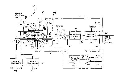
- Turning now to Fi~ure 23, the spring mass
sensor is connected in a first arrAngement to
ultimatelY determine acceleration applied to
~v~t 3R alona an axis of sensiti~itv Z. Of
WO90/lS997 PCT/US90/03059
2064213
-46-
course such axis of sensitivity may be oriented
along any axis, such as illustrated in Figures
20A-20C where accelerometers according to the
invention are placed on platform 1006 to be
sensitive to x and y platform axes.
The schematic of Figure 23 shows that mass
36' is supported from support 38 ~Jia sprin~s
havinq substantiallY equal sDring constants of
2ks. A d.c. voltage of plus v anfl minus V is
applied across sense conducting areas 90' on
plates of opposite support members 82', 84' which
of course are fixed with support 38.
A differential amplifier 120 has one of its
two inputs connected to lead 110 with another of
its leads connected to a reference voltage,
preferably ground. Lead 110 is connected to sense
conducting surfaces 90 of mass 36'. The voltage
appearing on lead 110 is proportional to the
Position of mass element 36' between the plates of
support members 82' and 84'. Consequentlv with
the ground reference applied to differential
amplifier 120, its output on lead 112 is a sense
displacement signal proportional to the distance
that mass element 36' has moved from a reference
position, halfwav between the reference plate of
2~ suPports 82, 84.
Two feedback loops are provided. The ~irst
includes a high pass filter 124', binary sampler
loop with binary feedback to force support plates
920'. The second includes a low pass filter 924
with analog feedback to "gimbal force" support
plates 922'. For each feedback loop, a constant
WO90/1~997 PCT/US90/030~9
206421~
-47-
charge is maintained on mass force plates 920 and
mass gimbal force plates 922 via leads 94 and 95
from charge generators 130 and 131. Such
generators are described above with reference to
Fiqure 15.
The low pass filter 924 and high pass filter
124' are illustrated by wav of their freauenc~
responses in Figures 25A and 75~. The low
frequency analog loop includes low-pass filter 924
which has a high frequency cut-off frequency of
about .7HZ. Its response increases in attenuation
at frequencies above such cut-off frequency at a
rate of about 20db per increasing decade of
freauencv.
The delta-sisma binarv bit stream loop
includes high-pass filter 124' which has a low
frequencv cut-of, frequency of about ?O~HZ at
about 20db per decreasing decade of frequencv.
Its response decreases in attenuation at
frequencies below about 70OHZ. Filters 924 and
124' mav be realize~ bv filter circuitrv well
known in the art of analog filter design.
Returning to Figure 23, the displacement
error signal after amplification and hiqh pass
filtering is applied on lead 126 to binary samPler
150 which produces a serial binary bit stream on
lead 168. That bit stream, representative of the
displacement of mass 36' in response to
acceleration, is applied via lead 164 to top
support force plate 920', while the complementary
binarv bit stream on lead 166 is applied to bottom
supPOrt force plate 920'. Such binarv bit
WO90~15997 PCT/US90/03059
20642 1 ~
-48-
voltages applied to top and bottom force plates
920' and the constant charge applied to mass force
plates 920 cause mass 36' to move in a direction
to null the voltage or "VERROR" on lead 110. Such
high frequency loop is effective at frequencies
passed bv filter 124.
The low frequencv loop responds to
accelerations passed by filter 924. The
displacement at such frequencies are filtered via
filter 924 and applied via lead 926 to amplifier
928, where a voltage of opposite sign to the input
voltage on lead 926 is applied via lead 930 to top
support gimbal force plate 922' and a voltage of
the same sign is applied via lead 932 to bottom
support gimbal force plate 922'. Such analog
1~ voltages applied to top and bottom qimbal force
plates 922' and the constant charge applied to
mass gimbal force plates 920 cause mass 36' to
move in a direction to null the voltaqe or
"VERROR" on lead 110. Such low frequency loop is
effective at low frequencies passed bv ilter 924.
As will be apparent to one of skill in the
field of negative feedback or automatic feedback
controls as applied to sensor design, each of the
two feedback loops must be stable. Depending on
2~ the components used to implement the low frequency
loop and the delta-sigma binary bit stream loop of
Figure 23 (and of other loops presented herein),
it may be advantageous to provide a lead
compensator in one or both loops. A simple lead
compensator may be combined with filter 124', for
example in the binar~T loop, if a stabilitv
WO90/1~997 PCT/US90/03059
20642 1 3
-4g-
analYsis of the loop so requires, of the form of a
parallel resistor Rl and capacitor C followed by a
resistor R2 to ground. The output/input relation
G(S) of such a lead compensator,
written in terms of Laplace transform operator S
is of the form
S ~ l/T
(`. ( S ~ =
S + 1/~T
where T = RlC,
a = R,, / ~1 + R2 .
When used in the application as illustrated
in Figures 20A-20C, the accelerometer of Fiqure ~3
effectivelv uses the low frequencv analoa feedback
loop to separatelv measure the low frequencv
gravitational effects on ~latform 1006. Thus, the
terms "electronic gimbal" and "~imbal" force
plates are a~plicable. The high frequencv
feedback loop of the accelerometer measures high
frequencY accelerations along the xp and yp axes
of platform lnO6, independent of the qravitational
2~ acceleration caused bv tilt. In effect, the
platform is electronicallv qimbled (as if it were
mechanically oriented to be perpendicular to the
true gravitY vector), to eliminate substantiallv
the effect of tilt and gravitv. Of course, the
low frequencv loop or electronic gimbal reduces
the required dYnamic range of the higher frequencv
WO90/15997 PCT/US90/03059
- 206~213
-50-
measurement of accelerations due to a sound
source.
Fi~ure ~6 illustrates other components of the
svstem used in coniunction with accelerometers
1010 (accelerometer Ax) and accelerometer 101~
(accelerometer Av) which are o~ the desiqn of
Figure ~3 (or the alternative designs discussed
previouslv or below). The output of the high
frequency loop on lead 168' is a serial binar~ bit
stream representative of acceleration due to sound
source S along platform axis xp. It is applied to
digital computer 1014. The output of the low
frequencv loop on lead 930' is an analog
representation of acceleration due to
gravitational acceleration along the platform axis
l~ xp du~ to the tilt of platform 1006. Tt can be
digitized bv a simple conventional analog to
diqital converter or the amPlifier could he
replaced with the binarv sampler to orm a low
frequencv ~-~ loop.
Similarly, accelerometer 1012 produces a
serial binarv bit stream on lead 168''
representative of the acceleration due to sound
source S along platform axis vp. The output of
the low frequencv loop on lead 9~0'' is an analog
representation of acceleration due to
gravitational acceleration along platform axis vp
due to the tilt of platform 1006. The analog
signals are applied respectivelv to A/D converters
1014 and 1016 to produce digital representations
30 of gxp and gyp~ the measured gravitational
accelerations along the x and v platform axes.
W090/l5997 PCT/US90/030S9
206421 3
Digital computer 1018 is programmed to
determine the tilt angles ~x and ~y from the known
magnitude of the gravitational acceleration of the
accelerometer in an untilted platform. After
determination of such angles ~x and ~y, the
accelerations axp and ayp are converted to
untilted accelerations along x and y axes of the
platform. Of course, ancillary measurements of
the angular orientation of the x and y axes of the
platform are necessary due to the floating buoy
and suspended platform. Such orientation may be
determined by mounting a compass on such platform.
With such compass information, accelerations
determined as above along untilted x and y axes of
the platform 1006 may be translated to provide an
acceleration vector in the direction of sound
source S.
The alternative accelerometer embodiment of
Fiqure 24 is similar to Figure 73, but applies
constant voltage V2, -V2 across top and bottom
force support plates 920'. The serial binary bit
stream on lead 168 is applied via lead 128' to
charge generator 130' which applies a
corresponding serial bit stream of charge to mass
force plates 920 via leads 94. The analog signal
2~ is provided in a manner identical to that of
Figure 23. The embodiment of Figure 24 may be
used as accelerometers 1010 and 1012 as discussed
above.
It is apparent that the embodiments of
3~ Figures 73 and 24 mav be modified to use a.c.
- WO ~115997 PcT/us90/03059
20642 1 3
modulation in a manner described in Figures 18 and
19 as discussed above.
Various modifications and alternatives in the
described structures will be apparent to those
skilled in the art of the foregoing description
S which does not depart from the spirit of the
invention. For example, although the preferred
method of fabricating the force transducer is by
chemical etching of a semi-conductor wafer, plasma
etching may also be used effectivelv. Although
the preferred N doping of the spring bases and
other regions is arsenic, boron or phosphorous may
also be used depending upon the original crvstal
tvpe. Although the preferred method of sensing
the displacement of the mass of the
mass-spring-support system is bv electric field
means, a displacement signal representative of the
position of the mass between the top and bottom
support plates may be generated by piezoresistors
or piezoelectric elements disposed on or in the
springs which change their resistance or output
voltage depending on the flex of the springs. A
current through such piezoresistors would produce
a voltage signal used in the same way as the
voltage signal of the source cond~cting plates as
described above with the preferred embodiments of
the invention. For this reason, these changes are
desired to be included in the appended claims.
The appended claims recite the onlv limitations to
the present invention and the descriptive manner
which is emplo~ed for setting forth the
PCI /US90/03059
WO90/15997
20642 1 ~ -
embodiments and is to be incorporated as
illustrative and not limitative.