Note: Descriptions are shown in the official language in which they were submitted.
TranslatiOn:
DEVICI~ I)ING A ~IER MI~ER, A Sl~lqICOl~DUCTOR IASE:R
D I,~ADS
The invention relates to a device including a semicon-
ductor laser and leads according to the preamble of claim 1.
For optical data transmi~sions over light waveguides,
opto-electronic transducer modules are required as transmit-
ter or receiver modules. In addition to other electrical
components, the transducer modules include, in particular, a
device equipped with a semiconductor laser that serves either
as transmitter or as receiver and is applied to the top
surface o~ a carrier member. Leads al~o applied to the
carrier member serve as elactrical connections for the
semiconductor laser
German Published~Patent Application DE-A1 4,013,630
discloses Buch a device that incIudes a semiconductor laser
and leads. The carrier membar i5 made of silicon. ~he
semiconductor~laser i5~ connected directly with a first lead
and by way of~a conna~ting wira, with~a second laad. ~his
device ha~ th~ drawbaok that it is suitable for optical data
tran~nission at most up to the MH2 range.
-
,"
., .
:.
2 ~
It is the object o~ the invention to provide an arrange-
ment including a semiconductor laser and leads which is
suitable for optical data transmissions in the highest
frequency range.
This is accomplished as defined in claim 1.
Features of the invention will become evident from the
dependent claims.
Instead of silicon, the invention employs a ceramic
material for the carrier member. Ceramic m~terials, ~or
example aluminum oxide tA1203) ceramics, have the advantage
over silicon o~ having a much higher specific electrical
resistance. For example, the specific resistance of alumi-
num oxide ceramics is higher at least by a factor of 108
than that o~ an undoped, that is, semi-insulating silicon. --
Compared to semi-insulating gallium arsenide, the specific
resistanco o~aluminum oxide aePamics is higher at least by a
factor o~ 104. Due to the lower specific resistances,
ilicon and gallium arsenide, when employed as substrates for
leads, exhibit high leakage losses if high or extremely high
frequency electrical~signals propagate through the leads. ~i
: ~ :
Another drawback o~ silicon is that the purity of the
carrier member realized during manufaoture is lost agaln in
subsequent proaesses for producing the leads. ~ j
, '
: ~
:: ~ .
~0~3~9
In high temperature diffusion processes or in the
production of layers in a vacuum vapor depositing system, the
silicon is enriched with impurities, thus reducing its
specific resistance. Particularly suitable ceramic materials
for the carrier member are aluminum nitride and boronitride.
Both materials exhibit high thermal conductivity. Addition-
ally, aluminum nitride has a coefficient o~ thermal expansion
which approximately corresponds to that of the substrate
(indium phosphide) of the semiconductor laser.
According to one embodiment o~ the invention, the
semiconductor laser is applied to the edge of the surface of
the carrier member in such a way that no percentage of the
transmi6sion light emitted by the semiconductor laser is
absorbed or reflected by the surface of the carrier member.
Instead, thanks to the manner of attachment o~ the semicon-
ductor laser, it is possible to easily adjust a light
waveguide with regpect to the beam of transmitted light.
In a pre~erred embodiment, the microstriplines are
terminated by ohmic resistors which are adapted to the
characteristic impedances of the microstriplines. The ohmic
resistor~ are here attached to the carrler member at a
location xemote ~rom the semiconductor laser so as to prevent
the æemiconductor laser ~rom being additionally hsated by
the heat generated by the resistors.
- 3 -
~ ' : -
In a further preferred embodiment, a direct current and
an alternating current composed of the electrical high
frequency signals are supplied to the semiconductor laser
through separate lines. This has the advantage that the
lines can be adapted ~pecifiaally to the type of current and
a terminating resistor is not charged with direct current.
The device according to the invention is suikable for
high frequency signals at a frequency of more than 20 GHz.
Other advantageous features of the invention will become
evident from the remaining dependent claims.
The invention will now be described with reference to
embodiments thereof that are illustrated in the drawing
figuras. It i6 shown in:
Fig. 1, a plan view of a first device including a
semiconductor laser and microstriplines
,:. . ~, ...
attached to the top surface of a carrier
member;
Fig. 2, a coil formed by a microstripline;
Fig. 3, a side view of the first device; and
Fig. 4, ~ a plan Yiew of a second device.
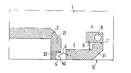
Figure 1 shows the first device which includes a carrier
member composed of a ceramio material, for example of
aluminu~;nitride (AlN~ or boronitride (BN), and has the
shape of a blocX 1. On it microstriplines 2, 3 and 4 are
, ~
4 -
'' ':
:
.- 2 ~
provided as leads. Microstripline 2 serves as the lead for
high frequency signals that are superposed on a direct
current for a semiconduotor laser 5. Semiconductor laser 5
is operated by the direct current and is modulated by the
high frequency signals. Semiconductor laser 5 is soldered
onto a region 20 of microstripline 2. Its underside is
metallized and serves as electrical contact with region 20
of microstripline 2. on its top surface, the semiconductor
laser is provided with a ~urther electrical contact 50 which
is connected with microstripline 3 by way of a bonding wire
6. Together with the electrical components downstream of it
when seen in the direction of transmission of the high
frequency signals, microstripline 3 serves to conduct the
high frequency signals to a ground contact. By way of an
ohmic resistor 7, microstripline 3 is connected with micro-
stripline 4. The latter forms the edge outline of a bore 8
that is elactrically conductively plated to its cylindrical
interior wall.
Microstriplines 2 and 3 have a compensated bend 21 and
31, resp~ctively, in order to keep reflection of the high
frequency signals low~ Such compensated bend~ 21, 31 are
customary in ~crowave circuits and are disclosed, for
example, by R. K. Ho~mann, in "Integrierte Mikrowellenschal-
; -~5 -
.
... .. . . . . . . . . . . .
S '~ ~ ~ 9
tungen" [Integrated Microwave Circuits], Berlin, Heidelberg,
New York, Tokyo (1983), page 97.
Microstripline 2, ~or example, has a characteristic
impedance of 50 n. It should there~ore be terminated by an
ohmia resistor of 50 n. I~, however, an ohmic resistor were
included betw~en microstripline 2 and semiaonductor laser 5,
the heat generated in the latter would have an influence on
the characteristics o~ semiconductor laser 5.
Since, however, semiconductor laser 5 constitutes, for
example, an ohmic resistance of 5 Q, micro~tripline 3, which
lies downstream of semiconductor laser 5 in the direction o~
transmission of the high frequency signals, must have a
characteris~ic impedance o~ ~5 n in order to ~orm, together
with semiconductor laser 5, a 50 n~terminating resistance for
microstripline 2. .- .
Since miarostripline 3 nowAhas a characteristic im~ ~ ~ i
pedance of 45 n, it requires an ohmic terminating res1stance
of likewise 4S n; thi is~resigtor 7.
.
;~ Semiconductor laser 5 is arranged on~ block 1 in such a
manner that it is flush with one side edge 10 of block 1.
The transm~tting light generated by semiconductor laser 5 ~s ;.
:: : : : : :~`
emitted through the it~ transverse side disposed on side edge
10.
6 -
,. .
Instead of a single bonding wire 6, a plurality of
bonding wires may be provided to connect semiconductor laæer
S and microstripline 3. Since a bonding wire as electrical
component ess~ntially constituteC; an inductance, such
inductance can be reduced if several bonding wires ~orm the
connection betwean semiconductor laser 5 and microstripline
3.
From this microstripline, the direct current component
and the high frequency signals can be transferred separately
to microstripline 4 i~ an inductive component 9, her~ shown
for the ~ak~ o~ simplicity as a co.il formed by a wire, is
provided in parallel with resistor 7.
Pre~erably, component 9 (Figure 2) is Pormed by a coil
which is connected, on the one hand, with microstripline 3
and, on the other hand, by way of a bonding wire 90, with
microstriplina 4. In this case-, component 9 is configured
either as a microstripline or as another lead.
Figure 3 i~ a schematic representation of the layer
structure on block 1 (not to scale). Microstriplines 2 to 4
are each composed of three sup~rposed layers: an adhesive
layer 11, a solder layer 12 and a protective layer 13.
Adhe~ive layer 11 is composed of a nickel-chromium alloy,
solder 13yer 12 of nickel and protective layer 13 of gold.
- 7 - :
~ ~3 ~
Adhesive layer 1~ and solder layer 12 are pre~erably
vapor-deposited onto block 1, pro~ective layer 13 is applied
electrochemically. Only adhesive layer 11 and solder layer
12 are present in region 20. In part of region 20 on solder
layer 12, a layer sequence 14 containing gold and tin is
applied on which semiconductor laser 5 is disposed.
Ohmic resistor 7 i5 formed in that the adhesive layer 11
is the only layer present there. On its underside, block 1
is covered by a layer 15 serving as ground contact. The
interior wall of bore ~ (not shown in Figure 3) is likewi;se
covered by adhesive layer 11, solder layer 12 and protective
layer 13.
In a second device shown in Figure 4, the leads for the
direct current and those for the alternating current are
separated from one another. The high frequency signals are
supplied to semiconductor laser-5 through microstriplin~ 2 by
way of a capacitor 16, a microstripline 17 and region 20 of
microstripline 2. Capacitor 16 serves to electriaally
separate the direct current component from microstripline 2.
The direct current component iB supplied to semiconductor
laser 5 through a line 18, an ohmic resistor 19, a line 22,
an inductive component 23 as well as microstripline 1~ and
region 20. ~h~e inductive component ~3 is preferably con-
figured in the mannar shown in Figure 2.
. .
.. . .. . . .
: : ,~., .. :
- : :':; ~
12 are present in region 20. In part of reglon 20 on solder
layer 12, a layer sequence 14 containing gold and tin i5
applied on which semiconductor laser 5 is disposed.
Ohmic re6istor 7 i~ ~ormed in that the adhesive lay~r 11
is the only layer present there. On its underside, block 1
is covered by a layer 15 serving as ground contact. The
interior wall o~ bore ~ (not shown in Figure 3) is likewise
covered by adhesive layer 11, solder layer 12 and protective
layer 13.
In a second device shown in Figure 4, the leads ~or the
direct current and those ~or the alternating current are
separated from one another. The high frequency signals are
supplied to semiconductor laser 5 through microstripllne 2 by
way of a capacitor 16, a microstripline ~7 and region 20 o~
microstripline 2. Capacitor 16 serves to electrically
separate the direct current component from microstripline 2.
The direct current component is supplied to semiconductor
laser 5 through a line 18, an ohmic resistor 19, a line 22,
an inductive component 23 as well as microstripline 17 and
region 20. ~he inducti~e component 23 is preferably con-
figured in tha manner shown in Figure 2.
- .
-:
:
,.......... : , ' , ' : . :
.: . ` : ; ~ ~ :
,,
,: . .
~' ' ' :
' : ,