Note: Descriptions are shown in the official language in which they were submitted.
This invention relates to a method of preparing
semiconductor wafers with good intrinsic Bettering
capability for use in CMOS devices, especially highly
ar,~timony-doped epitaxial wafers.
Metallic contaminants in semiconductor substrates kill
minority carriers, causing latch-up in bulk wafers and
adversely affecting oxide and diode integrity in epitaxial
wafers. It is therefore important to remove such
contaminants from the substrate. This can be achieved by a
process known as intrinsic Bettering, which involves
deliberately creating defects in crystal lattice by
incorporating oxygen atoms in the crystal. The oxygen atoms
combine with the silicon in the lattice to form Sio2 nuclei.
These create the crystal defects, which act as traps for the
metallic contaminants.
In practice, it has been found difficult to get oxygen
to precipitate in antimony-doped wafers because the antimony
retards the oxygen precipitation.
Intrinsic Bettering in substrates highly doped with
antimony, which are used for epitaxial wafers, is of major
importance, especially for ensuring gate oxide and diode
integrity. Efforts have been made to achieve good Bettering
in N/N+ antimony doped epitaxial wafers [See, for example,
J. O. Borland, and T. deacon, (Solid State Technology,
August 123 (1984)], but such efforts have generally been
hampered by the oxygen retardation [See, T. Nozaki and Y.
Itoh, J. Appl. Phys., 59, 2562 (1986)].
While some mathematical models explain the oxygen
retardation effect on the basis of electrical effects within
the crystal, more recently it has been observed [S. K. Bains
et al. , This Journal, 137, 647 (1990)] that crystal doped
with tin, which has a similar ion size to antimony, does not
- 1 -
exhibit this oxygen retardation behaviour, which sucJgests
that the retardation is not caused solely by the large size
of the antianony ions, as had previously been thought.
One method for achieving significant oxygen
precipitation generally in silicon wafers [See, for example,
W. Wijaranakula et al., This Journal, 129, 3133 (1988)] is
to grow oxygen nuclei or clusters at low temperatures (500-
800°C) prior to processing at higher temperatures where
oxygen precipitation occurs. At low temperatures,
nucleation is easier because of the lower thermal energy
available to break up the Si02 nuclei as they form. At
higher temperatures, oxygen diffusion increases and, for
nuclei above a critical size, which depends on the
temperature, growth occurs faster. Nuclei below the
critical size tend to shrink due to the increased thermal
energy to break up the bonds. Typical nucleation cycles are
carried at a constant temperature (650-750°C) for fairly
long time (8-48h.). This method has not proved very
effective for antimony doped wafers, and the long heat
treatment induces warping in the wafer, which is highly
detrimental to LSI processes.
Long treatment times at the low temperature (650°C) are
required to produce enough nuclei above the critical size
for growth during subsequent high temperature annealing.
Kishino [S. Kishino et al., J. of Appl. Phys., 23, L9, 1984]
showed that for lightly doped wafers the low temperature
treatment time can be reduced by employing a nucleation
growth (NG) cycle, wherein a treatment is first carried out
at 650°C for about 2 hrs. followed by a treatment wherein
the temperature is ramped up to about 900°C over a period of
1 to 2 hrs. Py ensuring that the rate of increase of the
critical size was lower than the growth rate of the nuclei,
Kishino was able to obtain high defect densities without
long cycle times.
- 2 -
~tJ~l~~~'v
Kishino carried out the NG cycle after an initial
denuding treatment at 1200°C for 3 h:rs. He did not address
the problem of oxygen retardation that occurs in strongly
antimony doped wafers.
An object of the invention is to provide a method of
preparing semiconductor wafers with improved Bettering
properties, especially wafers highly antimony-doped
epitaxial wafers.
In accordance with the present invention a high
temperature treatment is first carried out in on a
semiconductor wafer for between about 20 to 60 minutes to
form an initial oxidation layer on said wafer. The wafer is
then heated at a moderate temperature in an inert atmosphere
for about 1 to 4 hours to initiate crystal nuclei formation.
The nuclei are then grown by ramping up the temperature at a
rate of between about 1 and 10 °C/min, preferably 1 to about
3°C, to a temperature of at least about 850°C. Subsequently
well diffusion is carried out at temperature of at least
about 1000°C.
The wafer can be a silicon wafer highly doped with
antimony. Best results are obtained if during activation
the oxidation is wet (I32/o2) rather than dry (02).
The moderate temperature can be about 600-700°C,
preferably 650°C. The temperature is preferably ramped up
to a temperature of about 900 to 1000°C and the well '
diffusion carried out at a temperature of about 1175°C.
Activation temeprature can be different from 1175°C,
but needs to be above 1000°C. The time spent at the
activation temperature can bary, but the optimum time is
around 35 min.
- 3 -
Ramp rates can be to be as much as about 10°C/min, but
from about 5°C/min, different activation temperatures are
required.
The ramp part of the nucleation cycle need not be
linear. Ror example, it can be parabolic. If ~tha
temperature increase is non-linear, the maximum ramp rate
can be higher than 3°C below 850°C.
The substrate can be doped with materials other than
antimony, and need not be highly doped. Indeed, the
invention can be applied to elements other than oxygen and
silicon, in which case the temperatures may vary.
Activation and nucleation need not be part of the same
furnace cycle.
Thus in a preferred embodiment the invention consists a
brief activation (?.0-60 mins. oxidation at 1175°C), a
nucleation soak cycle (soak at 600-700°C for at least two
hours), and a nucleation ramp cycle (linear increase in
temperature from 600-700°C to at least 850°C at a rate no
faster than abour 3°C/min.
It has been found that by following the initial wet
oxidation treatment of short duration by a camped nucleation
growth cycle, a significant improvement in oxygen
precipitation can be achieved bulk material, and good
results can be obtained in epitaxial wafers, including
antimony-doped epitaxial wafers.
Thus the method described permits the nuclation of
interstitial oxygen in lighly or hoghly doped silicon (with
antimony or other dopant) within a reasonable time (about 6
hours). After nucleation, a high level of interstitial
oxygen precipation can be achieved in the silicon during
~~~~~!~~~
device fabrication.
The invention will now be described in more detail, by
way of example only, with reference t:o the accompanying
drawings, in which:-
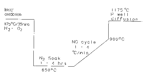
Figure 1 is a diagram showing the process steps of a
process in accordance with the invention;
Figure 2 is a chart showing the oxygen precipitation
after tamping to 900°C+
Figure 3 is a chart showing the oxygen precipitation
after tamping to 1000°C;
Figure 4 is a chart showing the number of bulk defects
after a ramp up to 900°C;
Figure 5 is a chart showing the number of bulk defects
after a ramp up to 1000°C;
Figure 6 is a diagram showing the finite size effect
when counting defects from an etched section; y
Figure 7 shows the number of bulk stacking faults per
unit volume corrected for bulk stacking fault size for
different combinations of nucleation growth cycles after
tamping to 900°C.
Figure 8 shows the number of bulk stacking faults per
unit volume corrected for bulk stacking fault size for
different combinations of nucleation growth cycles after
tamping to 1000°C.
Figure 9 shows the correlation between stacking fault
size and density corrected for defect size;
- 5 -
Figure 10 shows the number of defects per unit volume
for different combinations of nuclear growth cycles with
ramping to 900°C;
Figure 11 shows the number of defects per unit volume
for different combinations of nuclear growth cycles with
ramping to 1000°C;
Figures 12 and 13 show the precipitated interstitial
oxygen (DELTA Oi) as a function of initial Oi for high
oxygen epitaxial wafers and bulk wafers;
Fig. 14 is a schematic representation of the splits for
batch E9-8 for the three micron process. Wet inital
oxidation was done at 1175°C;
Fig. 15 is a schematic presentation of the splits of
lot E9-8 for the 2 micron process. Initial oxide is grown at
950°C;
Fig. 16 shows preaipitate~cl interstitial oxygen (DELTA
[Oi]) for bulk wafers with nucleation after HCI initial
oxidation as a function of initial [Oi];
Fig. 17 Precipitated interstitial oxygen (DELTA [Oi])
for epitaxal wafers with nucleation after HCI initial
oxidation as a function of initial [Oi];
Fig. 18 shows precipitated interstitial oxygen (DELTA
[Oil) for bulk wafers with nucleation before HCT initial
oxidation as a function of initw [Oi];
Fig. 19 shows precipitated interstitial oxygen (DELTA
[Oil) for epitaxial wafers with nucleation before HCI
initial oxidation as a function of initial [Oil;
- 6 -
Fig. 20 shows precipitated interstitial oxygen (DELTA
[Oil) for bulk wafers with nucleation before wet init3.a1
oxidation as a function of initial [Oi];
Fig. 21 shows precipitated interstitial oxygen (DELTA
[Oi]) for epitaxial wafers with nucleation before wet
initial oxidation as a ftinction of initial [Oi];
Fig. 22 shows precipitated interstital oxygen (DELTA
[oil) for bulk wafers with nucleation after wet initial
oxidation but before soak, as a function of Oio;
Fig.23 shows precipitated interstitial oxygen (DELTA
[Oil) for epitaxial wafers with nucleation after wet initial
oxidation but before soak, as a function of Oio;
Fig. 2~ shows the probable dependence of precipitation
on time spent at 11750 as deduced from results of this
experiment. Full line is for epitaxial wafers, broken line
is for bulk;
Fig. 25 shows precipitated interstitial oxygen (DELTA
[oi]) for epi HiOX wafers with 2pm initial oxidation as a
function of initial [Oil;
Fig. 26 shows precipitated interstitial oxygen (DELTA
[Oi]) for epi HIOX wafers with nucleation after 2pm initial
oxidation as a function of initial [Oi];
Fig. 27 shocas precipitated interstitial oxygen (DELTA
[Oi]) for epi HIOX wafers with nucleation before 2pm initial
oxidation as a function of initial [Oil;
Fig. 28 shows precipitated interstitial oxygen after p-
well diffusion as a function of precipitated oxygen after
initial oxidation for epi I-liOX wafers (box) and for bulk
- 7 -
wafers (cross) (3 micron process);
Fig. 29 shows bulk defects and denuded zone of
epitaxial wafers with HCI initial oxidation followed by
nucleation (split A). Scale is 220X. Denuded zone depth is
about 65pm. Wafer's surface is at the left;
Fig. 30 shows bulk defects and denuded zone of
epitaxial wafers with HCT initial oxidation followed by
nucleation (sp7.it A). Scale is 220X. Denuded zone depth is
about 65pm. Wafer's surface is at the left;
Fig. 31 shows bulk defects and denuded zone of bulk
wafers with HCI initial oxidation followed by nucleation
(split A). Scale is 220X. Denuded zone depth is about 351mn.
Wafer's surface is at the left;
Fig. 32 shows bulk defects and denuded zone of
epitaxial wafers with nucleation followed by HCI initial
oxidation (split H, identical to C). Scale is 220X. Denuded
zone depth is about 30~m. Wafer's surface is at the left;
Fig. 33 shows bulk defects and denuded zone of bulk
wafers with nucleation followed by HCI initial oxidation
(spht B, identical. to C). Scale is 220X. Denuded zone depth
is about lopm. Wafer's surface is at the left;
Fig. 34 shows bulk defects and denuded zone of
epitaxial wafers with wet initial oxidation followed by
nucleation and soak (split D). Scale is 220X. Denuded zone
depth is about 25;im. 6Vafer's surface is at the left; and
Fig. 35 shows bulk defects and denuded zone of bulk
wafers with wet initial oxidation followed by nucleation and
soak (split D). Scale is 220X. Denuded zone depth is about
2opm. Wafer's surface is at the left.
_ g _
Referring to the drawings, as shown in Figure 1, 'the
wafers, which can be highly antimony-doped epitaxial wafers,
are first subjected to a wet oxidation at 1175°C for 35
mi.ns. This creates an initial oxidation layer.
Tn a second phase, the wafers are subjected to a N2
soak at 650°C for 1 - 4 hrs. This soak causes diffuse the
Si02 nuclei to diffuse into the substrate.
In the next step, the temperature is ramped up to
1175°C over about 2 - 10 hrs. to initiate nucleation growth,
after which P well diffusion is carried out a temperature of
1175°C for about 400 wins. in the presence of oxygen.
Example 1
One hundred 100mm n-/n+ epitaxial wafers were used with
substrates antimony-doped to 30-50 mSZcm. The epitaxial
layer was lightly doped with phosphorus and nominally 10
microns thick. The oxygen content of each wafer was
measured before any processing was done. All wafers were
within 15.7-16.3 pptua (Atomic part per million) range (ASTM-
F121-83). Carbon content was specified to be less than 1.0
ppmA. The substrate used for these wafers is somewhat less
heavily doped than the usual antimony doped epitaxial
substrate (8-15 m~cm), and this enabled the oxygen content
to be measured by conventional infra-red techniques.
Because of the lower doping level, some oxygen precipitation
has been found to occur in similar substrates when long
nucleation times are used.
Tn the example, the most important front end thermal
cycles, namely, initial oxidation, nucleation-growth (NG),
well diffusion and field oxidation were~carried out in
sequence. In an actual process subnitride oxidation and
nitride deposition take place before field oxidation.
- 9 -
Studies of the evolution of oxygen precipitation hare shown
that this difference is not significant for oxygen
precipitation, even 'though nitride deposition is carried out
at a temperature close to 80o°C, at which interstitial
oxygen may precipitate.
Nucleation-growth (NG) was inserted after initial oxide
(1175°C/35min.) and before well diffusion (1175°C/400min.) .
By contrast in Kishino, the NG cycle was carried out after a
treatment at 1200°C for 3hrs. and before a treatment l6hrs.
at 1000°C for 16h. These differences in processing
temperatures and times lead to the differences in oxygen
precipitation. Oxygen nucleation is retarded if long times
are spent at high temperatures before NG is carried out.
The following experimintal NG cycles were carried out.
The nitrogen soak was carried out at 650°C for periods
of lhr., 2hr., and 4hr. Ramping from 650°C up to 900°C or
1000°C was tried with at 1.0°C/min., 2.0°C/min., and
4.0°C/min. Total cycle times were between 122.5 and 590
minutes. Two wafers were used per split.
Twelve wafers were also processed without an NG cycle
to serve as references. Two of these wafers had a very high
oxygen content, about 21 pptua.
_ 10
Table 1
Total NG Cycle Time
Ramp to 900C
Soak @ 650C 1.0 hr. 2.0 4.0
hr. hr.
4.0C/min. 122.5 182.5 302.5
2.0 C/min. 185.0 245.0 365.0
1.0C/min. 310.0 370.0 490.0
Ramp to 1000C
Soak @ 650C i.hr. 2.0 hr. 4.0 hr.
4.0C/min. 147.5 207.5 327.5
2.0 C/min. 235.0 295.0 415.0
1.0 C/min. 410.0 470.0 590.0
Wafer bow was measured using interferometry and the
final interstitial oxygen content was measured by infrared
spectrophotometry (ASTN-x'1,21-83) . Then the wafers were
cleaved and were given a Wright etch for 1.0 minute to
delineate surface and bulk defects. Phase contrast pictures
of wafer sections were taken near the wafer centre to count
bulk defects (precipitates, and stacking faults). Some
pictures were also taken near the wafer edges for
comparison.
- 11 -
~~~L~!~~~v
Most often, gettering ability can be evaluated by any,
of four methods: 'two indirect, one relative and one
absolute. In this work the two indirect methods and the
relative method were used. The two indirect methods consist
in: measuring the amount of precipitated oxygen after
simulated processing (~Oi), and cc>unting the number of bulk
defects after preferential etching of a section. The
relative method consists of processing a number of wafers
with standard processing and wafers with experimental
processing. Results from each split are then compared for
gate oxide and/or diode integrity.
The absolute method consists of intentional~.y
contaminating a sample and measuring the amount of
electrically active contamination after processing. This
method was not used in this experiment.
Oxygen precipitation results are shown in Fig. 2,
Cramping 900°C) and Fig.3 Cramping to 1000°C). A change of
1.0 pptua in interstitial oxygen concentration was observed
on wafers without NG (with identical initial oxygen
content). Part of the interstitial oxygen loss is due to
oxygen out diffusion (0.5 ppmA calculated). Ramping to
900°C or to 1000°C made little difference except when the
ramping rate was 2.0 C/min., in which case ramping to 1000°C
yielded significantly higher oxygen precipitation for all
three soak times.
The oxygen precipitation is significant in these
epitaxial wafers. Each wafer used for NG had an initial
oxygen content between 15.7 to 16.3 pptua (1&.0 pptua will be
assumed in the following discussion). The least amount of
precipitation (~oi=3.5 pptua) observed with NG (lh/650°C and
4.OC/°min. ramp up to 950°C) is about six times higher than
the simulated process with no NG cycle (excluding oxygen
outgassing).
- 12 -
~~~~~!~r~C~
Wafers with Oi=21 pptua which did not have NG showed D
Oi=4 pptua, which is comparable to the least amount of
precipitation observed with NG. The greatest precipitation
observed with NG (~Oi=10.8 pptua) was obtained on wafers
haling a 4.Oh, soak and tamping at 1.0°C./min. up to 1000°C.
Such a level of precipitation page leaves a mere 5.2 pptua of
interstitial oxygen in the wafer.
The solubility limit of oxygen at 1000°C (Field
oxidation) is about 2.6 pptua, and at 1175°C (Well drive) is
8.2 ppmA. An interstitial oxygen residual level of 5.2 pptua
indicates that some level of precipitation must occur during
field oxidation for the described process (5.2 pptua is less
than the 8.2 pptua predicted by the solubility limit at
1175C). If this is the case, then precipitate growth must
occur during P-well diffusion. The maximum ~Oi possible
after well diffusion (400 min. @ 1175°C) is 7.8 pA
(solubility limit is 8.2 pptua). Preliminary step by step
studies of precipitation confirm this hypothesis.
Precipitate growth during wall diffusion probably slows
down near Boi = 7-8 pptua, because the interstitial oxygen
concentration is very close to the solubility limit and
because precipitation kinetics are strongly dependent on
supersaturated Oi concentration. This can explain the
saturation effect observed in Fig.3 for slower ramp rates.
It also explains why curves for different soak times seem to
converge to about 11 pptua (maximum DOi after field
oxidation). Once all the curves are merged together, the
increase could continue asymptotically to ~Oi maximum, about
13.4 pptua, if more time was spent at 1000°C.
In the process sequence used here no significant time
is spent at temperatures below 900°C without an NG cycle.
Such low temperatures (600°C-800°C) cause oxygen
nucleation.
This indicates that: precipitation is controlled by a low
13 _
~~~~~~~3~
temperature mechanism (nucleation) under the conditions used
here. It has been shown that heterogeneous nucleation can
also be enhanced by subjecting the wafer to a high
temperature (1280°C) before nucleation, presumably by point
defect clusters. In the case studied here, such a mechanism
is also conceivable because a high temperature (1175°C)
cycle precedes nucleation.
In order to estimate the most: efficient use of furnace
time versus oxygen precipitation, calculations of the ratio
of oxygen precipitation to the square root of extra furnace
time were carried out. The results are shown in Table 2.
Table 2
Optimum NG Cycle Analysis
Rsmp t~ 900C
Soak @ 650C 1.0 hr. 2.0 hr. 4.0 hr.
4.0C/min. 23 37 44
2.0 C/min. 46 49 45
1.0C/min. 38 40 41
Ramp to 1000C
Soak @ 650C l.hr. 2.0 hr. 4.0 hr.
4.0C/min. 25.5 39 40
2.0 C/min. 42 47 43
_ 14 _
~~~~~~~3
1.0 °C/min. ~ 39 44 39
The square root of time is arbitrarily used because
extra time is less important, ira this case, than the end
result, precipitation of oxygen. According to Table 2, the
cycle which provides the optimum ratio of oxygen
precipitation to the square root of extra furnace time is
2h. at 650°C and 2.0°C/min. ramp-up to 900°C.
The standard method used to estimate the bulk defect
density assumes that: (i) exac~t7.y 1.0 micron of silicon was
etched; (ii) the sample picture area (3.0 X 10⁻³cm2) is
representative of the wafer; and (iii) that the defects are
smaller than 1.0 micron. The exact thickness of silicon
removed is only of relative importance because all the
wafers are etched at the same time and are expected to have
seen the same etch rate. On the other hand, the assumption
that the measured area is representative of the wafer, is
not rigorous. To avoid the effect of systematic spatial
distribution pictures were always taken near wafer centre.
The last assumption, that defects are smaller than 1.0
micron, is valid for oxygen precipitates that have been
shown to be typically less than 2000A, but not for bulk
stacking faults (BSF). The standard defect density
calculation does not take into account the size of BSF).
This will be shown later to lead to significant differences
in interpretation.
To understand a more about bulk defects, pictures of
wafer sections following a 1.0 minute Wright etch were
taken. Most of the visible defects at this scale were found
to be bulk page stacking faults (BSF) . A highly non-
uniform distribution of bulk defects was observed in wafers
with an initial oxygen content of about 20 pptua and not
- 15 -
~~'~'.~'~t~~~~
subjected to an NG cycle as a result of the initial non-
uniform spatial distion of heterogeneous nucleation centres.
In the wafers with NG the distribution of bulk defects is
very uniform across the wafer.
Using the standard method of calculation, the curves,
as shown in Figures 4 and 5, were found to flatten for ramp
rates of 1.0°C~min. A very unexpected affect is that higher
defect densities are observed for wafers which have been
subjected to l.Oh. N2 soak at 650°C.
An interesting feature of the results observed is the
range of different numbers and sizes of the defects seen.
Pictures taken at higher magnification revealed more details
about the bulk page defects in wafers which had slower ramp
rates. The most visible defects are small BSF and their
number is very large. In addition to small BSF (5-7 1im),
larger BSF (15-25 PM) can be observed (see Fig.5) near the
beginning of the denuded zone. When NG with faster ramp
rate to 900°C (Fig.lO) is used, numerous small defects ,
(likely to be oxygen precipitates) and some stacking faults
of larger size (15-20 Pm), are observed. Again here, even
larger BSF are located near the beginning of the denuded
zone.
When defect densities were computed, it was assumed
that defects were much smaller than the thickness of silicon
etched (l.O,um) . If this is not 'the case then the number of
defects is over-estimated. Figure 6 shows the number of
defects that out the horizontal line nr which are in the
etched volume. These defects appear after a preferential
etch. The smaller defects show a smaller count. As shown
in Fig. 6, defects which have their centres out of the
etched silicon layer, but extend in this layer, will appear
after the etch. Tn many pictures defects much larger than 1
micron are observed. Tn particular, this is the case for
- 16 -
~~~~~~c~
most bulk stacking faults.
This detrimental effect can be compensated by assuming
tta.at; (i) all BSF in the observed area have the same real
length (w); (ii) all BSF observed a:re circular in (111)
planes (z3); (iii) the thickness of silicon etched (1) is
exactly 1.0 micron; and (iv) the observed average BSF length
is w = rcw / 4. . Under these assumptions, the volume that is
considered for defect density calculation (V) is given by
V=~1+4wl~c) [1)
D=nlV [2]
and is strongly dependent on defect size. This volume
considers defects of length w located within the interval [-
w., 1+w] from the original surface (S) to be visible in all
cases.
Equation 2 permits an accurate calculation of the
defect density (D) knowing the number of defects (n) of
average size w. It was observed that the Wright etch failed
to identify clearly BSF which intersected the cleavage plane
(110) parallel to the 100 surface. This is rather unusual,
and is still unexplained. To correct for this effect and
because only two of the four possible BSF orientation were
observed, the number of BSF observed (n) was multiplied by
2.
Figures 7 and 8 show the corrected BSF density for
wafers which had l.Oh., 2.Oh. ar 4.Oh. soak at 650°C. The
defect density in these figure is at least half an order of
magnitude less than those calculated using the standard.
Also, variations from split to split seem more consistent
with oxygen precipitation data. In particular, wafers with
shoxter soak time at 650°C exhibit fewer BSF. From Figures
- 17 -
7 and s, it appears 'that a soak of at :Least 2. hrs. is
required to consistently give a large BSF density. This is
in agreement with results found from oxygen precipi'ta'tion
experiments (Figures 2 and 3).
From the above observations , it is clear that
neglecting defect size when evaluating defect density leads
to erroneous conclusions.
It is believed that a possible explanation for the
observed BSF size correlation with BSF density is that BSF
gro~~rth reaction is limited by the supply of reactants
(interstitial silicon). In this case BSF volume is
inversely proportional to defect density. This would
explain why BSF seen on wafers having a slower ramp rate
(higher BSF density) are smaller. The fact that larger BSF
are observed near the beginning of the denuded zone is
different, and can be explained by the larger supply of
interstitial silicon from surface oxidation during well
diffusion and field oxidation.
When the following conditions exist: (i) defects are
two dimensional (like extrinsic BSF) ; (ii) the supply of
reactant (Six) is the growth limiting factor; and (iii)
defect size is narrowly distributed, The relationship
between average defect size and defect density (D) is
governed by a quadratic power law
D = K1~1~V2 L
where K is a proportionality constant given by
K = ~cNiC~ l 4 [ 4 ]
where Ni is the number of SiI generated per unit
volume; CI is the increase in BSF surface caused by the
- 1$ -
~~.~~~ ~~%~ t~
addition of Sil in the extra 111 plane.
The relation between defect size and defect density
shown by Equation 3 is strong. Figure 9 shows the observed
relationship between BSF density and size for the same
wafers as in Figures 7 and 8. The BSF density was
calculated with the corrected method, taking into account
BSF size. Although some spread in the data points is
observed, a negative square law dependence at high defect
density fits the data very well, as expected from Equation
f~l.
Fig. 9 also shows the expected defect size saturation
at low defect density. This indicates that in wafers with
actual BSF density below 107 cm°3 the supply of interstitial
silicon is not the factor limiting BSF growth, but in this
case SiI capture is the limiting factor. Wafers processed
without NG show a BSF length of about 40 ~,m. This is the
maximum length which can be achieved for the growth time
allowed. For wafers without NG, the density is small,
typically about 105-106 cm°3.
Assuming that (i) a BSF is composed of an extra 111
plane {extrinsic stacking fault) ; (ii) the increase in BSF
area caused by the addition of an interstitial silicon atom
(C,) is the inverse of the number of atoms per unit area in
a 111 plane, e.g. 5.21 x 10°l6cm~/atom; (iii) that BSF
growth occurs during the well drive. ~Tsing the slope of
Figure 9 at densities above 107 cm°3 (K = 112cm-1 ), the
total number-of SiI generated per unit volume (NI) can be
calculated at 1175°C.
N~=4Kl(~cC~)=2.7x10¹⁷Silcm3 [5]
The total number of interstitial silicon atoms
generated can also be calculated from the quantity of
19 _
~~~~~c~~
precipitated interstitial oxygen. The general form of the
growth reaction of oxygen precipitates is given by Equation
(s]. Where Siv are silicon vacancies; y, the average number
of vacancies used to accommodate lattice space; of is
interstitial oxygen; and y2 is the average number of
interstitial silicon atoms ejected to accommodate lattice
space.
(1+yl+yz)s~ +2o~-~y,siv~s~ c~2-~-yzsl~
Assuming that: (i) volume accommodation is mainly
associated with Si, emission (this is supported by the
presence of BSF) ; (ii) interstitial oxygen solubility limit
is achieved during well diffusion (DOi = BOimax = 7.8 pptua);
(iii) volumetric requirement for Si02 (quartz) is 2.~5 times
that of crystalline silicon, for one Si atom, then the total
number of Siz generated by oxygen precipitation (R,) i.s
given by
Nr=~~i (2.25-1)/2=2.4x1~1'~''il/,~~3 f
The value obtained from equation 7 is in excellent
agreement with the experimental value calculated from the
dependence of BSF length on density.
The agreement between the results of Equation 5 and
Equation 7 suggests that the mechanisms assumed to describe
precipitation of oxygen in the experiment are valid.
Combining equations 5 and %, a relation between BSF size and
BSF density, which is only dependent on precipitated oxygen,
is obtained:
D=1.25~cc'r~~il8yvz t87
This expression enables the BSF density (D) to be
calculated knowing the amount of oxygen precipitated, and
- 20 -
~~3~yQ~~~~
BSF size. Of course, D is determined by the number of
nuclei whose size, obtained during nucleation, is above the
minimum size for growth at precipitation temperature.
Figures 10 and 11 show the volumetric density of the
small defects that are seen on high magnification pictures.
The same wafers as far Figures 7 and 8 were used. The
density of small defects is about 10 times higher than the
BSF density, and it varies less between splits. It also
appears that the small defect density .is somewhat
proportional to soak time.
Romping up to 900°C or 1000°C does not make much
difference in the density of small defects either, except
when the soak is only l.Ohr. In this case, the density of
small defects increases with slower romping rates, in
agreement with oxygen precipitation data. This tendency is
the opposite of what is observed for BSF density. From
this observation, it appears that the small defects are
oxygen precipitates that did not nucleate a BSF during well
diffusion.
From the observation that most of the small defects
(oxygen precipitates) grow during field oxidation, it is
interesting to ask how did oxygen nuclei survive the well
drive (1175°C) since interstitial oxygen is strongly
depleted (compared to the case where no BSF grow) after the
well drive. One possible answer is that interstitial
silicon depletion during well drive allows nuclei of smaller
size than normal to survive. These nuclei, or precipitates,
can then grow during field oxidation.
Because the mechanical strength of the wafers decreases
as interstitial oxygen concentration decreases, it is
possible that wafers warp during thermal processing. To
ensure that the enhance oxygen precipitation does not cause
- 21 -
~~~r~!~~~~~
this, bow was measured on all wafers. Tn all the cases the
processing induced bow was found to be less than 2 microns.
Of course this measurement is of limited use because the
normal process was not exactly followed. In particular most
of the bow occurs after the field oxidation because of the
nitride left on the back of the wafer, and nitride was not
used in this experiment. However it has been shown that
nitride deposition does not significantly affect wafer bow.
Because SiI is a by-product of oxygen precipitation,
depletion of SiI from the bulk caused by the high density of
BSF favours oxygen precipitation. This means that BSF
density and size control the oxygen precipitation rate along
with supersaturated interstitial oxygen concentration.
The interaction between dislocations and oxygen
precipitation has been noted before. In particular, high
pressure crystalline Si02 polymorphs (coesite) has been
observed in the form of small ribbons (25) along <110>
dislocations. Tt has also been observed that crystalline
phases of Sio2 are favoured by the presence of dislocations,
probably because of the high hydrostatic pressure around
dislocations. The presence of high density of BSF, in the
results presented here, explains why high levels of oxygen
precipitation are observed in highly antimony doped
substrate.
When BSF density (D) is high enough to affect BSF size,
the mean free path of silicon interstitial is strongly
reduced. Since fast metallic contaminants diffuse similarly
to silicon interstitials' they too should be captured by BSF
during cool down and see their mean free path reduced.
Therefore good Bettering is expected when the BSF length is
affected by the BSF density.
To confirm the improved Bettering of epitaxial wafers
- 22 -
?~~~~~~~
using NG, a lot of 21 wafers was processed with NG (9
wafers) and without NG (12 wafers) . On each finished
waters capacitors (8 sites) and diode integrity (5 sites)
was checked.
Capacitors (2,500,000 ,um2) were measured for leakage at
volts in accumulation (n-- and p- substrates). A
capacitor was considered short if a current greater than 30
nA was measured. The breakdown voltage of n+/p- diodes
(185,000 ~.m2) was measured at 1.0 pA. For the diodes the
fail criteria was a breakdown voltage below or equal to 21
Volts. The process used here usually gives n+/p- diode
breakdown voltage of 23 Volts.
Table 3 presents the results obtained.
Table 3
Capacitor and diode integrity test results
2.0 hr. anrl 2.0/05n. Ramp to 900O
Parameter Without NG With NG
Gate oxide leakage ~30nA 122.5 182.5
N+/p- diode breakdown <21V 185.0 245.0
The improvement in Bettering is measurable. The use of
NG has eliminated the occurrence of contamination induced
n-+-/p- junction soft-breakdown, and has reduced by about an
order of magnitude the density of gate oxide shorts. Even
considering the limited number of measurement sites and
wafers used the improvement is significant.
- 23 -
l
In summary, several nucleation cycles were experimented
with after an initial oxidation on N/N+ antimony doped
substrates. A11 these cycles show significant improvements
in oxygen precipitation. The cycle which provides the
optimum ratio of precipitation to extra furnace time
consists of 2hrs at 650°C in N2 with a ramp-up to 900°C at a
rate of 2.0°C/ min. (total extra time = 245min.). Total
oxygen precipitation obtained with this nucleation was about
9.0 ppmA for wafers with 1&.O ppmA of initial interstitial
oxygen content.
Significant improvements in oxygen precipitation and in
density of bulk defects show that nucleation-growth process
does improve the effectiveness of oxygen precipitation.
This in turn should greatly improve internal gettering in
wafers.
Fully processed wafers with and without ramp nucleation
were tested for gate oxide and n+/p- junction integrity.
For both electrical measurements a observed, confirming the
very significant improvement could be achieved with ramp
nucleation.
Example 2
Studies were carried out on the feasibility of
nucleation process standardization for epitaxial and bulk
material for a three micron process and the standardization
of nucleation process for two micron process with Poly back
sealed and HIOX epitaxial wafers.
A batch (E9-8) consisting of 42 prime wafers was
processed in according to the process flow in Figure 1. Bulk
and high oxygen content epitaxial wafers (epi HIOX) were
used for the 3 micron front end. Polysilicium back sealed
(PBS) and epi H7COX wafers were used for the 2 micron front
- 24 -
and. The wafers per material per split were used at all
times. Except for PBS, wafers had respectively 1.5, 16 and 7.7
pptua of initial interstitial oxygen content (Oio). Oio in
PBS wafers is not known.
Oxygen content was measured on bulk and epi HiOX wafers
before processing, after initial oxidation, p-well
diffusion, and field oxidation. Oxygen content in PBS wafers
cannot be measured because infrared absorption caused by
higher antimony doping (10- 20 m~2cm compared to 30-50 m~tcm)
is too important. In this case, PBS wafers from a single box
were used for all PBS splits.
In this experiment, it was decided to leave nitride on
the back of the wafers during field oxidation. This enables
a realistic evaluation of wafer warp during field oxidation.
It is also possible that tension caused by the nitride film
affects density and size of oxygen precipitates growing
during field oxidation. rilechanical stress may also affect
the size of BSF, but shotald not affect their density since
they are formed during p-well diffusion.
Wafer bow was measured by laser interferometry (Tropel
instrument), before processing, and after field oxidation
was completed and all oxide layers removed.
Fig. 14 graphically presents the splits done at initial
oxidation, nucleation, and soak. Split D is expected to be
the best compromise for high bulk defect density (BDD) bulk
and epitaxial wafers for 3 micron process. Split A is
thermally equivalent to what was already experimented.
Split D provided high BDD on epitaxial wafers. In ref.
1 no soak was done to shrink OSF. P-well diffusion, just
like the soak, is done at 1175~C following initial
oxidation.
- 25 -
Split B,-C and D are an attempt to generate BSF during
SPLIT A B C D E F
epi PBS X X
epi HIOX X X X X X X
Bulk X X X X
nucleation X X
ion 2~Cm X X
ion wet X X X
ion CH1 X X
nucleation X X X
soak X X
oxide etch X X X X X X
p-well dif . X X X X X X'
oxide etch X X X X X X
subnitox X X X X X X
nitride dep. X X X X X X
nitride etch X X X X X X
field oxide X X X X X X
oxide etch X X X X X X
nitride strip X X X X X X
oxide etch X X X X X X
initial oxidation. This would provide important internal
Bettering available during mask 10. However, for splits B
and C, nucleation without first denuding is risky for DZ
depth, if oxygen precipitates do not dissolve at 1175°C.
The table shows the experimental processing for this
batch. An X indicates the step was carried out. Two micron
field oxides were used on split E, F, and G.
This is the first time we conduct nucleation experiment
on the two micron process. This process does not use a
denuding cycle. The initial oxide is thin (200A) and is
grown at low temperature (9500C). However, it is believed
that this process can be adapted to internal Bettering with
epitaxial HiOX material.
Once the wafers were fully processed, they were cleaved
and one half of each wafer had a Weight etch [5] for 1.0
minute. This preferential etch reveals OSF, BSF,
- 26 -
dislocation, and precipitates, on the surface and on the
wafer section. Bulk defects are then counted and their
length measured.
Precipitation in bulk wafers i:~ different from in
epitaxial wafers. In particular, vex°y much reduced
precipitation was observed in epitaxial wafers during .field
oxidation (100a°C), even with nucleation.
Standard CHL initial oxidation with nucleation before
(split A: Fig. 16 and 17), or nucleation after (split B:
Fig. 5 and 6) gave results very much different from each
other. Precipitation is much better with nucleation done
before HC1 initial oxidation for bulk materials. Yet,
precipitation in epitaxial wafers is not very good in split
A and in split B.
This is an interesting result. For one thing, it
confirms the last experiment that spending too much time at
1175°C causes precipitation to be inhibited on bulk and on
epitaxial materials (split A). What is observed in split B
is that precipitation on epitaxial wafers is also degraded
when wafers do not spend any time at 1175°C before
nucleation. This clearly demonstrates the presence of an
optimum time to be spent at 1175°C before nucleation, to get
maximum precipitation in epitaxial wafers during p-well
diffusion.
In Fig. 18, bulk wafers show precipitation right after
initial oxidation. This indicates gettering capability just
after the first thermal cycle for wafers with Oio above 15
pptua. Lettering at this step helps decrease the density of
OSF growing during p-well diffusion. It also helps to getter
contaminants induced during mask 10.
Split C (Figs. 2C and 21) gave results nearly identical
- 27 -
to split B for both materials. This important similarity
shows that presence of CHL during initial oxidation does not
affects precipitation of interstitial oxygen.
Similarity between the results in Fig. 16 and the
results obtained with wet initial oxidation and soak done
before nucleation, also confirms 'the little impact that HC1
ambient has on nucleation or precipitation. This is an
unexpected conclusion since CHL oxidation increases denuded
zone (DZ) depth, and a detrimental effect was expected on
nucleation at least.
Levels of precipitation obtained on bulk material for
split B and C are very high. Typically about 6 ppmA of
interstitial oxygen is left in wafers after field oxidation.
Without nucleation, about 14 pptua of interstitial oxygen
remains in solution in bulk wafers. Bulk wafers from split
C, like in split B, also show important precipitation during
initial oxidation. '
Confirmation is given by split D (Fig. 21 and 22) that
there exists an optimum time to be spent at 1175°C for
maximum precipitation in wafers (Fig. 23). For this split,
epitaxial wafers exhibit levels of precipitation comparable
to those obtained on bulk wafers. Bulk wafers also show
maximum precipitation, but the maximum is not as pronounced
as for epitaxial wafers.
Furthermore, precipitation level after field oxidation
in epitaxial wafers is comparable to precipitation in bulk
wafers. Because epitaxial wafers are not expected to
precipitate more than bulk wafers, this indicates that time
spent at 1175°C during wet initial oxidation (34 min.) is
close to optimum time.
This result shows that the same front end can be used
_ 28 _
for epitaxial and for bulk wafer on 3 miarors~to achieve high
oxygen precipitation, and thus goad Bettering.
Fig. 25 illustrates the dependence of precipitation
versus time spent at 1175°C before nucleatian, for epitaxial
and bulk wafers. The peek in precipitation is probably
narrower than shown in Fig. 25 for epitaxial wafers. One
possible cause for the difference between precipitation in
epitaxial wafers and in bulk wafers is the epitaxial layer
deposition which is done at about 1150°C. But this does not
explain why nucleation needs to be activated first for
epitaxial wafers only.
The rather different behaviour of epitaxial wafers
raises question as to the compatibility of wafers from
different suppliers. Because wafers from different suppliers
may have seen different thermal processing, they may not be
process compatible. Epitaxial wafers from blacker Siltronics
were used in this experiment.
Internal Bettering in the two micron process is hard to
get using actual initial oxidation at 950°C. Fig. 26 shows
that no oxygen precipitation occurs in epitaxial FIIOX wafers
for initial oxygen content below 17 pptua. This explains why
two micron process gives better oxides and diodes with PBS
wafers. This result also indicates that no internal
Bettering occurs in PBS wafers (oxygen content is below 17
pptua).
Currently, the two micron process does not make use of
internal Bettering. Because poly back coating has limited
volume and recrystalizes at high temperatures, Bettering
capacity is smaller than the case of internal Bettering.
This probably accounts for the not so gaol gate oxide
integrity of the two micron process.
- 29 -
The addition of a nucleation cycle after (Fig. 27) or
before 2~.m initial oxidation (Fig. 28) markedly improves
oxygen precipitation above 16 pptua. But levels of
precipitation achieved axe well below those possible in HIOX
epitaxial wafers on the 3~Cm process (Fig. 24) .
Internal Bettering for two micron process is possible
if 30 minutes at 1175°C (in nitrogen) are inserted between
initial oxidation and nucleation. This would provide BSF
generation during the P-well diffusion. To have Bettering
capability during mask lU, a soak should be added after
nucleation, adding another 175 minute plus ramp time.
Fig. 29 shows that precipitation evolution during p-
well diffusion is identical for both epitaxial and bulk
wafers. As indicated in Fig. 25, nucleation is just more
difficult to get started with epitaxial wafers. This is
valuable additional information on precipitation dynamics.
The amount of precipitated oxygen after p-well
diffusion is a maximum when more than 1 pptua of oxygen has
precipitated during initial oxidation for both materials
(Fig. 29).
Saturation observed in Fig. 15 indicates that
interstitial oxygen concentration is very close to oxygen
solid solubility limit at 1175°C. After p-well diffusion
only 7.5-8.U pptua of oxygen was left.in wafers with most
precipitation.
The solubility limit for oxygen in silicon at 1175°C
is 6.2 pptua. The narrow difference between the concentration
of oxygen in solution and the oxygen solubility limit must
considerably slows down the precipitation reaction (supply
limited reaction).
- 30 -
Oxygen precipitating at 1175°C generates a very
significant number of BSF. This makes the wafers (bulk and
epitaxial) from split D most attractive. for internal
Bettering by BSF,
Small defects, though to be oxygen precipitates, grow
during field oxidation (1000°C). Ths: presence of these
oxygen precipitates is also an important internal Bettering
agent, because of their high densities (I0~ cm-3). Their
number is expected to be somewhat proportional to the extra
oxygen precipitating during field oxidation oxygen
precipitating during field oxidation determines the extend
of the denuded zone (DZ).
Fig, 16 shows extra oxygen precipitation during field
oxidation as a function of oxygen precipitated during p-
well. It can be observed that there is saturation in
precipitated oxygen during field oxidation at about 2.5 pptua
when 5.0 pptua of oxygen, or more, has precipitated during p-
well diffusion. Again in Fig. 30, epitaxial wafers follow
bulk wafer s behaviour very closely.
It is interesting to note that when more than 1 pptua of
oxygen precipitates during initial oxidation then, more,
than 5.0 pptua precipitates during p-wen, and about 2.5 pptua
precipitates during field oxidation. This is a pretty
impressive leverage affect.
Oxygen precipitates (Op) and the defects often
associated with them, namely bulk stacking faults (BSF) and
dislocations, were observed to different extent in the
wafers. As shown from Fig. 16 and 17, wafers from split A
showed the lowest number of Op and BSF ~(Fig.-31 and 32). Op
can be easily identified on Fig. 31 as the little craters;
BSF are the lines at a 600 angle from the surface (family of
1 1 1 planes).
- 31 -
Fig. 32 is good example of the effect of increasing
oxygen content on oxygen precipitation. The onset of
precipitation in Fig. 18 is about 16 pptua and is in good
agreement with the onset in AOi observed in Fig. 16.
Wafers in Fig. 31 and 32 (CHL initial oxidation
followed by nucleation) would not show good gettering
ability because of the small density'of OP and because of
the absence of larger defects (BSI).
OP appear smaller in epitaxial wafers (Fig. 31). It is
not clear yet if this is real or is an etch artifact caused
by the low substrate resistivity. Only TEM could confirm
precipitates size and shape in epitaxial material.
The denuded zone is clear for all wafers in Fig. 31 and
32. This is not surprising, taking into account the rather
attenuated precipitation observed.
Much higher OP and BSF densities are observed on bulk
wafers with nucleation followed by CHL initial oxidation
(Fig. 3~). The density observed in this case is quite
sufficient for good gettering. Unfortunately, epitaxial
wafers, with similar processing, did not show oxygen
precipitation for oio below l7ppmA.
Wafers from split C are not show here because they gave
results identical to split B.
Epitaxial and bulk wafers from split D have shown high
levels of oxygen precipitation (Fig. 23 and 24)
In agreement with the oxygen content variation, bulk
defect density in those wafers is very high (Fig. 35 and
36), including for epitaxial wafers.
- 32 -
Denudes zone in those wafers is rather 'thin (20- 25~Cm),
but it is clean. Since the deepest structures extends at
most 7~m deep (5~C process p-Taell), the denuded zone is
expected to be quite sufficient.
A narrower DZ is a~a advantage for latchup and ESD
protection because of the very much reduced minority carrier
lifetime below the DZ. OP and BSF are crystallographic
defects, thus act as recombination centres; even if they are
not decorated with metallic impurities.
In fact with a DZ of about 20 ~,n, it is possible to
expect latchup free devices on bulk wafers. Such beneficial
effect on latchup has already been observed with nucleation
(800°C/4h.) on bulk material. This nucleation cycle was not
merely as effective as the one use here .
Bulk defects for wafers used with two micron process
are not shown here. Essentially no OP and BSF are seen on
HiOX epitaxial wafers. None what so ever, where seen in PBS
epitaxial wafers.
However PBS wafers were systematically free of OSF
(Table 2). This indicates the advantage of PBS material,
that is, Bettering capability from the first processing
step. Other splits with relatively low OSF densities were
split B and C. In this case, nucleation, before initial
oxidation probably made Bettering more efficient at the
beginning on the pwell diffusion.
Wafers from split D had the highest OSF density,
although this result is comparable to current process
capability. It is still possible that the 140 minutes soak
at 1175°C was not sufficient to shrink OSF grown during wet
initial oxidation.
- 33 -
rr ~ ~ ~
Two conditions are required for OSF to occur: first,
surface nucleation sites (not necessarily oxygen
nucleation); second, oxidation to generate interstitial
silicon atoms. Surface nucleation sites control density of
OSF. Oxidation rate controls growth. At temperatures above 1
1500°C retrogrowth of OSF occurs .
Variation in OSF density observed are a reflection of
variation in surface nucleation sites density. This is why
Bettering at the beginning of p-well diffusion is so
important, and explains why PBS wafers are so good for low
OSF density. It probably accounts for the lack of n+/p-
junction soft breakdown in the two micron process.
Table 2 - Proportion of wafer surface covered with
oxidation induced stacking faults (OSF). Average of 3
wafers .
SPLIT OSF proportion
EPI BULK PBS
HIOX
A 0.05 .38
B 0.00 0.05
c 0.13 0.07
D 0.27 0.15
E 0.40 0.00
F 0.33 0.00
G 0.04 0.00
For all wafers, bwt PBS, the variation in bow induced
during processing was about I micron on average after field
oxidation. This is merely the detection limit (fringes set
at 2 microns). This bow is not believed to be significant.
PBS wafers showed a bow about 1Q microns lower than as
received. The change in bow is caused by relaxation of the
poly layer on back of the wafer, and also to the removal of
the SPLTO oxide on top of the polysilicon. In all cases the
absolute bow was below 25 microns
- 34 -
The above experiments demonstrate that processed HiOX
epitaxial and bulk wafers snowed high density of bulk
stacking faults (BSF). Bulk wafers showed very high density
of large oxygen precipitates known i~o grow during field
oxidation.
The denuded zone of split D wai:ers~extended to about
20-25 ,am, and was clean. This is a}ccellent for reducing
latchup.
Doing nucleation before the three micron initial
oxidation (split B and C) yielded poor denuded zone, as
expected. Epitaxial reefers processed this way also showed
little precipitation for oxygen content below 17 pptua,
therefore are not interesting.
The very different behaviour of epitaxial wafers has
been demonstrated. to require activation first (at 1175°C)
before nucleation is possible.
For the two micron process, poly back sealed epitaxial
wafers (PBS) showed no OSF on the surfade as opposed to HIOX
epitaxial wafers. In all cases studied, no significant
oxygen precipitation was observed below 17 pptua with the two
micron initial oxidation.
It appears that PBS inhibits formation of OSF by
gettering stacking faults nucleation sites. It is also
evident from our results that two micron initial oxidation
cannot permit oxygen nucleation in HiOX epitaxial wafers
(temperature not high enough to activate nucleation).
Presently PBS wafers and HIOX epitaxial wafers have
different epitaxial layer thicknesses (respectively 12 and
microns); also they have different substrate resistivity
(10-20 mSZm and 30- 50 ms2m) .
- 35 -