Language selection

Search

Patent 2064648 Summary

Third-party information liability

Some of the information on this Web page has been provided by external sources. The Government of Canada is not responsible for the accuracy, reliability or currency of the information supplied by external sources. Users wishing to rely upon this information should consult directly with the source of the information. Content provided by external sources is not subject to official languages, privacy and accessibility requirements.

Claims and Abstract availability

Any discrepancies in the text and image of the Claims and Abstract are due to differing posting times. Text of the Claims and Abstract are posted:

  • At the time the application is open to public inspection;
  • At the time of issue of the patent (grant).
(12) Patent: (11) CA 2064648
(54) English Title: PROTECTION ARRANGEMENT FOR AN OPTICAL TRANSMITTER/RECEIVER DEVICE
(54) French Title: DISPOSITIF DE PROTECTION POUR EMETTEUR-RECEPTEUR OPTIQUE
Status: Deemed expired
Bibliographic Data
(51) International Patent Classification (IPC):
  • H04B 10/04 (2006.01)
  • H04B 1/74 (2006.01)
  • H04B 10/00 (2006.01)
(72) Inventors :
  • MESTDAGH, DENIS JULIEN GILLES (Belgium)
  • VAN DE VOORDE, INGRID ZULMA BENOIT (Belgium)
(73) Owners :
  • ALCATEL N.V. (Netherlands (Kingdom of the))
(71) Applicants :
(74) Agent: SMART & BIGGAR
(74) Associate agent:
(45) Issued: 1998-04-14
(22) Filed Date: 1992-04-01
(41) Open to Public Inspection: 1992-10-03
Examination requested: 1994-11-14
Availability of licence: N/A
(25) Language of filing: English

Patent Cooperation Treaty (PCT): No

(30) Application Priority Data:
Application No. Country/Territory Date
09100303 Belgium 1991-04-02

Abstracts

English Abstract


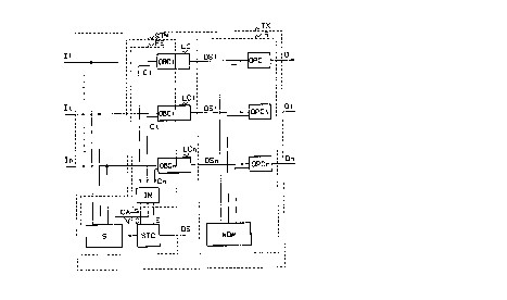
This protection arrangement protects an optical
transmitter device (TX) with n optical transmit circuits
(LCl/LCn) or an optical receiver device (RX) with n optical
receive circuits (RXl/RXn). It includes fault evaluating
means (FE) to detect a defective transmit/receiver circuit
a spare transmit (STC)/receive (SRC) circuit and switching
means (S, Sl) upon detection of a defective
transmitter/receiver circuit by the fault evaluating means
the latter controls the spare circuit and the switching
means which then bypass the defective circuit by the spare
circuit.


French Abstract

Dispositif destiné à protéger un émetteur optique (TX) comportant n circuits d'émission optique (LCl/LCn) ou un récepteur optique (RX) comportant n circuits de réception optique (RXl/RXn). Le dispositif comprend un moyen d'évaluation de défaillance (FE) afin de détecter un circuit émetteur/récepteur défectueux, un circuit émetteur (STC)/récepteur (SRC) de rechange et un moyen de commutation (S, Sl). Lorsque le moyen d'évaluation de défaillance détecte un circuit émetteur/récepteur défectueux, il commande le circuit de rechange et le moyen de commutation, lequel contourne alors le circuit défectueux au moyen du circuit de rechange.

Claims

Note: Claims are shown in the official language in which they were submitted.


THE EMBODIMENTS OF THE INVENTION IN WHICH AN EXCLUSIVE
PROPERTY OR PRIVILEGE IS CLAIMED ARE DEFINED AS FOLLOWS:

1. A protection arrangement for an optical transmitter
device having n optical transmitter circuits whose outputs are
operatively coupled to respective output terminals of the
transmitter device, said protection arrangement including: a spare
optical transmit module operatively connected to inputs of each of
said optical transmitter circuits and having an output on which,
if any one of said optical transmitter circuits is defective, an
optical output signal characteristic of that defective optical
transmitter circuit is produced, said optical output signal
carrying the same information as carried by an input signal
applied to an input of said defective optical transmitter circuit;
and routing means, operatively connected to the outputs of said
optical transmitter circuits and to the output of said spare
transmit module, for providing said optical output signal from
said spare optical transmit module at the respective output
terminal to which the output of said defective optical transmitter
circuit is operatively coupled; wherein said spare optical
transmit module includes: switching means having n inputs
operatively connected to respective inputs of said optical
transmitter circuits, for switching an input signal associated
with said defective optical transmitter circuit to an output of
said switching means; fault evaluating means, operatively
connected to said optical transmitter circuits and having an
output on which a first control signal indicative of said
defective optical transmitter circuit is produced, said first
control signal controlling said switching means so that said
switching means provides at the output thereof said input signal
associated with said defective transmitter circuit; and a spare
transmit circuit which is operatively connected to receive the
output of said switching means and generate said optical output
signal at an output thereof.

2. A protection arrangement according to claim 1 wherein


said routing means comprises: an n port wavelength demultiplexer,
having an input operatively connected to the output of said spare
transmit circuit, and a plurality of outputs; wherein said spare
transmit circuit is tunable and is tuned by a second control
signal produced by said fault evaluating means to produce said
optical output signal with a wavelength characteristic of said
defective optical transmitter circuit; and wherein said routing
means further comprises: n 2-by-1 optical power combiners having
first inputs operatively connected to respective outputs of said n
optical transmitter circuits and having second inputs operatively
connected to respective outputs of said n-ports wavelength
demultiplexer, the outputs of said combiners being said output
terminals of the transmitter device.

3. A protection arrangement according to claim 1 wherein
said routing means includes: n 2-to-1 optical power combiners
having first inputs operatively connected to respective outputs of
said n optical transmitter circuits; and a 1-to-n switch for
switching the output of said spare optical transmit circuit to a
second input of the 2-to-1 optical power combiner operatively
connected to said defective optical transmitter circuit, said 1-
to-n switch being controlled by said first control signal.

4. A protection arrangement according to claim 1, wherein
said routing means includes: n 2-to-1 switches each having a first
input, a second input and an output, the first inputs being
operatively connected to respective optical transmitter circuits;
and a 1-to-n optical splitter for coupling the output of said
spare optical transmit circuit to the second inputs of said n 2-
to-1 switches, each of said n 2-to-1 switches being controlled by
said control signal to switch their output to said second input if
the respective optical transmitter circuit operatively connected
to said first input is defective.

5. A protection arrangement according to claim 1, wherein
said fault evaluating means includes: n test circuits, each being


16


integrally formed as part of a respective one of said optical
transmitter circuits, for testing the operation of said optical
transmitter circuits and for providing respective test result
signals on outputs thereof; and an interpretation module, having n
inputs operatively connected to the respective outputs of said
test circuits, and having an output on which said first control
signal is provided.

6. A protection arrangement according to claim 1, wherein
said fault evaluating means comprises a fault evaluating circuit,
having n inputs and outputs operatively connected to respective
optical transmitter circuits, for testing the operation of said
optical transmitter circuits, and having an output at which said
first control signal is provided.

7. A protection arrangement for an optical receiver device
having n optical receive circuits whose outputs are operatively
coupled to respective ones of n output terminals of said optical
receiver device, said protection arrangement including: a spare
optical receive module, having n inputs operatively coupled to
respective inputs of said optical receiver device, said spare
optical receive module cooperating with said n optical receive
circuits, and having an output at which, if any one of said
optical receive circuits is defective, an electrical signal
characteristic of that defective optical receive circuit is
produced, said electrical signal carrying the same information as
carried by an input signal applied to an input of said defective
optical receive circuit; and routing means, operatively connected
to the outputs of said optical receive circuits and to the output
of said spare optical receive module, for providing said
electrical signal from said spare optical receive module at the
respective output terminal to which the output of said defective
optical receive circuit is operatively connected; wherein said
spare optical receive module includes: switching means, having n
inputs constituting respective input terminals of the receiver
device, n outputs operatively connected to respective inputs of


17


said n optical receive circuits, and a further output for
providing at least said input signal applied to said defective
optical receive circuit; fault evaluating means, operatively
connected to said n optical receive circuits, for producing a
first control signal indicative of said defective optical receive
circuit, said first control signal controlling said routing means;
and a spare receive circuit, operatively connected to the further
output of said switching means, for generating said electrical
signal at an output thereof in response to said input signal
applied to said defective optical receive circuit.

8. A protection arrangement according to claim 7, wherein
said routing means includes n 2-to-1 switches each having an
output operatively connected to a respective one of said output
terminals, each having a first input operatively connected to the
output of a respective one of said optical receive circuits, and
each having a second input operatively connected to the output of
said spare optical receive moduler said n 2-to-1 switches being
controlled by said first control signal.

9. A protection arrangement according to claim 7, wherein
said switching means comprises: n optical splitters each receiving
a respective one of n received input signals, and each having a
first output operatively connected to an input of a respective one
of said optical receive circuits; and an optical power combiner,
having n inputs each of which is operatively connected to a
respective second output of said optical splitters, for producing
at an output thereof, a combination of said n received input
signals; wherein said optical receive circuits are coherent`
optical receive circuits and said spare optical receive circuit is
tunable and is tuned by a second control signal produced by said
fault evaluating means to select from said combination of n
received input signals, said input signal applied to the input of
said defective optical receive circuit.

10. A protection arrangement according to claim 7, wherein


18


said switching means includes: n 1-to-2 switches having respective
first and second outputs, the first outputs being operatively
connected to respective inputs of said optical receive circuits;
and optical coupling means for coupling the second outputs of said
n 1-to-2 switches to the input of said spare optical receive
circuit, said n 1-to-2 switches being controlled by said first
control signal to switch to said second output if the optical
receive circuit operatively connected to said first output is
defective.

11. A protection arrangement according to claim 7, wherein
said fault evaluating means includes: n test circuits, each being
integrally formed as part of a respective one of said optical
receive circuits, for testing the operation of the optical receive
circuits, and for providing corresponding test result signals on
respective outputs thereof; and an interpretation module, having n
inputs operatively connected to respective outputs of said test
circuits, for providing at an output thereof, said first control
signal.

12. A protection arrangement according to claim 7, wherein
said fault evaluating means comprises a fault evaluating circuit
having n inputs and outputs operatively connected to respective
optical receive circuits, for testing the operation of the optical
receive circuits, said fault evaluating circuit providing at an
output thereof, said first control signal.


19

Description

Note: Descriptions are shown in the official language in which they were submitted.


206i~61 8


- 1 - D. MESTDAGH - I. VAN DE VOORDE

PROTECTION ARRANGEMENT FOR AN OPTICAL
TRANSMITTER~RECEIVER DEVICE
The present invention relates to a protection
arrangement for oPtical transmitter and receiver devices.
Such an arrangement is already known in the art.
e.g. from the article "Decreasing survivable fibre network
cost using optical switches" bY Tsong-Ho Wu et al. Globecom
88. IEEE Global Telecommunications Conference and
Exhibition. Hollywood. Florida. November 28-December 1
1~88 Volume l page 3.6.2 second ParagraPh. Therein. a
so-called l:p protection circuit means that p working
circuits are protected by 1 sPare circuit. i.e. when one of
the working circuits is defective it is rePlaced by the
spare one. In this article the protection arrangement
includes a 1:3 electronic Protection circuit and the latter
protects a transmitter~receiver device which consists of
three communication branches each comPrising an oPtical
transmitter and receiver circuit interconnected by an
oPtical cable. The protection circuit includes a
transmitter and a receiver circuit interconnected by an
optical cable. Whenever one of the transmitter circuits or
one of the receiver circuits of the transmitter~receiver
device becomes defective the comPlete communication branch.
i.e. the transmitter circuit. the receiver circuits as
well as the connecting optical cable are bypassed by and
replaced by the protection circuit.
A drawback of this known arrangement is that even
when only either the receiver circuit or the transmitter

~c~ 6
~r
72430-188
circuit is defective, the correctly working transmitter or
receiver circuit as well as the optical cable are replaced
together with the defective circuit.
An object of the present invention is to provide a
protection arrangement of the above type, but which does not
present these drawbacks, i.e. which is more efficient.
According to the invention this object is achieved by
the protection arrangement for an optical transmitter having n
optical transmitter circuits whose outputs are coupled to
respective output terminals, said protection arrangement
including: a spare optical transmit module operatively connected
to inputs of each of said optical transmitter circuits and having
an output on which, if any one of said optical transmitter
circuits is defective, an optical output signal characteristic of
that defective optical transmitter circuit is produced, said
optical output signal carrying the same information as carried by
an input signal applied to an input of said defective optical
transmitter circuit; and routing means, operatively connected to
the outputs of said optical transmitter circuits and to the output
of said spare transmit module, for providing said optical output
signal from said spare optical transmit module at the respective
output terminal to which the output of said defective optical
transmitter circuit is operatively coupled; wherein said spare
optical transmit module includes: switching means having n inputs
operatively connected to respective inputs of said optical
transmitter circuits, for switching an input signal associated
with said defective optical transmitter circuit to an output of
said switching means; fault evaluating means, operatively
connected to said optical transmitter circuits and having an
output on which a first control signal indicative of said
defective optical transmitter circuit is produced, said first
control signal controlling said switching means so that said
switching means provides at the output thereof said input signal
associated with said defective transmitter circuit; and a spare
transmit circuit which is operatively connected to receive the
output of said switching means and generate said optical output


~ G ~

72430-188
signal at an output thereof.
According to the invention this object is also achieved
by the protection arrangement for an optical receiver device
having n optical receive circuits whose outputs are coupled to
respective ones of n output terminals, said protection arrangement
including: a spare optical receive module, having n inputs
operatively coupled to respective inputs of said optical receiver
device, said spare optical receive module cooperating with said n
optical receive circuits, and having an output at which, if any
one of said optical receive circuits is defective, an electrical
signal characteristic of that defective optical receive circuit is
produced, said electrical signal carrying the same information as
carried by an input signal applied to an input of said defective
optical receive circuit; and routing means, operatively connected
to the outputs of said optical receive circuits and to the output
of said spare optical receive module, for providing said
electrical signal from said spare optical receive module at the
respective output terminal to which the output of said defective
optical receive circuit is operatively connected; wherein said
spare optical receive module includes: switching means, having n
inputs constituting respective input terminals of the receiver
device, n outputs operatively connected to respective inputs of
said n optical receive circuits, and a further output for
providing at least said input signal applied to said defective
optical receive circuit; fault evaluating means, operatively
connected to said n optical receive circuits, for producing a
first control signal indicative of said defective optical receive
circuit, said first control signal controlling said routing means;
and a spare receive circuit, operatively connected to the further
output of said switching means, for generating said electrical
signal at an output thereof in response to said input signal
applied to said defective optical receive circuit.
Hence the transmitter circuit as well as the receiver
circuit are protected separately which is more efficient. Indeed,
a defective transmit circuit or a receive line circuit is thus
replaced by the spare optical transmit or receive circuit

-- ~o ~

72430-188
respectively.
The above mentioned and other objects and features of
the invention will become more apparent and the invention itself
will be best understood by referring to the following description
of embodiments taken in conjunction with the accompanying drawings
wherein:
Figs. 1, 5 and 6 show three embodiments of a protection
arrangement for an optical transmitter device according to the
invention;
Fig. 2 represents in more detail the interpretation
module IM of Figs. 1 and 5;
Figs. 3 and 4 respectively represent the circuits D and
P of Fig. 2 in more detail;
Figs. 7 to 9 show embodiments of a protection
arrangement for an optical receiver device according to the
invention.
A definition and a more detailed description of the
optical elements constituting the described embodiments may be
found in general literature concerning the optical field.
Referring to Fig. 1 a l:n protection arrangement for


3a

206~S~8
-


- 4 - D. MESTDAGH - I. VAN DE VOORDE
2-1
an oPtical transmitter device TX is described. This
transmitter device is able to transmit packets of
information for instance from a preceding switch to a
receiver device couPled to a following switch through an
optical fiber link of a switching system (all not shown).
The transmitter device TX has n input terminals
Il~In to which resPective electric signals Il~In are
applied and n outPut terminals Ol~On on which respective
oPtical signals Ol~On are Provided.
TX includes n oPtical transmitter circuits
constituted by n oPtical transmit line circuits LCl~LCn and
associated to a common protection arrangement comprising a
spare optical transmit module STM and a routing circuit R.
The value n which is the number of circuits protected by
the protection arrangement is determined by the mean time
between failure for the transmitter line circuits. the mean
time during which such a circuit is allowed to remain out
of service. the time needed to repair a circuit. the
dimensioning of the switching system etc... A typical
value for n is 16.
The inputs of the n oPtical transmit line circuits
LCl~LCn are constituted by the input terminals Il~In.
These circuits include lasers with resPective fixed
wavelengths ll~ln and produce at their outputs resPective
ones of n optical signals OSl~OSn which are fed to the
routing circuit R and have these fixed wave lengths ll~ln
respectively. Such oPtical transmitter line circuits are
well known in the art and are therefore not described in
m~re detail.
The spare optical transmit module STM comPrises a
switching circuit S. in particular an n-to-1 switch S whose
n inPUts are connected to the inputs of the optical
transmit line circuits LCl~LCn a tunable spare transmit
line circuit STC whose input is connected to the output of
the n-to-l switch S and a fault evaluating circuit FE

2064648
-


- 5 - D. MESTDAGH - I. VAN DE ~OORDE
2-1
controlling the switch S as well as the spare transmit line
circuit STC. Apart from including a tunable laser instead
of a laser with fixed wavelength, the tunable spare
transmit line circuit STC is identical to the optical
transmit line circuits LCl~LCn.
The fault evaluating circuit FE includes n test
circuits OBCl~OBCn which are part of the oPtical transmit
line circuits LCl/LCn respectively. Each of these well
known test circuits OBCl~OBCn transmits so called test
cells to the associated optical transmit line circuit
LCl~LCn to test the status thereof and provides test result
signals Cl~Cn indicative of their status, i.e. working or
defective, a defective circuit being alwaYs PUt out of
service. Each of these test result signals Cl~Cn is a
digital signal having the value 0 when the corresPonding
tested circuit is working correctly, or having the value 1
when this circuit is defective. These signals are applied
to the n inputs of an interPretation module IM which is
also part of the fault evaluating circuit FE. This
interpretation module produces at its output a digital
control signal C and an analog control signal CA indicating
whether one of the oPtical transmit line circuits LCl~LCn
is defective and identifying this defective line circuit.
The digital control signal C is applied to a control input
of the n-to-l switch S and the analog control signal CA
controls the tunable sPare transmit line circuit STC to
which also an enable signal E, additionally provided by the
interpretation module IM, is fed.
rhe interPretatiOn module IM which is represented in
more detail in Fig. 2 comprises a priority circuit P to the
n inPUts of which the n test result signals Cl~Cn are
applied. In response to these test result signals the
circuit P produces at its n outPuts the n signals Dl~Dn
which are applied to n D-latches DLl~DLn constituted by
D-flipfloPs each having an enable port E. These D-latches

20646~8


- 6 - D. MESTDAGH - I. YAN DE VOORDE

provide n output signals 01~0n which are applied to the
inPuts of a decision circuit D and which together
constitute the above mentioned digital control signal C.
The decision circuit D has n additional inputs to which the
signals Cl~Cn are fed and one oUtPUt El connected to the
enable Ports of the D-latches DLl~DLn. The signals 01~0n
are applied to the address inputs of a memory MEM which in
response generates m digital signals CDl~CDm at its output.
These digital signals are converted to the above mentioned
analog control signal CA in a digital-to-analog convertor
D~A. The above test result signals Cl~Cn are additionally
applied to an OR gate which produces at its output the
above mentioned enable signal E.
The priority circuit P makes sure that if several
optical transmit line circuit become defective, i.e. when
several test result signal go high tl), only the signal
with the lowest sequence number is taken into account. For
instance when Cl and C2 are high (1) whereas C3~Cn are low
(0), then Dl is high (1) and D2~Dn are low (0). Such a
circuit can easily be realised bY a person skilled in the
art by means of logic circuitry. One Possible embodiment
is represented in Fig. 4 and its operation is self
explicatorY.
The signals Dl~Dn are latched when the outPUt signal
Z5 El of the decision circuit D ~oes high (1). This circuit
makes sure that its outPUt signal is low - in order to
disable the latches DLl~DLn - as long as one of the line
circuits which was detected to be defective, remains
defecti~e i.e. as long as one of the signals Ol~On and its
corresPonding one of the Cl~Cn signals stay high. Again
such a decision circuit is easy to be designed by a person
skilled in the art by means of logic circuitry. One
possible embodiment is shown in Fig. 3 and is self
exPlicatorY.
Thus the signals Ol~On indicate whether at least one

2Q646~8


- 7 - D. MESTDAGH - I~ VAN DE VOORDE
2-1
of the optical transmit line circuits is defective and
identifies the defective circuit with the lowest sequence
number. Additionally these signals rePresent the address
of a location in the memory MEM where is stored a digital
value indicative of the operating voltage which has to be
applied to the tunable laser of the spare transmit line
circuit STC in case of a defective oPtical transmit line
circuit. More Particularly according to this address the
memory MEM produces at its output an m bit digital code
CDl~CDm indicative of this voltage value. This code
CDl~CDm is read by the digital~analog converter D~A and
converted to the signal CA. The gate OR generates an
enable signal E which is suplied to the spare transmit line
circuit STC (Fig.l) thus enabling the latter circuit only
when one of the optical transmit line circuits LCl~LCn is
defective.
Again referring to Fig. 1 the routing circuit R of
the oPtical transmitter device T comPrises an n-Port
wavelength demultiplexer WDM whose input is connected to
the out~ut of the tunable spare transmit line circuit STC.
and n 2-by-1 oPtical power combiners OPCl~OPCn having a
first inPut connected to the output of the corresponding
optical transmit line circuits LCl~LCn and a second inPut
coupled to a corresponding one of n outPuts of the n-port
wavelength demultiplexer WDM. The outputs of the oPtical
power combiners OPCl~OPCn constitute the output terminals
Ol~On of the oPtical transmitter device TX.
When one of the oPtical transmit line circuits e.g.
~ goes out of ser~ice or is put out of service while
being defective this i 5 indicated by the condition ~high)
of the corresponding test result signal Ci and therefore
also by the condition of the analog control signal CA of
the digital control signal C and of the enable signal E
produced bY the interPretation module IM (Fig. 2) of the
fault evaluating circuit FE. The digital control signal C

- ~064648

-

- 8 - D. MESTDAGH - I. VAN DE VOORDE
2-1
controls the n-to-l switch S in such a way that the latter
connects to its output the one of its inPuts that is
coupled to the defective oPtical transmit line circuit LCi.
As a consequence the input signal Ii is aPPlied to the
inPut of the tunable sPare transmit line circuit STC
enabled by the enable signal E. The analog control signal
CA tunes the laser of the circuit STC, so that it produces
at its output an optical signal OS with wavelength li.
Thus the tunable sPare transmit line circuit STC generates
an oPtical signal OS identical to the signal OSi produced
by the optical transmit line circuit LCi when working
correctly. The n-port wavelength demultiPlexer WDM which
is connected to the optical Power combiners OPCl~OPCn, in
response to the oPtical signal OS with wavelength li being
apPlied to its inPUt, routes this oPtical signal OSi to its
output connected with one of the inputs the optical power
combiner OPCi. Since - as supposed - the defective optical
transmit line circuit LCi connected to the other inPut of
the optical power combiner OPCi is out of service, this
optical power combiner generates at its output the oPtical
signal OS.
The wavelength demultiplexer WDM could be replaced
by a 1-to-n switch controlled by the digital control signal
C to switch the input signal OS to the second input of the
2~ oPtical Power combiner OPCi coupled to the defective line
circuit LCi.
As described above the Protection arrangement is
part of a coherent transmitter device, i.e. one wherein
the transmitted oPtical signals OSl~OSn have different
wavelengths ll~ln. As a consequence the signal OS produced
by the sPare optical transmit module STM when the optical
transmit line circuit LCi is out of service is identical to
the signal OSi to be Produced by that optical transmit line
circuit. This means that it has the same wavelength li and
carries the same information. However, the protection

206~648


- 9 - D. MESTDAGH - I. VAN DE VOORDE
2-1
arrangement is also apPlicable to intensity
modulation~direction detection (IM~DD) systems, i.e.
wherein all signals OSl~OSn have the same wavelength 10.
In this case the signal OS produced by the spare oPtical
transmit module STM is Possibly no longer identical to the
optical signal OSi : it still carries the same information
but may have a different wavelength li, to PassivelY steer
the wavelength demultiPlexer WDM.
Preferably the wavelength li of the optical signal
OS is chosen in the same wavelength window as the
wavelength lo. The reason therefore is related to the
working of the corresponding receiving circuit which
includes an oPtical detector transforming a received
optical signal in an electric one. The optical detector
reacts on optical signals with a wavelength laYing within a
well defined window. If the transmitter would send signals
with a wavelength value outside that window, the optical
detector would have to be tuned accordingly.
The above protection arrangement of Fig. 1 is
2D effective onlY when a defective oPtical transmit line
circuit is out of service or put out of service by the
associated test circuit (not shown).
Fig. 5 represents a second embodiment of a
protection arrangement for an optical transmitter according
to the invention, but which is also effective when the
defective oPtical transmit line circuit is not put out of
service but continues working and Producing faulty output
signals. In this protection arrangement the routing
cjrcujt R comprises a passiYe l-to-n splitter SP, with an
input connected to the outPut of the spare transmit line
circuit STC, and n 2-to-1 oPtical switches Sll~Sln each
having a first signal input connected to the output of a
respective one of the n optical transmit line circuits
LCl~LCn and a second signal input connected to a respective
one of n outputs of the optical sPlitter SP. The oPtical

2064648
-


- 10 - D. MESTDAGH - I. VAN DE VOORDE

switches Sll~Sln further have control inputs which are
controlled by respective bits of the control signal C
(sPlitting of the signal C in its respective bits is not
shown in Fig. 5) in such a way that when one of the optical
transmit line circuits. e.g. LCi. is defective the
corresponding 2-to-1 switch Sli is brought in a condition
wherein its second input is connected to the corresPonding
outPut of the l-to-n oPtical splitter SP. Thus the oPtical
signal OS is transferred to its output. The other switches
Pass to their output the output signal of the oPtical
transmit line circuit they are connected with. In this
waY. even if the defective oPtical transmit line circuit
LCi is still working its output signal OSi is not
transmitted but is replaced by the output signal OS of the
spare transmit line circuit STC. It has to be noted that
the Passive l-to-n sPlitter SP may be replaced by an active
l-to-n switch controlled by the control signal C to reduce
power losses and that in the embodiment just described
there is no need for the sPare transmit line circuit to be
tunable since its output signal is fed to the second input
of each of the 2-to-1 switches Sll~Sln via the l-to-n
splitter SP.
Fig. 6 represents a third embodiment of a protection
arrangement for an oPtical transmitter device. according to
the invention. similar to the one described above in
relation to Fig. 5. but wherein the fault evaluating
circuit FE does not form part of the oPtical transmit line
circuits LCl~LCn. This fault evaluating circuit FE
comprises a controller (not shown) which. just like the
test circuits OBCl~OBCn of Figs 1 and 5. aPplies test cells
to the oPtical transmit line circuits to check the working
thereof. as well as an interpreter module tnot shown) which
according to response cells received from the oPtical
transmit line circuits generates the control signal C and
CA and the enable signal E. These controller and

206~6~8
-


- 11 - D. MESTDAGH - I. VAN DE VOORDE
2-1
interpreter module are similar to the test circuits
OBCl~OBCn and the interpretation module IM of Figs. 1 and
5. However they have obvious additional processor logic
to manage and coordinate the sendin~receiPt of the
test/response cells to~from the n oPtical transmit line
circuits LCl~LCn.
Referring to Fig. 7 a protection arrangement for a
coherent receiver RX is now described. This receiver
device has n inPut terminals Il~In to which respective
optical signals Il~In all having a different wavelength.
are applied and n output terminals Ol~On on which
respective electrical signals Ol~On are provided. R
comprises n coherent oPtical receive circuits RXl~RXn which
are coherent optical receive line circuits. a spare optical
receive module SRM and a routing circuit R.
The input terminals Il~In are connected via the
spare optical receive module SRM to the inputs of
respective coherent optical receive line circuits RXl~RXn
which produce at their outPuts n electrical signals ESl~ESn
that are fed to the routing circuit R. Such line circuits
are well known in the art and are therefore not described
in more detail.
The spare optical receive module SRM comPrises a
switching circuit S. an oPtical amPlifier OA a tunable
spare receive line circuit SRC and a fault evaluating
circuit FE. It has to be noted that the oPtical amplifier
is only needed when the signal received by the spare
receive line circuit is too weak to activate the latter.
~e s~;~ch;ng circuit S includes n l-to-2 optical
splitters SPl~SPn whose inPuts are connected to the
respective input terminals Il~In and the first outputs of
which are coupled to the inputs of the respective coherent
oPtical receive line circuits RXl~RXn. S also includes an
n-to-l optical power combiner OPC whose n inputs are
connected to the second outputs of the oPtical splitters

206~6~8


- 12 - D. MESTDAGH - I. VAN DE VOORDE

SPl~SPn respectively and whose outPut is connected to the
optical amplifier OA.
The fault evaluating circuit FE is similar to the
one described above with respect to the optical transmitter
device T of Fig. 1 and has the same functionalitY. It
includes n test circuits OBCl~OBCn which are part of the
coherent optical receive line circuits RXl~RXn and produce
respective test result signals Cl~Cn indicative of the
status i.e. correctly working or defective of these
coherent optical receive line circuits. FE also includes
an interpretation module IM to the inPUts of which the test
result signals Cl~Cn are applied and which produces at its
outputs a digital control signal C and an analog control
signal CA. These signals both indicate whether one of the
coherent optical receive line circuits RXl~RXn is defective
and also provide the identity of that defective circuit.
The interpretation module IM additionally Provides an
enable signal E which i5 fed to the tunable spare receive
line circuit SRC. The latter is a well known tunable
coherent optical detector which selects the desired
wavelength under control of the analog signal CA and the
enable signal E. Its input is connected to the outPut of
the optical Power combiner OPC through the optical
amPlifier OA.
The routing circuit R comprise n 2-to-1 switches
Sll~Sln each of which has a first input connected to the
outPUt of a respective one of the coherent optical receive
line circuits RXl~RXn and a second inPUt coupled to the
DUtpUt 0~ the tunable spare receive line circuit SRC.
Sll~Sln are controlled by resPective bits of the control
signal C (the sPlitting of C in its different bits is not
shown in Fig. 7) and their outputs are constituted by the
output terminals Ol~On.
When one of the coherent oPtical receive line
circuits. e.g. RXi is defective this is indicated by the

23~648
. ~_

- 13 - D. MESTDAGH - I. VAN DE VOORDE

corresponding test result signal Ci being activated. As a
consequence the circuit IM produces an activated enable
signal E which enables the operation of the tunable oPtical
spare receive circuit SRC and an activated control signal
CA which controls SRC in such a way that the latter
generates at its output an electric digital signal ES which
is applied to the other inputs of all 2-to-1 switches
Sll~Sln. The control signal C controls the 2-to-1 switches
so that Sli connects its second input to its output.
whereas the other switches Sll~Sli-1 and Sli+l~Sln remain
in the position wherein their first input is connected to
their output. In this way the electrical signal ES
produced by the sPare optical receive module SRM is
provided at the oUtPUt Oi of the receiver circuit RX when
the coherent optical receive line circuit RXi is defective.
The other line circuits then provide their normal
electrical signals at the other outputs.
Another embodiment of a protection arrangement. for
an oPtical receiver device according to the invention is
shown in Fig. 8. This embodiment differs from the one
represented in Fig. 7 and described above in that the
switching circuit S is constituted bY n 1-to-2 switches
521~S2n to the inputs of which the input signals Il~In are
applied and by a coupling circuit CM. The switches have
first outPuts connected to respective ones of the n optical
receive line circuits RXl~RXn and second outputs connected
to respective inPUts of the coupling circuit CM. The
latter is constituted bY an n-to-1 optical power combiner
~ whose output i 5 connected to the input of the spare
receive line circuit SRC. These n l-to-2 switches 521~52n
are controlled bY resPective bits of the control signal C
in such a waY that when e.g. the oPtical receive line
circuit RXi is defective. the l-to-2 switch 52i applies its
inPut signal Ii to its second output connected to the spare
receive line circuit via the oPtical Power co~biner OPC

- 206~6q8


- 14 - D. MESTDAGH - I. VAN DE VOORDE

whereas the other switches couPle their input to the input
of the associated oPtical receive line circuits. It has to
be noted that to reduce power losses the passive n-to-l
optical power combiner may be replaced bY an active n-to-l
switch controlled by the control signal C.
Fig. 9 rePresents yet another embodiment of a
protection arrangement for an oPtical receiver device which
i5 similar to the one described above with relation to Fig.
8, but wherein the fault evaluating circuit FE is not Part
of the oPtical receive line circuits RXl~RXn. How this is
realised, i5 already described earlier in connection with
the embodiment shown in Fig. 6.
It has to be noted that an additional advantage of
the different embodiments of the protection arrangement
described above is that they maY use passive optical
elements such as optical power combiners, wavelength
multiplexers~demultiplexers, sPlitters which make the
arrangement more reliable than protection arrangements with
active elements, data format and transmission rate
independent, and immune to electromagnetic noise.
While the principles of the invention have been
described above in connection with specific apparatus, it
is to be clearly understood that this description is made
only bY way of example and not as a limitation on the scoPe
of the invention.

Representative Drawing
A single figure which represents the drawing illustrating the invention.
Administrative Status

For a clearer understanding of the status of the application/patent presented on this page, the site Disclaimer , as well as the definitions for Patent , Administrative Status , Maintenance Fee  and Payment History  should be consulted.

Administrative Status

Title Date
Forecasted Issue Date 1998-04-14
(22) Filed 1992-04-01
(41) Open to Public Inspection 1992-10-03
Examination Requested 1994-11-14
(45) Issued 1998-04-14
Deemed Expired 2003-04-01

Abandonment History

There is no abandonment history.

Payment History

Fee Type Anniversary Year Due Date Amount Paid Paid Date
Application Fee $0.00 1992-04-01
Registration of a document - section 124 $0.00 1992-10-30
Maintenance Fee - Application - New Act 2 1994-04-01 $100.00 1994-03-16
Maintenance Fee - Application - New Act 3 1995-04-03 $100.00 1995-03-15
Maintenance Fee - Application - New Act 4 1996-04-01 $100.00 1996-03-15
Maintenance Fee - Application - New Act 5 1997-04-01 $150.00 1997-03-18
Final Fee $300.00 1997-12-12
Maintenance Fee - Application - New Act 6 1998-04-01 $150.00 1998-03-23
Maintenance Fee - Patent - New Act 7 1999-04-01 $150.00 1999-03-18
Maintenance Fee - Patent - New Act 8 2000-04-03 $150.00 2000-03-13
Maintenance Fee - Patent - New Act 9 2001-04-02 $150.00 2001-03-19
Owners on Record

Note: Records showing the ownership history in alphabetical order.

Current Owners on Record
ALCATEL N.V.
Past Owners on Record
MESTDAGH, DENIS JULIEN GILLES
VAN DE VOORDE, INGRID ZULMA BENOIT
Past Owners that do not appear in the "Owners on Record" listing will appear in other documentation within the application.
Documents

To view selected files, please enter reCAPTCHA code :


To view images, click a link in the Document Description column. To download the documents, select one or more checkboxes in the first column and then click the "Download Selected in PDF format (Zip Archive)" or the "Download Selected as Single PDF" button.

List of published and non-published patent-specific documents on the CPD .

If you have any difficulty accessing content, you can call the Client Service Centre at 1-866-997-1936 or send them an e-mail at CIPO Client Service Centre.


Document
Description 
Date
(yyyy-mm-dd) 
Number of pages   Size of Image (KB) 
Cover Page 1998-04-07 1 47
Cover Page 1994-03-31 1 17
Abstract 1994-03-31 1 18
Claims 1994-03-31 6 207
Drawings 1994-03-31 8 192
Description 1994-03-31 14 535
Description 1996-10-21 15 597
Claims 1996-10-21 5 245
Representative Drawing 1998-04-07 1 9
Assignment 1992-04-01 5 188
Prosecution-Amendment 1994-11-14 12 468
Correspondence 1997-12-12 1 24
Fees 1997-03-18 1 48
Fees 1996-03-15 1 51
Fees 1995-03-15 1 51
Fees 1994-03-16 1 33