Note: Descriptions are shown in the official language in which they were submitted.
206~5~
SPECIFICATION
Title of the InYention
SUBSTRATE FOR MI~ROWAVE (: OMPONENT
Background of the lnvention
Field of ~e inYention
The present inverltion relates to a substra~e for a microwave
component, and more specifically to a microwaYe component substrate
which can be suitably used in fo~ming a microwave component having a
conductor line formed of a compound oxide superconducting thin film
typi~led by a Cu-oxide type compo~nd oxide.
Description of related ~r~
Elec~romagnetic waves called "microw~Yes" or"millimetric waves"
having a wavelen~th in a range of a ~ew tens centimeters to a few
millime~ers can be theoretically said to be merely a part of an
electromagnetic wave spectrum, but have been considered from a
viewpoint of an electric engineer~ng to be a special independent field of
the elec~romagnetic wave, since special and unique methods and devices
have ~een developed for handling these ele~tromagne~ic waves. A
microwave ~ransmission line for guiding the electromagnetic waves in this
band is generally formed of a pair of conductors separateid from each
o~er by a dielectric, one of the pair of conductors bein~ grounded.
On the other hand, in I g86, Bednorz and Muller reported
(La, Ba)2cuo4 showing a superconducting state at a temperature of
3ûK. In 1987, Cllu reported YBa2Cu30y having a superconducting
. ~
- . . . ..
20~ 8~
critical ~emperature on the order of 90 K, and in 1988, Maeda reported a
so-call bismuth (Bi) type compound oxide supercondueting material
having ~ superconducting critical temperature exceeding 100 K. These
compound oxide superconducting materials c~n obt~in a superconducting
with cooling using an inexpensive liquidl nitrogen. As a result, possibi~ity
of actual application of the s~perconduct~r technology has become
discugsed and studied.
l'he compound oxide superconducting material had been, ~t a
beginning, ~ormed as a sintered body by ~ solid phase reaction process,
but have now become possib~e to ~e formed in the form of a thin film,
wi~ advance of technology. In this connection, it has been known that ~he
oxide super~onducting thin fiJm can have an effective superconductin~
characteristics only when it is deposited on a special underlying substrate.
Phenomenon inherent to the superconduction can be advantageously
utilizsd in various applications, and the microwave components are no
exceptions. For examp~e, a micr0strip line has an attenua~ion coef~icien~
that is att~ibuta~le to a resistance component of the conductor. This
attenuation coefficien~ attributable to the resistance component increases
in propor~ioD to a root of a freqllency. On the other hand, the dielectric
loss increases in proportion to increase of the frequency. :Howe~rer, the
loss of a recen~ microstrip line particularly in the range of not greater
than l0GHz is alrnost attributable ~o the resistan~e of the conductor,
since the dieIectric materials have been recently improved. Therefore, if
~he resistance of the conductor in the strip line ~an be reduced, i~ is
possible ~o greatly elevate the perforrnance of the micFostrip line.
As well known, the microstrip iine can be used as a simple signal
transmission ]ine. Hnwever, if a s~litable patte~ning is applied~ the
.
.. ,
'",
,
20~87
microstr~p line can be used as other microwave components including an
inductor, a filter, a resonator, and a delayed line. Therefore,
improYement of the microstrip line will directly result in improvemen~ of
charac~eristics of these microwave ccmponents.
Summary of the Invention
Accordingiy, it is an object of the present invention to provide a
novel microwave component substrate which can be sui~ably used in
folming a microwave component having a conductor line formed of a
compound oxide superconducting thin film typified by a Cu-oxide type
compound oxide.
The above and other objects of the present invention are achieved in
accordance with the present invention by a substrate ~r a microwaYe
component, the substrate being composed of an underlying substrate, and
a ~lrs~ o~cide superconduc~or layer, a dielectric l~yer and a second oxide
superconductor layer stacked on the underlying substrate in the named
order, the die1ectric layer being formed of a cornpound oxide thin film
including La, Ca and Mn and having a perovskite crys~alline s~rocture.
As seen from the above, the substrate in accordance with the present
invention for a microwave component is characterized in that dielectric
layer salldwicAed between a pair of oxide superconducting thin ~llm~
which can constitute a conductnr line, is formed of a thin film of
compound oxide of La, Ca and Mn having ~ perovskite crystallille
structure.
As mentioned hereinbefore, ~he microwave line can be ~ormed of a
pair of conductors sandwiching the dielectric therebetween, and there~ore,
various microwave components can be formed by appropria~ely
, ~ "- ,' ' ` ' :
8 7
pat.ernirlg one or both of ~he pair of conductors. Therefore, if it is
possible to supp]y a substrate cons~ituted of a pair of ~onductor layers and
a dielectric layer therebetween staeked on a whole of a surface of an
underlying substrate, it would become ]possible to simply ~o~n various
microwave components.
On the other hand, the substrate for a microwave component having
a pair o~ oxide superconducting ~hin films as ~ conductor layer can be
obtained by depositing on an underlying substrate a first oxide
superconducting thin film, a dielectric i~yer and a second oxide
superconducting thin film in the named order. However, if an oxide
superconducting thin film is deposited on a usual dielec~ric thin film,
superconducting property nf the deposited oxide superconducting thin
film is remar~cably deteriorated, and ~here~ore, it c~nnot be used as a
superconducting conductor line.
It is known that the compnund oxide of La, Ca and Mn used as the
ma~erial of the dielectric layer in the substr~te in accordance with the
present invention for a microwave component, forms a perovskite
crysta~line structure under a composition ratio of Lao.7ca~ 3Mnl 003~x~
Under dlis compo~ition ratio, the compollnd oxide of La, Ca and Mn ha~ a
lattice con~tant of 3.~7, which is extremely near to the lateice constant
3.82/3.89 of the Y-Ba-Cu type oxide superconductor. In addieion, thi~
compound oxide can be deposited in the ~orm of a thin film having an
excellent suriface smoothness by ~electing arl appropriate deposition
condi~ion. ~herefore, if a Lao.7Ca().~Mnl.l)03 x thin ~ilm is used as an
underlying layer, an oxide superconducting ~hin ~llm of Y-Ba-Cu type
oxide or other oxide superconduclor materials can be crystal-grown with
- 4 -
.. ..
..
. . ~ .
206~g~
a film property which is not inferior to an oxide superconducting thin
fi~n directly deposited on a single crystal underlying substra~e.
In the substrate in accordance with the present invention ~or a
microwave component, since the Lao 7C'ao.3Mnl~0o3-x thin film is used
as the dielectric layer, the second oxide superconducting thin film
deposited on the dielectric layer has a film property m~king it possible to
use ~e second oxide superc~ndu~ting thin fiLm as the conductor line~
In addition, the underlying substrate can be formed of a known
single crystal such as an M~gO single crystal, a SrTiO3 single crystal a
LaA103 single crystal, etc., and the first and second oxide
superconducting thin films can be ~ormed of a Cu-oxide type compound
oxide such as Y type compound oxide, Bi type compound oxide, Tl type
compolmd oxide, etc.
The above and other objects. features and advantages of the present
invention will be apparent from the following description of preferred
examples of the invention with reference to the accompanying drawhlgs.
However, the examp]es explained hereinafter are only for illustration of
the present invention, and therefore, it should be understood that the
present invention is in no way limited to ~he following examples.
Brief Description of the Drawings
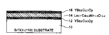
Figure 1 is a diagrammatic sectional view of a microwave
component substrate in accordance with the present invention; and
Figure 2 is a diagrammatic perspectiYe view iliustrating a pattemed
signal conductor of a superconduction microwave resonator formed by
utilizing the microwave component substrate in accordance with the
present invention.
~ . , .
,
8 7
Description of the Pr~ferred embodiments
As shown in Figure 1, a microwave component substrate in
accordance with the present invention was m~anufactllred by using a
SrTiO3 (110) single crystal substrate 10 and an Y-Ba-Cu type compound
oxide (Y:3a2Cu30y (6<y<7)) as an underlying subs~rate and an oxide
superconductor material, and by deposi~ng a first ~xide superconducting
thin film 12, a dielectric layer 14 and a second oxide superconducting thin
film 16 in ~e narned order.
First, the first oxide superconductin~ thin film 12 was formed by
depositing an Y-Ba-Cu type compound oxide thin ~ilm on the underlying
substrate 10 by a magne~ron ~puttering method. The deposition condition
is as follows:
Target : compound oxide sintered body
Y:Ba~ u- 1.0: 2.0: 3.8
(atomic ratio)
Su~strate temperature : 620C
Spu~tering gas : Mixed gas of Ar and O2
(O~/Ar~02) = 0.2 (volurne ratio)
Gas pressure : 20 mTorr
Deposition speed : 10~ ~our
Film thickness : 2000 ~
N~xt, the dielectric layer 14 is formed by dsposi~ing ~n
La~ 7Cao.3Mnl 003 x thin ~ilm on the Y-Ba-Cu type compound oxide
thin film 12 also by a magnetron sputtering methc~d. The depositiort
condition is as f~llows:
Targel : La().7Ca() 3Mnl.oOy
"
.
.
g 7
Subs~rat~ temperature : 629C
Sputtering gas ' Mixed gas of A~r and 2
(02/Ar~0~) = 0.2 (volume ratio)
(~aspressure : 20 mTorr
Deposition speed : '7C 0 ~/hour
Fihn ~ickness : 10 ~m
Then, the second oxide sllperconducting ~in ~llm 16 was fonned by
depositing an Y-Ba-Cu ~ype compound oxide thin film on the
Lao7cao~3Mnl~oo3~x thin film 14 also by a rnagnetron sputterin%
me~od. The deposition condition is the same as that ~or the first oxide
superconducting thin film.
The critical temperature and the critical current densi~y of the
second sxide superconducting ~hin film 16 in ~he microwaYe componerlt
substrate thus formed were measured. The critical temperature was
90 K, and the critical current den3ity at 77 K was S x 10~ A/cm2.
In addition, a microwave resonator was forme~ by using the
microwave component substrate thus formed. As shown in Figure 2, the
second oxide superconducting thin ~ilm of the mi~rowave componen~
subs~rate was patterned by an etching so a~ ~o forrn a cen~er signal
conductor lin~ 1 6A having a width of 20 ~m aIld a length of 20 ~ and a
pair of launching signal conductor lines 16B ~nd l6C haYing a width of
20,um and separated from the ~enter signal conductor line 16A by
10 ,um. Characteristics of the microwave reson~tor were measured at
77 K. For a microwave of 4.5 GHz, the Q factor was 40000~ a~d ~he
transmission loss was 10 dB.
As seen from ~e above, since the microwave eomponent substrate
in accordance with the present invention includes the ~ieleetric layer
,
~ - .
5 ~ 7
composed of a La-Ca-Mn compound oxide, an exeellent superconduc~ing
p~operty of the overlying oxide superconductor is exerted. In addition,
since the microwave component substrate in accordance with the p~sent
invention m~kes it possible to use the microwave component by cool;ng of
liquid nitrogen, utilization of wide and variolls field~ can be expected.
In the above mentioned embodiment, the Cu-oxide type compound
oxide superconductin~g thin film is i~o~ned of the Y-Ba-Cu type compound
oxide superconductin~ material, which is a typical one of a so-called
high-Tc Cu-oxide type supercoilducting material which has been studied
by many researchers since ~he discovery of Bednorz and Miiller in 1986,
and is said to indicate an oxide superconducting ma~erial having a critical
temperature of not less than 30K. There~ore, it could be understood that
the material of the Cu-oxide type compound oxi~e superconducting thin
film is no~ limi~ed to the Y-Ba-Cu ~ype compound oxide superconducting
material, but the Cu-oxide type compound oxide superconducting thin
film can b~ forrned of any other high-Tc Cu-oxide type superconducting
mate~ial including a Bi-Sr-Ca-Cu type compound oxide superconduc~ing
material and a Tl-Ba-Ca-Cu type compound oxide superconducting
material.
The invention has thus been shown and described with re~erence to
the specific embodiments. H~wever, it should be no~ed that the present
inventioll is in no way limited ~o the del~ils of the illustrated structures
but change~ and modifications may be made within the scope of ~he
appended claims.
- 8 -
..
~, :
..;