Note: Descriptions are shown in the official language in which they were submitted.
2066002
JA9-91-515
_
FABRICATION OF QUANTUM DEVICES IN COMPOUND
SEMICO~lOR LAYERS AND RESULTING STRUCTURES
BACKGROUND OF THE INVENTION
Field of the Invention
This invention relates generally to a method for fabricating
semiconductor structures which contain at least a doped
region in a compound semiconductor layer of III-V or II-VI
elements with Group V or Group VI elements introduced
therein, in excess amount, to form either microcrystals or
point defects in the doped region and, more particularly, it
relates to the fabrication of quantum structures in III-V
compound layer such as GaAs. This invention is also
directed ,to the fabrication of an improved FET structure
which has a gate length less than O.l micron.
Description of the Prior Art
Electrons confined in a potential well whose size is
comparable to that of the de Broglie wavelength of an
electron behave quite differently from those in free space.
This special behavior is called the quantum confined effect.
One-dimensional confinement restricts the freedom of
electron motion in a two-dimensional plane. Two-dimensional
confinement allows only one-dimensional motion of carriers:
a structure with this feature is called a quantum wire or
quantum well wire. Three-dimensional confinement does not
allow kinetic motion of electrons, for example, in any
direction. This electronic state is similar to those in
atoms. An electron in this state is called a
zero-dimensional electron and a structure that gives rise to
this state is called a quantum dot or quantum box.
The difference in the dimensionality of these electrons
causes quite a big difference in their density of states and
electronic energy levels. Moreover, a remarkable
improvement can be expected in the performance of devices
that use the feature of electron kinematics in quantum
structures of less than three dimensions. For example, an
2066002
JA9-91-515 2
__
electron s mobility is related to the speed of an electronic
feature of electron kinematics in quantum structures of less
than three-dimensions. For example, an electron s mobility
is related to the speed of an electronic device and its
power consumption. This mobility is subject to electron
scattering processes in semiconductors.
A quantum wire in which an electron has only one-dimensional
freedom of kinetic motion allows only forward and backward
scattering. Only backscattering reduces the mobility, but
the probability of such scattering can be expected to be
very low. Extraordinarily high mobility (107 - 108 sqcm/Vs)
is predicted in the Japanese Journal of Applied Physics,
Vol.l9, No.12, December, 1980, pp.L735-L738 in an article
entitled "Scattering Suppression and High-Mobility Effect of
Size-Quantized Electrons in Ultrafine Semiconductor Wire
Structures" by H. Sakaki. It is easy to understand the
improvement, if we compare this value with that of bulk GaAs
(10 sqcm/Vs).
There have been many attempts to make quantum wires and
quantum boxes, in the hope of effecting a remarkable
improvement in the device performance of electronic devices.
However, these attempts have hitherto resulted only in
rather large quantum wires whose quantum size effect is
insufficient for practical purpose. These quantum wires
also present many problems: a lack of uniformity, low
packing density and difficulty in obtaining a multi-layered
structure and cleanliness in the fabrication process, which
is important for subsequent crystal growth. Even if a
quantum wire has high electron mobility, the current per
quantum wire is so small that a large bundle of quantum
wires is required to operate an actual electron device.
This means that the size uniformity, high packing density,
and multi-layered structure are indispensable for quantum
wires.
Prior methods of fabricating quantum wires can be classified
into four types, as summarized below. Except for molecular
beam epitaxy (MBE), or metal organic chemical vapor
deposition (MO-CVD), described at 4 below, grown quantum
20660~2
JA9-91-515 3
wells or superlattices are used for one-dimensional quantum
confinement. Many different methods are used for additional
confinement.
1. Etching Methods
1) Chemical Etching Method
A preferential chemical etching method used for making
quantum wires was proposed in the Applied Physics Letter
Vol.41 No.7, 1 October, 1982, pp.635-638 in an article
entitled "Toward Quantum Well Wires: Fabrication and Optical
Properties" by P.M. Petroff et al. The surfaces of a (111)
Ga plane of GaAs have strong resistance to the etchant
(H2S04:H202:H20). This characteristic has been used to
obtain a 200~ quantum wire stripe-width from a two-micron
mask pattern. However, this method lacks uniformity of
quantum well size, high packing density structure, and the
ability to process a multi-layered structure. A similar
method was disclosed in the Journal of Crystal Growth 93,
1988, pp.365-369 in an article entitled "Fabrication
Technique for GaInAsP/InP Quantum Wire Structure by
LP-MOVPE" by P. Daste et al for making a GaInAsP quantum
wire which has a 500A quantum wire stripe-width. This
method is, however, subject to the same problems as the
first mentioned approach.
2) Dry Etching Method
K. Kash et al applied a conventional dry etching method to
MBE grown quantum well structures and obtained 400 A + 50 A
quantum wires, as reported in the Applied Physics Letter
Vol.49 No.16, 20 October 1986, pp.1043-1045 in an article
entitled "Optical Spectroscopy of Ultrasmall Structures
etched from quantum wells". A. Scherer et al also made
quantum wires of 300A -400~ stripe-width, as reported in an
article entitled "Fabrication of Small Laterally Patterned
Multiple Quantum Wells" in the Applied Physics Letter Vo.49
No.l9, 10 November 1986, pp.1284-1286. However, these
dimensions are still insufficient to obtain a practical
quantum size effect. In addition, the dry etching process
2066002
JA9-91-515 4
causes damage and contamination to the semiconductor
crystal. The fluctuation of the quantum well size, which
originates from the dry etching resist, is also a problem.
2. Use of a Hetero-Interface or Metal-Oxide-Semiconductor
(MOS) Structure Fabricated on an Edge of a Crystal
The above-mentioned article by Sakaki et al proposed a
conductive wire, that is electrostatically formed by a
positive gate voltage, which induces an n-type inversion
layer on a modified V-groove surface of a p-type quantum
well structure.
This method was extended to a quantum wire fabrication
technique that relies on the MBE overgrowth of a cleaved
multilayer MBE sample with modulation doping. L. Pfeiffer
et al obtained a quantum wire, whose mobilitiy is 4.8 x 10
sqcm/Vs, as reported in an article entitled "Formation of a
High Quality Two-dimentional Electron Gas on Cleaved GaAs",
in the Applied Physics Letter Vol.56, No.17, 23 April, 1990
pp.1697-1699. Although this value is quite high compared
with that of a conventional semiconductor bulk crystal, only
one cleaved facet can be used to make a quantum wire array.
The disadvantage of the fabrication process, which requires
formation on a wafer edge, makes it difficult to fabricate
actual devices.
3. Partial Intermixing of the Micro-Hetero Structure
Impurity-induced disordering is a patternable process for
locally mixing a compound semiconductive micro-hetero
structure without losing its crystal quality. Under
conditions of thermal diffusion or thermal annealing after
ion implantation, impurity ions such as Zn or Si causes
interdiffusion between Ga and Al atoms, which are component
atoms in a III-V compound semiconductor. The intermixing of
atoms forming the quantum structure makes the band gap
larger than that without intermixing.
This intermixing was extended and combined with Ga focused
ion beam implantation to make quantum wires or quantum
2066002
JA9-91-515 5
boxes, as disclosed in Japanese Published Unexamined Patent
Application (PUPA) 61-18192 and Japanese PUPA 62-36886, and
in an article entitled "Optically Detected Carrier
Confinement to One and Zero Dimension in GaAs Quantum Well
Wires and Boxes" by J. Cibert et al in the Applied Physics
Letter Vol.49, No.19, 10 November, 1986. In these prior art
techniques, quantum structures, which are implanted with a
pattern of linear arrays of focused Ga ion beams, change to
linear arrays of mixed crystals, which act as barriers for
linear arrays of quantum wires. Although this method
preserves good crystal quality during the process, the thus
obtained quantum wires or quantum dots have quite vague
patterns in comparison with the original ion implanted
patterns. This results from diffusion, which is the main
cause of intermixing in this system. According to J.
Cibert, there was no apparent formation of quantum wires
when the mask pattern was smaller than 500~. This method is
thus not appropriate process for making good quantum wires.
4. Crystal Growth on a Tilted Substrate
MBE or MO-CVD growth on a (OOl) GaAs substrate mis-oriented
by several degrees from (110) gives direct growth of quantum
wires. The crystal surface of the tilted substrate has many
staircase-like steps with an atomic scale, which can act as
nucleation centers for crystal growth. The crystal growth
of each epitaxy layer starts from these steps.
Alternation between GaAs and AlAs molecular beams gives a
lateral superlattice that is similar to a kind of quantum
wire. The ratio between the GaAs and AlAs stripe-width can
be controlled by the exposure time of each molecular beam.
The size of the stripe-width can be controlled by selecting
the tilted angle of the substrate, but the actual step size
varies broadly. Although this method gives quantum wires
with a stripe-width of lOOA or less and also allows the
integration of multilayers of quantum wire arrays, the well
width fluctuation reduces the advantage of the quantum wire.
M. Tsuchiya et al measured the spectral linewidth of
photoluminescence from quantum wells and quantum wires,
grown by this method at 3.7 meV and 7.7 meV, respectively,
2066002
JA9-91-515 6
-
as reported in an article entitled "Optical Anisotropy in a
Quantum-Well-Wire Array with Two-Dimensional Quantum
Confinement" in the Physical Review Letters, Vol.62, No.4,
23 January, 1989, pp.466-469. This line-width-broadening
mechanism originates from the well-width fluctuation in the
lateral direction of quantum wires.
In summary, all prior art techniques for making ~uantum
wires or quantum dots involve difficulties in either the
well size, the packing density, the direction of the
substrate, or uniformity, thus reducing their effectiveness
for actual usage in electronic devices or optical devices.
SUMMARY OF THE INVENTION
There is disclosed herein a novel fabrication method for
semiconductor structures which allow several advantages over
prior art methods. The use of structures fabricated by this
method in various electronic devices is expected to result
in a greatly enhanced performance.
It is known that epitaxial GaAs films grown at relatively
low substrate temperatures 200 - 250 Centigrade by
molecular beam epitaxy exhibit high resistance and therefore
very favorable insulating characteristics for buffer layers
in metal-semiconductor field effect transistors, as
disclosed in an article entitled "New MBE Buffer Used to
Eliminate Backgating in GaAs MESFET s" by F.W. Smith et al
in the IEEE Electron Device Letters, Vol.9, No.2, February
1988, pp.77-80. A mechanism for the high resistance is
considered to be attributed to the presence of excess
Arsenic ~As) microcrystals imbedded in the GaAs single
crystal layers, as reported in an article entitled "Arsenic
Precipitates and the Semi-insulating Properties of GaAs
Buffer Layers Grown by Low-Temperature Molecular Beam
Epitaxy" by A.C. Warren et al in the Applied Physics Letter
Vol.57 No.13, 24 September 1990, pp.l331-1333 and in another
article entitled "Formation of Arsenic Precipitates in GaAs
Buffer Layers Grown by Molecular Beam Epitaxy at Low
Substrate Temperatures" by M.R. Melloch in the Applied
Physics Letter Vol.57 No.15, 8 October 1990, pp.1531-1533.
2066002
JA9-91-515 7
_
Each As microcrystal acts as a small metal particle, forming
a Schottky barrier at the As/GaAs boundary and thus a
carrier depletion region surrounding the microcrystal.
Consequently, the entire GaAs layer becomes free from
carriers under the condition at which the average As
crystallite distance is close enough to let the depletion
regions overlap each other. For example, the carrier
concentrations that can be depleted have been estimated to
be less than or equal to 2.2 x 10¹⁸/cc for n-type and less
than or equal to 1.6 x 10¹⁸/cc for p-type with the As
microcrystal concentration of 2 x 10¹⁶/cc, assuming the
barrier heights of 0.8 eV and 0.6 eV for electrons and holes
respectively.
The concentration of As microcrystals or point defects in
the form of vacancies or arsenic antesites is controllable
by the MBE growth parameters, such as substrate temperature
and As/Ga flux ratio. A highly resistive GaAs layer thus
prepared shows more favorable insulating features than that
of a Cr doped semi-insulating GaAs substrate, and is
currently considered to be a promising material for device
application. However, a method to permanently recover
electronic conduction in the highly resistive layer has not
yet been found in the prior art techniques.
The present invention provides an approach for recovering
permanently the electronic conduction at an arbitrary area
specified by the implantation of appropriate amounts of
group III elements, that is, Ga ions, in the highly
resistive layers which may be doped or undoped. At the area
of implantation, the As microcrystals change into a GaAs
single crystal phase through the reaction Ga + As ~GaAs
after an appropriate annealing step, resulting in the
elimination of carrier depleted regions. This makes it
possible to generate and confine carriers inside of the
implanted regions in doped but highly resistive target GaAs
layers which contain excess As microcrystals or point
defects.
Co-implantation of ions of Group III elements and Group II
elements provides semiconductor single crystal regions which
2066002
JA9-91-515 8
have holes, and co-implantation of ions of Group III
elements and Group IV elements provide a region with
electrons as carriers after an appropriate annealing step.
This makes it possible to generate and confine both p- and
n-type carriers inside of the implanted regions even if the
target III-V semiconductor layer is undoped. Use of this
technique can provide devices such as GaAs short channel
devices which have high-speed performance and which can be
integrated in both lateral and vertical directions. At this
point, it should be appreciated, that while GaAs has been
discussed by way of example, other compound semiconductors
such as semiconductors, made from the II-VI elements may
also be utilized. In addition, binary, ternary and
quaternary compounds of both III-V and II-VI elements may be
used in the practice of the present invention.
BRIEF DESCRIPTION OF THE DRAWINGS
FIGS. lA through lC show fabrication process of GaAs wires.
FIG. 2 is a top view of a wire structure with electrical
contacts.
FIG. 3 is a cross section view of contact region.
FIG. 4 is an illustration of depletion region caused by
Arsenic microcrystal and quantum wire fabricated therein.
FIG. 5 shows fabrication process for stacked GaAs wires
structure.
FIG. 6 is a side view of a stacked wire structure with side
contacts.
FIG. 7 is a top view of Ga implanted regions in forms of
dots.
FIGS. 8A through 8E show fabrication process of short
channel GaAs FET.
2066002
JA9-91-515 9
FIGS. 9A and 9B show alternative fabrication process of
short channel GaAs FET.
FIG. 10 is a graph showing a transient response of electron
drift velocity in Si.
FIGS. 11 and 12 are graphs showing a transient response of
electron drift velocity in GaAs.
FIGS. 13A and 13B show fabrication process of short channel
GaAs FET for normally-off and on devices.
FIG. 14 is a cross section view of multi-layered integrated
circuits.
DESCRIPTION OF THE PREFERRED EMBODIMENT
Throughout the following description, the same reference
numbers refer to the same elements in all the figures.
Example 1 - Quantum Wires -
The first example is the fabrication of quantum wires, which
is schematically illustrated in FIGS. lA - FIG. lC. A
l-micron thick, highly resistive GaAs (doped with Si = 1 x
10 7/cc) layer 2 is first grown on a semi-insulating GaAs
(100) substrate 1 by molecular beam epitaxy (MBE) at a
substrate temperature of 200 Centigrade with As4/Ga flux
ratio of less than 16, as illustrated in FIG. lA. The
growth rate is 1 micron/hr. The estimated concentration of
As microcrystals in bulk layer 2 is 10 - 10 7 atoms/cc. A
microcrystal, typically a 50A cluster, consists of 2 x 10³.
As atoms on average. The sample is then transferred through
ultrahigh vacuum transfer modules to a focused ion beam
(FIB) chamber for the Ga writing from which quantum wires
are ultimately formed. The Ga writing is performed by using
a Ga focused ion beam having a beam diameter of 0.25 micron
to form an array of straight Ga regions 3. The array may
consist of 100 such regions 3. The dose is 1014 Ga /sqcm.
The acceleration voltage and beam current are 150keV and
lOOpA, respectively, so that the ion-implantation depth is
2066002
JA9-91-515 10
0.15 micron. The concentration of implanted Ga is 2 x 10
2 x 10² atoms/cc. A cross-sectional view of such
Ga-implanted region is shown as region 3 in FIG. lB. A top
view of the array of Ga regions 3 can also be seen in FIG.
2. The length of each Ga-implanted region 3 is 50 microns,
and the spacing between two consecutive regions 3 is 0.1
micron.
After the Ga writing is completed, the sample is transferred
back to the MBE growth chamber where a second low
temperature GaAs layer 4 (FIG. lC) of 0.1 micron thickness
is grown on top of the layer 2 at the same growth conditions
as specified for the growth of layer 2. Note, however, that
the layer 4 is intentionally undoped. This is followed by
the growth of a 1.5 micron thick undoped GaAs cap layer 5
(FIG.lC). This step is performed at a substrate temperature
of 580-600 Centigrade.
Finally, the sample is again transferred to the FIB chamber,
and Si and Ga ions are co-implanted in a pattern 6 at both
ends of the array of regions 3 as shown in FIG. 2. The
alignment between the array of regions 3 and pattern 6
viewed from the sample surface is also shown in FIG. 2.
Note that the array of regions 3 is embedded in highly
resistive GaAs as shown in FIG. lC, which corresponds to a
cross section A-A in FIG. 2. The implantation depth has to
be deep (about 0.2 micron) enough to reach the embedded
array of regions 3. A cross section of the implanted region
B-B is also shown in FIG. 3 for comparison. The purpose of
this process is to establish electrical contact from the top
surface to the array of regions 3, so the beam size can be
rather large (about l micron) compared to the previous Ga
writing process. The co-implantation step is followed by
either laser flash annealing or other rapid thermal
annealing step to recover the crystal quality of regions 3
and co-implanted regions 6, and then by the formation of
n-type ohmic contact pads 7 (FIG. 3) on top of regions 6.
After annealing, regions 3 and 6 have been recoverd or
converted to conductive regions of GaAs in the form of
~uantum wires. The steps involved in the electrical contact
2066002
JA9-91-515 11
fabrication are similar to those used in conventional
semiconductor device processing.
The resulting structure is then subjected to transport
measurements to determine its characteristics. Finite
conductance ~2 x 10 mho) is observed together with
characteristic magnetotransport behavior, both indicative of
the presence of electrons in the recovered GaAs wires. An
effective wire diameter is estimated to be about 30nm,
taking account of a depletion region which extends from
outside to inside of the GaAs wires. 30nm is sufficiently
less than the de Broglie wavelength of electrons or holes to
permit the quantum size effects such as high electron
mobility.
The formation mechanism of quantum wires in highly resistive
GaAs can be understood by considering FIG. 4. Note that
FIG. 4 is an enlargement of the tube-like shape of
ion-implanted regions 3 and As microcrystals 8 after GaAs
layer 4 is grown. The solid state reaction Ga + As ~GaAs
occurs in the regions 3 where Ga ions are implanted in a
concentration of As microcrystals 8 so as to return regions
3 to stoichiometry. This results in the appearance of a
specific region 9 which is undepleted as compared with
depleted region 10. Thus, carriers which are electrons for
Si-doped GaAs are confined in region 9. Annealing effects
during the cap layer growth (at 580-600 Centigrade) and
after the second ion implantation also promote reactions for
GaAs formation and recrystallization which results in
conductive regions 9.
Note that the width or diameter of a region 3 is determined
by not only the ion beam diameter but also by the extension
of the depletion regions 10 from the surrounding As
microcrystals 8. The latter is determined by the
concentration of microcrystals 8 which is controllable by
the substrate temperature, the As4/Ga flux ratio during the
MBE-growth step and the silicon concentration. Similarly,
the wire depth, or the size in a vertical direction of FIG.
4 is determined by the ion-implantation depth and the above
MBE parameters. The former is controlled by
JA9-91-515 12 2 0 6 6 0 ~ 2
ion-implantation parameters such as beam acceleration
voltage and current.
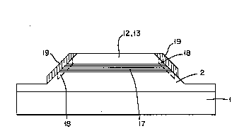
Example 2 - Stack of Wire Arrays -
The second example of wire arrays is schematically
illustrated as an end view in FIG. 5. The first row of the
array of Ga wires 3 is fabricated in the same fashion as
described in example 1. A second GaAs layer 11 is then
grown on top of layer 2, embedding first row of wires 3
underneath it, followed by the successive fabrication of a
second row of Ga wires 3 on top of layer 11. Layer 11 is
grown under the same growth condition as layer 2. The
fabrication process of Ga wires 3 is repeated six times in
total forming structure 17, and then, undoped low
temperature (200 Centigrade) and high temperature (600
Centigrade) GaAs cap layers 12 and 13 are grown on top of
layers of wires 3. The quantum wire structure 17 composed
of six rows of GaAs wires 3 prepared as above, is shown in
FIG. 6 as a side view of FIG. 5. In this case, the
electrical contact is achieved by side wall contacts 19 in a
mesa structure fabricated by conventional lithography
techniques. An edge of the top of the mesa is aligned
perpendicular to the axis of wires 3. The contact formation
is done at the mesa edges 18 (FIG. 6) by co-implantation of
Ga and Si ions by FIB, followed by rapid thermal annealing
and n-type metallurgy 19. Magnetotransport behavior through
two contact probes shows the existence of electrons confined
in the GaAs wires 3, and, thus, confirms the formation of
quantum wires.
Example 3 - Quantum Dots -
An array of Ga dots 20 is fabricated in a low temperature
grown GaAs layer 21, as seen on the top view of the sample
surface of layer 27 (FIG. 7). Ga ions are implanted in the
form of an array of dots each with a diameter of 0.2 micron.
Repetition of the growth and dot fabrication process like
Example 2 yields a stack of arrays of dots (15,000 dots).
After an annealing step, the sample is evaluated by infrared
reflection spectroscopy in which reflectance modulation is
206G002
JA9-91-515 13
observed at the photon energies corresponding to those of
confined states in a quantum dot of about 30nm diameter.
Such a structure can transform electromagnetic waves from
one frequency to another and also act as a polarizer.
Example 4 - p-type Wires -
An array of Ga wires 3 is fabricated in a same way as
described in connection with Example 1. The host GaAs layer
(layer 2 in FIG. 1) in this case, however, is intentionally
doped with an acceptor impurity Be. The GaAs layer is grown
by MBE at the substrate temperature 200-250 Centigrade with
As4/Ga flux ratio of less than 16; the same as the GaAs
layer 2 in Example 1. In the electrical contact process,
Be ions are used instead of Si ions because of the p-type
contacts. A conductance of about 10 5 mho/100 wires is
observed together with characteristic magnetotransport
behavior indicative of the carrier confinement.
The resulting quantum wire and dot structures have a wide
range of application. For example, p- or n-type wires are
used for channel regions for ultrasmall and fast FETs which
are smaller than FETs described below in Examples 5 to 8. A
quantum dot array may be used as a micro switching device,
as described in Scientific American, March, 1988, pp.96 to
100, in an article entitled "The Quantum-Effect Device:
Tomorrow's Transistor" by R. T. Bate.
Example 5 - Short Channel FETs -
The fifth example shows the fabrication of a short channel
GaAs FET, which is schematically illustrated in FIGS. 8A -
8E. A 1-micron thick, highly resistive GaAs (Si=1 x
1017/cc) layer 22 is first grown on a semi-insulating GaAs
(100) substrate 21 by molecular beam epitaxy (MBE) at the
substrate temperature of 200 Centigrade with As4/Ga flux
ratio less than 16, as illustrated in FIG. 8A. The growth
rate is 1 micron/hr. The estimated concentration of As
microcrystal in layer 2 is 10 6 _ 1ol7 atoms/cc. The sample
is then transferred through ultrahigh vacuum transfer
modules to a focused ion beam (FIB) chamber for the Ga
2066002
JA9-91-515 14
-
pattern writing. Pattern 23 (which may be rectangular) is
written by using a Ga focused ion beam of a beam diameter
of 0.25 micron to form an n-type region. The dose is 1 x
1014 Ga /sqcm. The concentration of the implanted Ga is
- 10 atoms/cc. A cross-sectional view of such
Ga-implanted region 23 is shown in FIG. 8B. The length of
region 23, indicated as L1 in FIG. 8B, is 5 microns and the
implantation depth, indicated as D1, is 150 nm (0.15
micron). The remaining dimension of region 23 is 50 micron.
In a subsequent step, writing of rectangular pattern 24 is
carried out by using a Ga and Si focused ion beam of a
beam diameter 0.25 micron to form n type source and drain
regions. In this FIB process, the density of Si is
controlled to obtain a constant value (Si=1018 atoms/cc) for
the region 24. The density of implanted Ga is also
controlled to obtain a constant value of (Ga=2 x 10¹⁹ - 2 x
1o20 atoms/cc) for the region 24. The achieved
ion-implantation depth, indicated as D2, is 250 nm. The
remaining portion of region 23 shown as n-type region 26
between two regions 24 becomes channel for the FET as shown
in FIG. 8C. The effective n-type channel length of region
26, indicated as L2 in FIG. 8C, is 0.09 micron.
After the writing is compLeted, the sample is transferred
back to the MBE growth chamber where a second low
temperature GaAs layer 27 (FIG. 8C) of 0.1 micron thickness
is grown on top of the layer 22 under the same growth
conditions as layer 22. Note, however, that the layer 27 is
intentionally undoped.
Finally, the sample is again transferred to the FIB chamber,
and Si and Ga ions are co-implanted in pattern 28 at both
ends of n region 24 as shown in FIG. 8D. Be and Ga ions
are co-implanted to form gate region 29, which has a 0.05
micron effective gate length.
The implantation depth has to be deep enough (about 0.11
micron) to reach the embedded regions 24 and 26. This is
followed by either laser flash annealing or other rapid
thermal annealing techniques to recover the crystal quality
of the implanted regions 24 and 26 and n-type ohmic contact
2066002
JA9~91-515 15
-
pads 28 and p-type gate 29 on top of the region 27. Thus,
the channel, source, drain and gate regions are fabricated
using a maskless FIB technique.
The subsequent processes involved in the electrical contact
fabrication are similar to those used in a conventional
semiconductor device fabrication process. In FIG. 8E, ohmic
electrodes 31 for n-type regions 28 are made of Au/Ge/Ni and
contact 32 made of p-type WNX to gate 29 are deposited
through holes in insulating layer 30. Thus, the obtained
FET has a planar structure suitable for various kinds of
subsequent processes.
The annealing step should be performed before ohmic
electrodes 31, 32 are fabricated. Preferably the annealing
should be done after insulating layer 30 is formed over
layer 27, but it can be done before layer 30 is formed if it
is carried out in an arsenic atmosphere.
The fabrication steps shown in FIGS. 8B and 8C have an
alternative as shown in FIGS. 9A and 9B. In this
alternative process, n-type region 23a is first formed in
GaAs layer 22. Region 23a is formed in a same manner as
region 23 except that the length L1 is 0.09 micron (FIG.
9A). Then regions 24 are formed on both sides of the region
23a (FIG. 9B).
Formation of the short channel GaAs FET is attributable to
the solid reaction Ga + As ~GaAs occurring in the regions
23, 24, 28 and 29 where Ga ions are implanted in such
concentration that the As microcrystals are converted to
crystalline GaAs.
The resulting normally-off, junction FET is characterized by
current-voltage measurements for various gate biases. The
transconductance 1.2S/mm is observed without hysterisis in
its I-V characteristics.
The performance of an FET fabricated according to the
above-mentioned steps is explained below. In electronic
devices, a drift velocity of carriers under electric field
JA9-91-515 16 2066002
has significant meaning to determine the device performance,
especially its speed and power consumption. The drift
velocity in semiconductors depends on the electronic
structures of the channel which transports the carriers.
FIG. 10 shows a transient response of electron drift
velocity of n-type silicon obtained by the Monte Carlo
method. A similar transient response for n-type GaAs is
shown in FIG. 11.
From these figures it should be clear that GaAs electronic
devices can be expected to have switching speeds on the
order of half a picosecond. If the transit time of
electrons exceeds several picoseconds, the relationship
shown in FIG. 11 need not be used. Alternatively, FIG. 11
may be recast as FIG. 12 which shows the electron drift
velocity change along the channel distance which is obtained
by using the Monte Carlo technique.
The shortest channel length in FET devices is 0.1 micron in
Si metal-oxide-semiconductor (MOS) FET structures as
reported by G.A. Sai-Halasz in an article entitled
"Experimental Technology and Performance of 0.1 micron
Gate-Length Low Temperature Operation MOSFETs", in the
Extended Abstracts of the 20th Conference on Solid State
Devices and Materials, Tokyo, 1988, pp.5-8. This extremely
short channel was obtained not in GaAs but in silicon. This
indicates that for the same channel length, higher switching
speed can be obtained in GaAs.
In GaAs devices, such as metal-semiconductor (MES) FET, a
more complicated fabrication process is required, even for
0.5 micron length, compared to Si MOS-FET technology, as
described by K. Ishida et al in an article entitled "A 5
Gb/s 4 Bit Shift Register with 0.5 micron WNx-gate GaAs
MESFETs", in the Extended Abstracts of the 20th Conference
on Solid State Devices and Materials, Tokyo, 1988,
pp.129-132. In the case of GaAs, high speed, reliable
device was not achieved by the prior art techniques because
(1) the short channel effect could not be fully utilized and
(2) punch-through effects could not be prevented.
20660~2
JA9-91-515 17
In contrast, the GaAs device obtained by the above-mentioned
method has a very short channel and thus has high-speed
performance. High resistivity layer 22 prevents
punch-through effects from which the conventional GaAs FETs
with short gate length suffered. In addition, a gate region
less than 0.1 micron in length can be fabricated easily
using a maskless FIB technique.
Example 6 - Normally-On and Off Type FETs -
The sixth example of short channel FETs are schematically
illustrated in FIGS.13A and 13B. The n-type region 33 for a
normally-off FET is fabricated in the same fashion as
described in Example 5, and the n-type region 34 for a
normally-on FET is fabricated by increasing both the beam
acceleration voltage and current. The depth of region 33 is
150 nm and that of region 34 is 250 nm. The following
fabrication process is the same as that described in
connection with Example 5. Source and drain regions 35 are
formed in a similar way for normally-on and normally-off
FETs. An integrated circuit is obtained with this
normally-off and on FET combination. The advantage specific
to this example is that the source, drain and channel
regions for both normally-on FET and a normally off FET is
that they are fabricated on the as-formed surface of a GaAs
crystal layer, as shown in FIG. 13.
Example 7 - Three-Dimensional Integration of Short Channel
FETs -
The three dimensional integration, in both lateral andvertical directions, of short channel FETs is schematically
shown in FIG. 14. GaAs layer 37 is formed under the same
conditions as layer 22 of Example 5 and is intentionally
undoped. The first level of an n-type active region 38 for
an n-FET and a p-type active region 39 for a p-FET are
fabricated in the same fashion as described in Example 5.
Here, active region means the source, drain and channel of
the FET. For an n-type active region, the channel region is
fabricated by co-implantation of Ga and Si and source and
drain regions in a similar way except that the Si ion dose
2066002
JA9-91-515 18
is increased. For p-type region 39, the only alteration is
that Si is substituted for the Be ion. The second
undoped-GaAs layer 40 is then grown on top of layer 37,
embedding the active regions 38 and 39. Layer 40 is grown
under the same growth condition as layer 27 in Example 5.
The structure is transferred to the FIB chamber and a p-type
gate region 41 and n-type gate region 42 are made in a
manner similar to that shown in Example 5. Then, the third
undoped-GaAs layer 43 is grown under the same conditions as
layer 37. The second level of an n-type active region 47
for an n-FET and a p-type active region 46 for a p-FET are
fabricated in the same way as for regions 38, 39. The
contact region 44, which connects between gate region 42 and
n-type active region 47, and region 45 which has opposite
conductivity to that of region 44 are made by
co-implantation of Ga and Si ions or Ga and Be ions.
This process is repeated for making undoped-GaAs layers 48,
51 and 56 and making n-type gate regions 49 and 59, p-type
gate regions 50 and 57, n-type active region 55 and contacts
53 and 58, and p-type active region 54 and contacts 52 and
60. Electrical contacts 61 to 64 are formed through
insulating layer 65 in the same manner as described in
connection with Example 5.
The method described here can be repeatable for many more
levels if it is required. In such integrated circuits, the
size of each FET is quite small compared to FETs in
conventional integrated circuits, because many bonding pads,
which have 100 micron square areas, can be extremely reduced
by adopting the three dimensional internal connections
described above which may only be 1 micron square in area.
In three dimensional structures, low-power consumption is
indispensable because it is very difficult to obtain good
heat sinking in such structures. In this connection,
another benefit of this structure is the low-power
consumption of complimentary FET circuits. In this
fabrication method, to obtain n- and p-type channels is
2066002
JA9-91-515 19
_,
quite simple; just change the source of ions to be
implanted.
As mentioned in the above three examples, this invention
provides a practical method for fabrication of short-channel
FETs, of the normally-on and off varieties as well as
complimentary FET circuits.
As also mentioned in the above examples, this invention
provides a practical method for fabrication of micro
structures such as quantum wire and dot structures and FETs
of less than O.l micron gate length. Besides GaAs, similar
effects are expected to occur in other III-V compound
semiconductors and alloys, such as GaAlAs, (In,Ga)As and
InP. For example, implantation of In ions also results in
the elimination of As or P microcrystals and the consequent
recovery of the original III-V compound.
While III-V compounds have been utilized herein to fabricate
the various structures shown, it should be appreciated that
other compound semiconductors such as II-VI compounds and
their usual dopants may also be used in the practice of the
present invention. For example, ZnSe containing Se
microcrystals and/or point defects (doped with Al for n-type
and N for p-type) may be implanted with Zn in specific
regions to reform ZnSe upon annealing as an electronically
active region. Other combinations including ternary and
quaternary II-VI compounds will easily come to the minds of
those skilled in the semiconductor arts.
In the above exposition, it should be noted that in most
instances, it is the presence of excess amounts of the
anionic component of a doped or undoped compound
semiconductor which results in the formation of
microcrystals and/or defects and that the cationic component
of the compound semiconductor, in most instances, is ion
implanted to compensate for the presence of the anionic
microcrystals and/or defects. These components are then
annealed to reform the original compound semiconductor.
However, in some instances, either the anion or the cation
may appear as the microcrystal and/or defect by depositing
2066002
JA9-91-515 20
.~
the compound semiconductor with an excess of either ion. In
this instance, the element not in excess in the deposited
layer would be implanted and annealed to reform the compound
semiconductor. Cadmium Telluride is one such compound
semiconductor material.
In connection with the formation of layers of high
resistivity, the terms microcrystals and point defects have
been used when one of the elements of a compound
semiconductor appears in excess in a deposited layer of
compound semiconductor. To the extent that microcrystals
and point defects appear to differ only in the number of
atoms of a particular atomic species with microcrystals
having a much greater number of atoms, both of these
entities may be characterized as clusters of atoms. Thus,
as claimed hereinbelow, the terms "clusters of atoms" or
"clusters of one of the compound semiconductor elements" are
intended to cover both microcrystals and point defects.