Note: Descriptions are shown in the official language in which they were submitted.
CFO 8402 ~C~
-- 1 --
l APPARATUS FOR RECORDING AND/OR
REPRODUCING INFORMATION
BACKGROUND OF THE INVENTION
Field of the Invention
This invention relates to an apparatus such
as a memory apparatus for effecting super-high density
information recording (erasing) and/or reproduction
by the use, for example, of a tunnel current.
Related Background Art
Semiconductor memories and magnetic memories
using a magnetic material or a semiconductor as a
material have heretofore been the mainstream, but in
recent years, with the advancement of the laser
technique, inexpensive and highly dense recording mediums
using optical memories using organic thin film of
organic coloring matters, photopolymer or the like
have made their advent.
On the other hand, recently, a sc~nn;n~ type
tunnel microscope ~hereinafter abbreviated as STM)
through which the electron structure of the surface
atom of a conductor can be directly observed has been
developed [G. Binning et al., Phys. Rev. Lett., 49,
57 11982)] and measurement of high resolving power
of a real spatial image has become possible irrespective
of single crystal or an amorphous material, and STM
has the advantage that it can observe with low electric
-- 2
1 power without imparting any damage by a current to
a sample and further~ can operate even in the atmosphere
and can be used for various materials and therefore,
wide applicakions thereof are expected.
The STM utilizes the fact that ~hen a voltage
is applied between a metallic probe ~probe electrode)
and an electrically conductive substance and the probe
is brought close to the substance to a distance of
the order of 1 nmr a tunnel current flows. This current
is very sensitive to any variatlon in the distance
between the two. By scanning the probe so as to keep
the tunnel current constant, various kinds of information
regarding all electron clouds in the real space can
also be read. In this case, the resolving power in
the in-plane direction is of the order of 0.1 nm.
Accordingly, if the principle of the STM is
applied, it will be possible to effect high-density
recording and reproduction sufficiently at the atom
order (sub-namometer). For example, in the recording-
reproducing apparatus disclosed in Japanese Laid-Open
Patent Application No. 61-80536, atomic particles
adhering to the surface of a medium are removed by
an electron beam or the like to thereby effect writing,
and this data is reproduced by an STM.
A method of effecting recording and reproduction
in an STM by the use of a thin film layer of a material
having a memory effect for the switching characteristic
1 of a voltage or a current, for example, ~ electron
line organic compound or a chalcogen compound, as a
recording layer is disclosed in Japanese Laid-Open
Patent Application No. 63-161552, Japanese Laid-Open
Patent Application No. 63-151553, etc. According to
this method, if the bit size of recording is 10 nm,
recording and reproduction of a capacity as great as
1012 bit/cm2 is possible.
To effect recording or reproduction on a memory
medium in an actual apparatus, it is necessary to
maintain and stabilize the spacing between the recording
layer and the probe electrode at a distance over which
a tunnel current flows. So, heretofore, the control
of the spacing has been effected so
that the average spacing between the recording layer
and the probe electrode may assume a predetermined
value, that is, the average value of the tunnel current
may be a predetermined value. This is disclosed, for
example, in Japanese Laid Open Patent Application No.
1-133239. This method is such that servo control is
applied so as to fix and maintain the probe electrode
near the average position of vertical movement so that
the probe electrode may'not vertically move without
omission in conformity with the value of the recording
bit.
Also, when the tunnel current is to be inten-
sified to write information onto the recording layer,
7~'
1 the hold control of an actuator ~hereinafter referred
to as the pre-value hold) has been effected so as to
hold the position in Z di.rection at a predetermined
value so that the spacing between the probe electrode
and the recording layer may not be greatly varied by
a great current then flowing.
Eowever, the system which effects the control
of the spacing between the probe electrode and the
recording layer by the use of the average value of
the tunnel current suffers from the following three
problems:
(1) When the scanning speed of the probe
electrode is increased, the tip end portion of the
probe electrQde may collide with the convex recording
bit of the recordins layer. Particularly when the
shape of the recording bits is not uniform, the pos-
sibility of the collision occurring frequently becomes
high.
What determines the spacing between the prabe
electrode and the recording laye~r is the average value
of the tunnel currents flowing in the ON state and
the OFF state, respectively. This average value is
determined chiefly by the tunnel current when the
recording layer is in the ON state. The ON state is
the state of the convexly shaped bits in a case where
recording is effected by the modulation of the surface
shape, and is a state in which the electron density
~ O ~ 7 7
1 is high and the electrical conductivity with respect
to the base electrode has become high in the case
of the recording in the modulation of the e]ectron
state (the electrical conductivity state) Therefore,
the spacing between the probe electrode and the record-
ing layer is affected by the pattern of data rows
written on the recording layer, i.e., the detection
frequency of the ON state bits.
The tunnel current is controlled by the very
minute spacing (usually 1 nm or less) hetween the probe
electrode and the recording layer and therefore, even
if use i5 made of a modulation system which does not
have a direct current component such as EFM, any slight
variation in the average tunnel current by the differ-
ence in substance between data being recorded willresult in the collision with the probe electrode at
the ON state bit.
Also, from the necessity of reading out data
at a high speed, the cutoff frequency of a low-pass filter
is set to a sufficiently low value as compared with
the signal band frequency of recorded data. However, if the
cutoff frequency of the low-pass filter is set to a low
value, the probe electrode will not be able to be
retracted at a high speed and may collide with the
recording layer when a greatly convexly shaped ON state
bit by the irregularity of writing during recording
is detected.
2~66 ,L~s77
1 When the probe electrode collides with the
recording layer, not only recorded data are lost but
also the probe electrode may be unrecoverably damaged,
and the above-noted problem will remarkably reduce
the reliability of an information reproducing apparatus
utilizing a tunnel current.
(2) If during data writing, the spacing between
the probe electrode and the recording layer is pre-
value~held and controlled, there may occur irregularity
in the shape of written bits. Particularly, in the
first bit writing of data rows, the possibility of
the contact of the probe electrode with the recording
layer shape-modulated by a writing cuxrent occurring
frequently is high.
The states of an example of the prior art during
recording are shown in Figures 6, 7 and 8 of the
accompanying dLawings. Figure 6 shows the state before
the application of a writing pulse voltage, and Figure
7 shows the state after the application of the writing
pulse voltage, i.e.j a state in which the surface of
the recording layer is melted and expanded by energy
poured from the pulse voltage into the recording layer
and convexly shaped recording is accomplished rightly.
However, this recording method has a very
unstable factor. When an electric current is caused
to flow from the probe electrode to the recording layer
to thereby melt the recording layer, the recording
2~i .L~7~
l layer begins to expand. At this time, the spacing
between the probe electrode and the recording layer
becomes smaller by the amount of expansion of the
recording layer. This reduction in the spacing
increases the electric current flowing between the
probe electrode and the recording layer. This increased
electric current further expedites the melting of the
recording layer to thereby further expand the recording
layer toward the probe electrode. As a result, as
shown in Figure ~, the recording layer collides with
the probe electrode and an extremely large recording
hit is formed. ~he formation of such recording bits
irregular in size not only reduces the S/N ratio of
the signal, but also causes the collision of the probe
electrode during the aforedescribed reproduction.
A similar problem has arisen when recording
is effected with the electron state of the surface
of the recording layer modulated. When the electron
state of the surface of the recording layer is modulated,
the melting and expansion of the recording layer do
not occur, but recording is effected by the modulation
of the electrical conductivity through the recording
layer between the base electrode and the probe
electrode.
~owever, if a writing pulse voltage is applied
when the probe electrode is very close to the recording
layer when the probe electrode is pre-value-held, the
2~d77
1 electron state of the recording layer changes and a
state in which the electrical conductivity is high
is formed and also, an excessive current exceeding
the normal recording level flows to the base electrode.
Thereupon, this excessive current heats the base
electrode of the recording layer, whereby the base
electrode is melted and expanded. Due to such damage
of the base electrode, high density recording cannot
be accomplished.
(3) As regards the average value control and
the pre-value hold control of the spacing betw~en the
probe electrode and the recording layer, it is difficult
to eifect appropriate control for both of initial
writing and re-writing.
This is because the control of the spacing
between the probe electrode and the recording layer
during data writing i5 determined by the pre-value
of the averag~ value of the tunnel current and therefore
a proper spacing is not always obtained and there is
the possibility of deviation from a proper value
occurring. This deviation from the proper spacing
is greatly varied by whether the state of the recording
layer is initial writing or re-writing. Further, in
the case of re-writing, deviation from the proper
spacing is also caused by formerly recorded information
(ON or OFF).
2 ~ 7
SUMMARY OF THE INVENTION
The present invention has been made to solve
the above-noted problems and has as its object the
provision of a system which, in recording and reproduc-
tion to which the principle of STM is applied, stabilizesthe control of the spacing between a probe e].ectxode
and a recording layer to thereby accomplish high
information recording density and a high signal reading-
out speed and enable re writing to be stably effected
even on a recording medium on which writing has already
been effected~
In one aspect of the present invention which
achieves the above object, in order to effect the
reading-out of a signal from a recording medium at
a high speed and without the collisi.on of the probe
electrode, the control of the spacing between the probe
electrode and the signal recording layer is effected
by sampling a tunnel current detected by the probe
electrode at the timing of a reproduction clock, and
reproduction is effected on the basis of this sampled
value.
In another form of the present invention, in
order to effect information recording with good
reproducibility and at high density, the control
variable of a servo control circuit for controlling
the spacing between the probe electrode and the recording
layer is changed over during the periods before and
7 7
-- 10 --
1 after a writing pulse is applied to the probe electrode.
In still another form of the present invention,
in order to effect re-recording reliably, a prior
recording state at a re-writing position is detected
and from the result of this detection, an optimal servo
control variable and the waveform of a pulse voltage
applied are set.
BRIEF DESCRIPTION OF THE DRAWINGS
Figure 1 is a block diagram showing an embodi-
ment of the recording, erasing and reproducing system
of the present invention~
Figure 2 is a detailed block diagram of a servo
control circuit in Figure l.
Figure 3 is a detailed block diagram of a clock
extraction circuit in Figure 1.
Figure 4 is a timing chart illustrating the
reproducing operation in Figure 1.
Figure 5 is a timing chart illustrating the
recording and erasing operation in Figure 1.
Figure 6 illustrates the writing operation
by an example of the prior art.
Figure 7 illustrates the writing operation
by the example of khe prior art.
Figure 8 illustrates the writing operation
by the example of the prior art.
7~'
1 DESCRIPTION OF THE PREFERRED EMBODIMENT
An embodiment of a memory apparatus of super-
high density and great capacity using the principle
of STM will hereinafter be described as an example
of an information recording/reproducing apparatus.
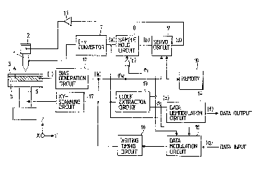
Figure 1 is a block diagram of the apparatus of the
present embodiment. In Figure 1, the reference numeral
1 designates a probe electrode, and the reference
numeral 2 denotes a piezo-actuator for driving the
probe electrode 1 in Z direction. The reference numeral
3 designates a recording layer, the reference numeral
4 denotes a base elec~rode, the reference numeral
5 designates a substrate, and the reference numeral
6 denotes an XY stage. The reference numeral 7 desig-
nates an I-V converter for detecting a tunnel current
flowing between the prohe electrode and the base
electrode through the recording layer 3 and converting
it into a voltage signal. The reference numeral 8
denotes a sample hold circuit for holding the output
20 voltage value (a) of the I-V converter 7 at: the timing
by OR(c) of clocks ~1 and ~w. The reference numeral
9 designates a servo circuit for effecting calculation
from the output voltage (b) of the sample hold circuit
8 and calculating a voltage (d) output to a Z-axis
control actuator. The reference numeral 10 denotes
a memory for storing the control variable of the servo
circuit therein, the reference numeral 11 designates
2 ~ 7 ~
1 a driver for driving the actuator 2, and the reference
numeral 12 denotes a bias generation circuit for
generating reading-out bias and recording pulse voltage
(i~ in the base electrode~ The reference numeral
13 designates a clock extraction circuit for separating
and extracting a reproduction clock signal ~1 and data
recording timing ~2 recorded on the recording layer
from the output of the I-V converter 7. The reference
numeral 14 denotes a data demodulation circuit for
demodulating data recorded on the recording layer.
The reference numeral 15 designates a data modulation
circuit for modulating recording data imparted from
the outside and sending writing pulse data to a writing
timing circuit 16 and the bias generation circuit 12.
The writing timing circuit 16 produces timing ~w~h~
for generating a writing pulse voltage. The reference
numeral l7 denotes a scanning circu:it for driving and
controlling an XY stage so that the probe electrode
may pursue data rows on a recording medium.
Figure 2 is a detailed block diagram of the
servo control circuit 9, and Figure 3 is a detailed
block diagram of the clock extraction circuit 13. In
the servo control circuit of Figure 2, the reference
numeral 91 designates an A/D converter for converting
25 the sample hold output signal (b) into a digital signal,
and the reference numeral 92 denotes a signal processor
for effecting the calculation of servo control. The
- 13 - 2 ~ q)
1 memory 10 for storing the control variable therein
is connected to the signal processor 92. The reference
numeral 93 designates a D/A converter for converting
the calculation output of the signal processor into
an analog voltage, and the reference numeral 94 denotes
a holder for eliminating the output glitch of the D/A
converter and obtaining a smooth analog output (d~.
Also, in the clock extraction circuit of Figure
3, the reference numeral 131 designates a waveform
shaping circuit for shaping the waveform (a) of the
I-V conversion output and passing a clock signal
component therethrough, the reference numeral 132
denotes a phase detection circuit, the reference numeral
133 designates a low-pass filter, and the reference
numeral 134 denotes a voltage control type oscillator
(VCO). The phase detection circuit 132 is a circuit
for phase-detecting the output of the waveform shaping
circuit 131 by a signal obtained by frequency-dividing
the oscillation output of the VCO 134 by a frequency
divider 135. The VCO 134 effects the oscillation of
a frequency proportional~to the output voltage of the
low-pass filter 133, and the output of this VCO is
put out as a reference signal (hereinafter referred
to as the reproduction clock signal) which provides
25 the reference during data reproduction. The reference
numeral 136 designates a phase correcting circuit,
and the reference numeral 137 denotes a phase ~ shifting
circuit.
7 P~
- 14 -
1 Figure 4 shows a timing chart of the signals
of various portions of the apparatus of the present
embodiment shown in Figure 1 during the reproducing
operation. Figure 5 shows a timing chart of the
signals of the various portions during the recording
operation. The present embodiment is characterized
in that on a recording medium, a data bit is written
between adjacent reproduction clock signal bits.
Description will first be made of the operation
of the apparatus of the present embodiment during data
reproduction. The reproducing operation is performed
with a reproduction clock signal as the basic timing.
The reproduction clock signal is extracted from the
signal of recording data. The clock extraction circuit
shown in Figure 3 constitutes a so-called phase locked
loop (PLL) circuit, and effects oscillation phase-
synchronized with a clock signal component included
in a tunnel current signal. A clock ~1 and a clock
~2 differing therefrom by a phase ~ are obtained by
this circuit.
In Figure 4, (a) shows an I-V conversion output
when the XY stage is driven and the probe electrode
scans on a data row written on the recording layer.
(b) shows a signal obtained by sampling the I-V conver-
sion output by the use of the reproduction clock ~1~
and this becomes an input signal to the servo circuit
which effects the Z control of the probe electrode.
- 15 - ~J~
1 As is apparent from Figure 4, the servo control output
(d) of the Z control is effected by the tunnel current
value on the reproduction clock signal bit. Therefore,
the Z control of the probe electrode can be effected
with the reproduction clock signal bit as the reference
without being affected by the information of the data
bit. Also, as regards the demodulation of the data
signal, the I-V conversion output ~a) i~ judged by
a data clock ~2(e) obtained by phase-shifting from
the reproduction clock s~gnal and the logical value
(f) of the reproduction signal is obtained. Like this,
the Z interval control of the probe electrode is effected
by the clock ~1~ and the data bit is reproduced by
the clock ~2 differing in phase from the clock ~1-
The operations of the apparaLtus of the present
embodiment during data recording and during erasing
will now be described with reference to the timing
char~ of Figure 5. In Figure 5, (a) shows the output
of the I-V converter 7 and hatched portions indicate
a tunnel current created by writing and erasing pulse
voltages being applied. --(b) shows the output of the
sample hold circuit 8, and in the case of the recording
operation, it is controlled by a signal (c) which assumes
the logical sum of the reproduction clock ~1 and the
25 writing pulse timing ~w When the signal (c) is a
true value (1)/ the input signa] (a) is intactly output
to (b), and when the signal (c) is a false value (0),
2 ~ 7 ~
- 16 -
1 the input signal (a) when the signal (c) is the true
value immediately before is held and output to tb).
Also, ~w demands the change (h) of a control parameter
to the servo control circuit 9. When the signal ~w
becomes the true value, the servo control circuit 9
temporarily stores the current servo input (b) and
output (d) and a parameter or the like being used for
calculation into the memory 10. Then the parameter
used during writing is loaded from the memory 10 into
the servo control circuit 9. The parameter temporarily
stored into the memory 10 is returned after the
term; n~tion of writing.
The writing pulse voltage is determined by
the comparison between the value of the tunnel current
(signal ~a)) immediately after the rising of ~w and
the logical value to be recorded. That is, the logical
vallle already written on the recording layer immediately
before the writing pulse is generated is detected and
compared with a logical value to be now recorded, and
only when the two logical values differ from each other,
a pulse voltage for inverting the logical values i5
applied, and when the two logical values coincide with
each other~ the application of the pulse voltage is
not effected.
For the servo control of the probe electrode
in Z direction when the writing pulse .is applied, a
control variable suited for the characteristic of the
J ~
1 recording layer is chosen. Where data bits are formed
by variations in the shape of the recording layer,
the probe electrode is displaced away from the recording
layer simultaneously with the application of the pulse.
If at this time, the tunnel current is always monitored
and the amount of energy poured into the recording
layer is controlled, wriking better in reproducibility
can be accomplished. Also, where the formation of
data bits is effected by modulating the electron state
of the recording layer, the optimal value of the spacing
between the tip end of the probe electrode and the
recording layer during the application of the writing
pulse is calculated and applied, and during the applica-
tion of the pulse, the probe electrode is kept so as
lS not to be displaced from this optimal value. If at
this time, the tunnel current is monitored and the
amount of energy poured into the recording layer is
controlled by modulating the applied pulse, writing
much better in reproducibility can be accomplished.
When the pulse is to be applied, the application
of the pulse may be effected with the movement of the
XY stage being temporarily stopped by the utilization
of the writing timing ~w If such operation is performed,
it can be avoided for the recording bit to be distorted
25 in the scanning direction of the recording medium.
The servo control system used in the present
invention permits the application of various techniques
-
- 18 -
1 in accordance with the characteristic of the recording
layer. For example, the PID control widely used
irrespective of an analog or digital system can easily
change the control variable by only three kinds of
5 parameter changes. Further, to effect optimal control,
it is preferable to effect the rule control as known
in Fuzzy Theory by the use of the tunnel current and
the amount of displacement of the probe electrode and
the differentiated and inte~rated values thereof. Also,
to further enhance the stability of recording, it is
preferable to effect control by the use also of the
parameter of the amount of charge or the total amount
of energy poured into the recording layer by the applied
pulse voltage and the tunnel current.
~lso, in the above-described embodiment, signal
modulation is effected at the timing whereat the
recording data is inserted between the reproduction
clock signals, whereas the present invention is not
restricted to such modulation system, but use can be
made of any modulation system which can extract a clock
component from a recorded data ~it.
For the recording layer of the present invention
used for recording and reproduction, use can be made
of various materials if they can detect the information
written on the recording layer by a tunnel current
flowing between the probe electrode and the recording
layer. For example, in a case where unevenness is
-- 19 --
1 formed on the surface of the recording layer to thereby
accomplish recording, mention may be made of an HOPG
(highly-oriented-pyrolithic-graphite) cleavage substrate,
an Si wafer, metal thin film o~ ~acuum-evaporated or
epitaxial-grown Au, Ag, Pt, Mo, Cu or the like, and
glass metals such as Rh25/ Zr75 and Co35Tb65. On the
other hand, in a case where recording is effected by
a change in the electron state of the recording layer,
mention may be made of a thin film layer of amorphous
Si, ~ electron line organic compound or chalcogen
compound.
Also, various shapes and substrate materials
of the recording medium used in the present inven*ion
are conceivable. For example, as the shapes, mention
15 may be maae of a card-like or tape-like substrate,
a disk-like substrate, etc., and as the materials,
mention may be made of a cleavable crystal substrate
such as HOPG or mica, a crystal substrate o~ Si,
sapphire or MgO having its surface polishedl mo].ten
20 quartz, Corning No. 7059 glass, etc. E'urther, as
materials usable also as the substrate materials of
a tape-like medium, mention may be made of polycarbonate,
acryl, PEEK, PET, nylon, etc.
According to the present invention, reproduction
25 of data can be accomplished at a high speed without
the probe electrode colliding with the recording layer.
Further, even if there i.s irregularity in the shape
2 ~ 7 ~'
20 -
l or the electron state of data bits recorded on the
recording layer, reproduction of high S/N ratio can
be accomplished.
Also, during recording, any variation in the
recording conditions by the film thickness dependency
of the recording layer on locations or the irregularity
of the physical property value o~ the recording layer
can be coped with and stable data bits of good
reproducibility can be formed.
Also, even on a recording medium on which
recording has already been effected, data writing can
be effected while erasing is ef~ected. Further,
recording and reproduction which are low in the rate
of error occurrence even if the re-writing of data
is repetitively effected become possible.