Note: Descriptions are shown in the official language in which they were submitted.
' 2066S67 - ~ PCT/DE90/00086 - 1/1 - GR 89 P 1814P
Replacement Page
Circuit arrangement with at least one input and at least
one output for forwarding an input signal that can be
filtered, parallelized and digitized.
The invention relates to a circuit arrangement
with at least one input and at least one output for
forwarding an input signal that can be parallelized and
digitized.
Circuit arrangements of this type are employed
for example for a coupling network component of a network
node in a packet-switching data network.
An N-to-N knockout switching node for a high-
( performance packet-switching system is described in
Patent Specification US-4760570. This is likewise
described by the authors Y.S. Yeh, M.G. Hluchyj and A.S.
Acampora in the IEEE Journal on Selected Areas in Com-
munication, Volume SAC-5, No. 5, 1987, on pages 801-808
in an article entitled 'iThe Knockout Switch: A Simple
Modular Architecture for High-Performance Packet Switch-
ing" as a circuit arrangement which is composed of a
plurality of inputs and a plurality of outputs, and which
is provided for a filterable forwarding of a serial data
packet from one of the inputs to an output that can be
determined from the data packet. Data packets are fil-
tered out by means of a filter connected directly down-
stream of the input. These data packets that can be inputserially at the input aré forwarded serially in a
concentrator. The concentrator is here a matrix-shaped
permutation circuit composed of basic elements, from
which the data packet is forwarded serially bit by bit.
The data packets are forwarded serially from the
concentrator into a shifter. A serial routing and serial
forwarding for a temporary storage in packet memories,
into which the data packets are serially read simulta-
neously from case to case and serially read out again, is
carried out for the serial data packet stream by means of
the shifter. A common buffer composed of shifters and a
specific number of packet memories is provided for each
2~66567
PCT/DE90/00086 - 1/2 - GR 89 P 1814P
Replacement Page
of the outputs. The serial data packet stream from a
comparatively large number of inputs can be concentrated
and stored in a buffer assigned to the output via a
plurality of concentrators with upstream filters by means
Y~
- ' - 2 - 206~567
of an interconnection provided for each of the outputs.
The routing of the data packet stream is carried out
decentrally and locally. The relevant output for for-
warding the data packet is determined from the data
packet in the filters. All the data packets that are not
destined for the output assigned to the filter are
extracted by means of the filter. Except for the storage
in the packet memory, the data packets are otherwise
always forwarded serially. This so-called KO switch is
free of internal blockages since the path of the serial
data packet from the input to the output is not corre-
lated with the path of other serial data packets to other
outputs. Depending on the number of packet memories per
output, external blockages can be prevented. Data packets
that arrive simultaneously at a plurality of inputs and
are destined for the same output can be temporarily
stored in the packet memories of the buffer.
The authors Thomas A., Coudreuse J.-P. and Servel
M. describe in an article entitled "Asynchronous Time-
Division Techniques: An Experimental Packet NetworkIntegrating Videocommunication" at the Symposium ISS '84
Florence, Italy, 7th to 11th May 1984, Session 32 C Paper
2, a switching node which is called "Prélude". Given an
external bit rate of 280 megabits per second on the input
and output lines and with 35 megabits per second inter-
nally, low loss rates and delays can be achieved even
with a high load. Control and storage are carried out
centrally. The 16-byte long packets arriving on the 16
input lines of the node are synchronized and are read
into the central packet buffer byte by byte offset by one
byte in each case. This technique is also termed "para-
gonal", which is derived from parallel-diagonal. The
central control unit performs the translation of the
virtual connection addresses and initiates the entry, at
which the respective packet is located in the central
packet buffer. The entry is made in a queue assigned to
the corresponding output, this queue being processed in
the order of entry. The paragonal structure of th~
preprocessing of the data packets relieves the load on
2066567
'~ PCT/DE90/00086 - 3/1 - GR 89 P 1814P
Replacement Page
the central control unit.
Offenlegungsschrift EU-0263418-A2 discloses a
switching network for switching digital input signals
which arrive on input lines to digital output signals
which are output on output lines, so that the input
signals are synchronized and combined block by block in
time slots, and also that a multiplex signal is obtained
which is combined into multiplex blocks block by block
from the input signals synchronized in time slots, and
also that the multiplex blocks of the multiplex signal
can be exchanged with one another for forming a switched-
through multiplex signal, and also that the multiplex
blocks of the switched-through multiplex signal are
converted and are output block by block as output sig-
nals. A switching control signal, a so-called connection
control signal, is required, by means of which it is
defined which of the input lines is to be switched
through to which of the output lines in time slots, so
that the exchange of the multiplex blocks is controlled
by this switching control signal.
The object of the invention is to disclose a
further circuit arrangement for forwarding a signal that
can be parallelized and digitized, preferably a serial
data packet with a particularly high bit rate, from an
input to an output that can be determined from the
signal.
This object is achieved in a circuit arrangement
with at least one input and at least one output for
forwarding an input signal that can be filtered, paral-
lelized and digitized, having the following features:
a) the input signal (8) that can be input at an input
(80) of the circuit arrangement (1000, 2000) can be
fed to an input signal form converter (60) for input
conversion into an at least partially parallelized bit
group packet signal (1) composed of at least one
parallel bit group,
b) connected upstream of an output (90) of the circuit
arrangement (1000, 2000) is an output signal form
2066a67
- l~ PCT/DEso/00086 - 3/2 - GR 89 P 1814P
Replacement Page
converter (30) for output conversion of the bit group
packet signal (3) into an output signal (9) that can
be output at the output (90),
c) a forwarding means (20) is provided for the parallel
forwarding of the bit groups from the input signal
form converter (60) to the output signal form con-
verter (30),
d) an intermediate memory (40) is provided for temporar-
ily storing at least one of the bit groups of the bit
group packet signal,
e) an output filter (50) is provided for filterable
forwardinq of the bit group packet signal, which
- filter has to determine the relevant output
for the forwarding from the bit group packet signal.
The invention is based on the perception that it
is possible to reduce the internal operating speed by
means of a parallelization provided directly at the
input, a temporary storage and a conversion provided
directly at the output, and in particular it is possible
to forward under decentralized control a particularly
high external serial bit rate converted internally to
parallel.
The input signal may be provided here in an
optical or electronic input signal form that can be
digitized and parallelized.
In the input signal form converter, the signal
can be converted into a bit group packet signal which is
composed of one or more bit groups.
In the output signal form converter, the output
signal can be formed from the bit group(s) of the bit
group packet signal.
A circuit arrangement with only one input and
only one output can be used for example for a delaying,
code conversion, conversion of the signal or extraction,
it being possible to determine from the signal whether
the signal is forwarded to the output or extracted.
The parallel forwarding of the bit group packet
signal internally is preferably carried out in bit
7 ~ 5 ~ 7 -
,- "~ PCT/DE90/00086 - 3/3 - GR 89 P 1814P-
Replacement Page
groups.
At least one bit group of the bit group packet
signal can be temporarily stored in an intermediate
memory.
~he relevant output for the forwarding can be
2 0 6 6 ~ 6 7
- 4
determined from the bit group or the bit groups of the
bit group packet signal. The forwarding of a bit group
packet signal can be blocked or released.
In the case of a particularly wide parallel-
ization of the input signal in the input signal formconverter, the internal operating speed can be reduced
very considerably. As a result of a decentralized tempor-
ary storage, advantages are conferred with regard to the
operating speed of the forwarding means. While the
central control may often be overloaded in the case of a
centrally controlled network node, this is advantageously
avoided in the decentralized concept according to the
invention.
Depending on the application, the bit groups of
the bit group packet signals are temporarily stored for
example according to a pure input memory principle, or
for example according to a pure output memory principle,
or for example according to a combination of both prin-
ciples, or for example according to none of these prin-
ciples. Moreover, in certain applications it is sensibleif the temporary storage is provided, for example, in a
bit group register which has additional functions, and is
employed, for example, as shift register in the input
signal form converter or in the output signal form
converter for example. For special applications it is
expedient for the forwarding means to forward bit groups
step-by-step from bit group register to bit group regis-
ter. For known bit-serial arrangements, of a banyan
structure for example, or of a hyperconcentrator for
example, or of merge boxes for example, or other known
bit-serial structures, the operating speed can be reduced
decisively as a result of the parallelization according
to the invention, so that instead of one intermediate
memory for one bit in each case in the known arrange-
ments, according to the invention a bit group register isprovided for a parallel temporary storage of a wide bit
group. In this case, as a result of the parallelization,
the internal operating speed can be reduced, in particu-
lar for a parallel forwarding or temporary storage of the
. ~ 5 7 ~
bit groups. Of the wide variety of advantageous applica-
tions of the invention, particularly preferred embodi-
ments are described in the text that follows.
One preferred embodiment of the invention is
characterized in that an input signal form of the input
signal and an output signal form of the output signal are
identical and are a clock-controlled serial, digital and
electronic data packet. As a result, a plurality of
circuit arrangements can advantageously be interconnected
in a simple manner, for example in a network node of a
packet-switching data network. The data packet is com-
posed, for example, of organizational part and data part.
The organizational part frequently contains the address
signal, by means of which it is possible to determine the
relevant output of the circuit arrangement for the
forwarding.
A further preferred embodiment of the invention
is characterized by an output shift register of the
output signal form converter, into which the bit group
packet signal can be input in bit groups in parallel, and
from which the output signal can be serially output. The
bit group packet signal may be composed here of one or
more bit groups. The width of the output shift register
may be equal to the number of bits in the bit group. In
each case one bit group of the bit group packet signal
can be input in parallel into the output shift register
with each output clock pulse, which may be equal, for
example, to the bit group clock pulse divided by the
number of inputs. In accordance with the bit clock pulse
of the data packet, the data packet can be output seri-
ally from the output shift register. The output signal
form conversion can be advantageously accomplished by a
simple output shift register.
A further preferred embodiment of the invention
is characterized by an input shift register of the input
signal form converter, into which the input signal can be
input serially, and from which the bit group packet
signal can be output in bit groups in parallel. The input
signal form conversion can be accomplished in a simple
~ 6 - 2066~67
manner by a simple input shift register.
A further preferred embodiment of the invention
is characterized in that the forwarding means has a bit
group bus. In an advantageous manner, the bit group
packet signal can be forwarded by means of the bit group
bus from one unit of the circuit arrangement simulta-
neously to one or more units of the circuit arrangement.
A width of the bit group bus can preferably be provided
in the width of the bit group.
A further preferred embodiment of the invention
is characterized by a bit group memory of the forwarding
means for storing the bit groups in bit group memory
registers. To avoid external blockages, data packet
signals can be stored in groups, for example, in the bit
group memory registers of the bit group memory, so that
data packets arriving simultaneously at a plurality of
inputs of the circuit arrangement can be stored by means
of the bit group memory and can be forwarded in succes-
sive data packets and output to an output. The width of
the bit group memory register is frequently also referred
to as the word width of a memory word of the bit group
memory. The bit group memory may be provided here accord-
ing to a first-in-first-out principle. Bit group memories
of this type can be realized in a known simple manner.
For example, a FIF0 memory with address registers can be
employed likewise for the input and the output of bit
groups. A FIFO memory with shift registers can also be
used. Further embodiments of the bit group memory accord-
ing to another principle may also be used. For example,
a buffering can be provided by means of direct addressing
or addressing by means of address registers, in connec-
tion with a serializing of the stored bit group packet
signals. The urgent forwarding of a bit group packet
signal with priority can be marked here in the bit group
packet signal or be derived from the input at which the
data packet was input. For example, a data packet input
at the first of the inputs is forwarded urgently with
priority in comparison with the data packets input at the
other inputs.
2066367
A further preferred embodiment of the invention
is characterized in that a number of packets of the bit
group packet signals equal to the number of inputs can be
stored in the bit group memory. Depending on the number
of packets that can be stored in the bit group memory, an
average packet loss probability emerges from the traffic
profile of the incoming data packets and the switching
load. The greater the number of packets for the bit group
packet signals that can be stored in the bit group
lo memory, the lower the average packet loss probability is
given a comparatively equal number of incoming data
packets. Given an average switching load and approximate-
ly evenly spread traffic profile, the average packet loss
probability is sufficiently low with this preferred
embodiment of the circuit arrangement.
A further preferred embodiment of the lnvention
is characterized by at least one index register of the
bit group memory for addressing the bit group memory
registers. In particular in the case of a cyclical use of
the bit group memory registers, the index register may be
incremented here and employed as counter register.
A further preferred embodiment of the invention
is characterized in that the bit group memory is an
output memory assigned to the respective output for
2S storing bit groups of bit group packet signals to be
forwarded to the assigned output. The bit group memory
may be here the memory element of an output queue. In
comparison with input queues, output queues have in a
known mann~r the advantage that internal blockages are
avoided and a higher switching load can be achieved.
A further preferred embodiment of the invention
is characterized in that a number of bits in the bit
group is provided which is at least equal to the number
of inputs multiplied by a bit clock pulse of the data
packet divided by a bit group clock pulse conditioned by
a clock pulse unit which is equal to an output memory
clock pulse and likewise to a bit group bus clock pulse.
The width of parallelization may be defined by the number
of bits in the bit group, depending on the output memory
. ~ - 8 - 2066~67
clock pulse and on the number of inputs. The bit group
bus clock pulse may be equal to the output memory clock
pulse. As a result, bit groups from all inputs can be
stored in the output memory. The bit groups can be
forwarded by means of the bit group bus from the input
signal form converter to an output memory or simulta-
neously to all output memories. In this case, a temporary
storage of one or more of the bit groups can be provided
in a bit group register or in an input memory, which may
be provided directly in the input signal form converter
or be connected directly downstream thereof. The bit
groups can be fetched in sequence in cyclical order from
all inputs from the bit group registers or the input
memories by means of the bit group bus and forwarded to
the output memory or simultaneously to all output mem-
ories connected to the bit group bus. In a preferred
embodiment, the output filter can be connected directly
upstream of the output memory or be provided directly in
the memory input part of the output memory. An advantage-
ously low main memory clock pulse can be achieved with aparticularly wide parallelization with a large number of
bits in the bit group.
A further preferred embodiment of the invention
is characterized in that the input signal can be con-
verted in the input signal form converter into a plural-
ity of successive bit groups of the bit group packet
signal, it being possible to determine the relevant
output for the forwarding from the first bit group. The
output filter can ascertain from the first bit group the
relevant output for the forwarding of all bit groups of
the bit group packet signal of a converted data packet.
In one of the preferred embodiments mentioned, the output
filter may be incorporated in the input signal form
converter. In this case, it is possible to ascertain from
the first bit group of the bit group packet signal of a
converted data packet whether this first and the further
following bit groups of the bit group packet signal are
to be released or to be blocked for the forwarding. If
forwarding is to be blocked, the forwarding of the first
2~66567
g
converted bit group is blocked or disabled, likewise for
all following bit groups until the arrival of the next
bit group packet signal of a converted data packet. In
another embodiment mentioned, the output filter can be
connected directly upstream of the output memory or be
integrated therein. In this case, for example, by means
of the bit group bus clock pulse it is possible to
ascertain from which input signal form converter the bit
group received originates, so that the latter can be
assigned to a bit group packet signal. The division of
the bit group packet signal into a plurality of succes-
sive bit groups can advantageously permit a smaller
number of bits in the bit group, which makes a smaller
bit group bus width possible, which may be advantageous
in particular if the output memory clock pulse is only
low or is smaller by a few magnitudes in comparison with
the bit clock pulse of the data packet.
A further preferred embodiment of the invention
is characterized by a serializing means of the output
memory, by means of which the bit groups input into the
output memory can be output in series in successive bit
group packet signals. By means of the bit group bus clock
pulse it is possible to ascertain, for example, from
which input signal form converter the bit group received
via the bit group bus originates. The bit group can thus
be assigned to the bit group packet signal, so that from
this the serializing means of the output memory initiates
or controls the storage of the bit group in the respect-
ive bit group memory register provided and reserved for
storing the bit group. The addressing of the respective
bit group memory register can be carried out here, for
example, with the assistance of the index register, or
one of the index registers, of the bit group memory. In
accordance with the output clock pulse, the memory output
of the bit group can be carried out by the serializing
means of the output memory with the assistance of the
index register, or one of the index registers, for
addressing the bit group memory register. All bit groups
of a bit group packet signal are output here successively
20~6~67
-- 10 --
in accordance with their order. Following this, the
stored bit groups of the next bit group packet signal are
output. With the serializing means it is possible to
initiate that, of a plurality of stored bit group packet
signals, the one which was stored first is output first.
The combination of the bit groups to form bit group
packet signals and the order of the bit group packet
signals can advantageously be initiated or controlled by
the serializing means. An additional queue organization
is consequently unnecessary, because as a result of the
serializing means of the output memory the storage of the
bit groups in the output memory can be carried out
cyclically in accordance with the addressing of the bit
group memory registers, ordered according to bit group
packet signals, and within the bit group packet signals
ordered according to the order of the bit groups of the
bit group packet signals. This embodiment can be advan-
tageously applied in particular for the forwarding of
particularly long data packets or digitizable signals of
a particularly large number of bits.
A further preferred embodiment of the invention
is characterized by a bit group packet signal composed of
a single bit group. In this case, an entire bit group
packet signal can be forwarded in the circuit arrangement
with each bit group. Given employment of the output
memory, the additional serializing of the bit groups for
the combination of bit group packet signals in the output
memory can be dispensed with here. This embodiment can be
advantageously applied in particular given a comparative-
ly low number of bits in the bit group packet signal.Moreover, in the case of an especially wide bit group
bus, the bit group memory clock pulse is particularly low
in an advantageous manner in comparison with the bit
clock pulse of the data packet. Of a plurality of input
and stored bit groups, in each case the bit group input
first can be output first by an output means of the
output memory. In accordance with the addressing of the
bit group memory registers, these can be written cycli-
cally for example. The addressing of the bit group memory
2066~67
. "_
11
registers can be carried out here for example with the
assistance of the index register or index registers of
the bit group memory. The output means can thus be
realized in a simple manner.
A further preferred embodiment of the invention
is characterized by an input stage assigned to the input
which is composed of an input memory as intermediate
memory and of the input shift register. The width of the
input shift register may be equal to the number of bits
10 in the bit group. In each case one bit group can be
output in parallel here to the input memory from the
serial data packet with each input clock pulse. The input
memory may be provided here according to a first-in-
first-out principle, and be able to store, for example,
15 the bit groups of at most two bit group packet signals in
its bit group registers. Given employment of the bit
group bus, the latter can sequentially fetch in each case
all bit groups of an entire bit group packet signal from
one of the input memories, and can afterwards sequential-
20 ly fetch in each case all the bit groups of a further bit
group packet signal from a further one of the input
memories. In this manner, as a result of the temporary
storage and as a result of the collecting of the bit
groups in the input memories, entire bit group packet
25 signals can be put together in these. If such input
memories are employed, given employment of output mem-
ories for these, the serializing of the bit groups to
form bit group packet signals can be dispensed with. The
input memory can also be designed as a tandem buffer for
30 input and output of a bit group packet signal in each
case. By virtue of the input stage, a component of the
circuit arrangement, which can be advantageously employed
in particular for extensions, can be formed in a simple
manner.
A further preferred embodiment of the invention
is characterized by an output stage composed of the
output shift register, the output memory and the output
filter. Bit group packet signals can be forwarded to the
output stage of the circuit arrangement, it being
2066567
- 12 -
possible to filter out via the output filter those bit
group packet signals whose forwarding is to be blocked
off in the output stage of the circuit arrangement. By
virtue of the output stage, a component of the circuit
arrangement, which can be advantageously employed in
particular forextensions,canbe formedin a simple manner.
In each case one input stage can be provided for
each input and in each case one output stage can be
provided for each output. Each data packet arriving at
the input can be converted in the input shift register,
assigned to the respective input, of the input stage to
form the bit groups of the bit group packet signal
temporarily stored in the input memory. The bit groups
temporarily stored in the bit group registers of the
input memory can be forwarded by means of the bit group
bus of the circuit arrangement and reach the output
memories of the output stage via the output filters. An
output filter can be connected directly upstream of each
output memory or can be integrated therein. The for-
warding can be blocked off directly before the outputmemory or in the output memory. In any case, only those
bit groups whose forwarding to the output assigned to the
output memory is intended are stored in the output
memory. In accordance with the output clock pulse, the
bit groups can be forwarded from the output memory to the
output signal form converter. The bit groups can be
fetched by the bit group bus in accordance with the bit
group bus clock pulse from the input memory of an input
stage and can be simultaneously forwarded to each output
memory via the output filters. In this case, all bit
groups of a bit group packet signal can be forwarded
directly successively from the input memory by the bit
group bus to the output memories.
A further preferred embodiment of the invention
is characterized by an output module assigned to the
output which is connected on the one hand to the assigned
output and on the other hand to each input, and which has
the output memory, the bit group bus, the output signal
form converter and in each case one input part for each
2066a67
~_ - 13 -
input. An internal blocking of the circuit arrangement
can consequently be prevented. Moreover, by virtue of the
output module, a component of the circuit arrangement,
which can be advantageously employed in particular for
extensions, can be formed in a simple manner.
A further preferred embodiment of the invention
is characterized in that the input part has the input
shift register, the output filter and an input memory as
intermediate memory. The output filter may be connected
here directly upstream of the input shift register,
integrated therein or be connected directly downstream
thereof. In each case, only those bit groups whose
forwarding to the output assigned to the output module
has been checked and released by the output filter are
temporarily stored in the input memories. The bit groups
can be forwarded from the input memory to the output
memory of the output module by means of the bit group bus
of the output module. The bit groups of in each case one
bit group packet signal are forwarded to the output
memory by the bit group bus in accordance with the bit
group bus clock pulse from the input memories, assigned
to each input, of one of the input parts. In each case
one bit group can be forwarded from the output memory to
the output signal form converter in accordance with the
output clock pulse. In this type of circuit arrangement
with separate output modules and an output filter direct-
ly in the input part, only those bit groups whose for-
warding to the output assigned to the output module is
inten~e~ are forwarded from the bit group bus of the
respective output module.
A further preferred embodiment of the invention
is characterized by an integrated construction on a
single semiconductor wafer. AS a consequence, in particu-
lar an especially wide bit group bus can be realized.
Given an especially wide bit group bus, the bit group
memory clock pulse can be particularly low in comparison
with the bit clock pulse of the data packet. The basic
material of the semiconductor wafer may be gallium
arsenide for example, or one of the other known
2066S67
14 -
semiconductor materials. Particularly in the case of
gallium arsenide, the known advantages of gallium
arsenide semiconductor technology with respect to the
fast switching times can be conferred thereby.
A further preferred embodiment of the invention
is characterized by a basic material of the semiconductor
wafer made of silicon. The known advantages of cost-
effective silicon semiconductor technology with respect
to the fast switching signals and with respect to the
heat conductance can be conferred thereby.
A further preferred embodiment of the invention
is characterized in that CMOS circuit parts are provided
on the semiconductor wafer. As a consequence, the known
advantages in particular with respect to a low heat
dissipation and in particular with respect to a favorable
stable behavior can be conferred. It is also possible to
provide further electronic circuit parts in addition to
the CMOS circuit parts.
A further preferred embodiment of the invention
is characterized in that BICMOS circuit parts are pro-
vided on the semiconductor wafer. As a consequence, the
known advantages of a combination of bipolar technology
with CMOS technology can be conferred. In particular, the
known advantages of bipolar technology with respect to
speed can be utilized thereby. For example, the input
signal form converter and also the output signal form
converter can be constructed in bipolar technology. For
example, circuit elements for temporary storage, or in
particular for storing the bit groups can be constructed
in CMOS technology.
A further preferred embodiment of the circuit
arrangement according to the invention is characterized
in that its circuit parts are arranged next to one
another on the semiconductor wafer in rectangular areas
with an identical register area width determined by the
number of bits. Owing to the employment of rectangular
register-area-wide areas for arranging circuit parts of
the circuit arrangement, an optimum utilization of the
surface of the semiconductor wafer can be achieved. The
2066S67
- 15 -
registers of the circuit elements, in particular the
input shift register, the output shift register, the bit
group register and the memory inputs as well as the
memory outputs of the input memory and of the output
memory, may be arranged here along the register area
width of the rectangular areas bit by bit in a row.
A further preferred embodiment of the invention
is characterized in that areas to be connected to the
same bit group bus are arranged register area width to
register area width next to one another in each case. In
particular as a consequence of the fact that all the
areas associated with one bit group bus can be arranged
register area width to register area width next to one
another, the line connections of the bit group bus can be
laid in an at least approximately straight line in an
advantageously simple manner. By virtue of these optimum
short line connections, particular advantages for the
transit time during the forwarding of the bit groups can
be conferred.
A further preferred embodiment of the invention
is characterized by the following arrangement on the
semiconductor wafer:
a) the output module is arranged in a register-area-wide
rectangular module area,
b) the module areas identically constructed for each
output in each case are arranged next to one another,
c) input shift registers, output filters and input
memories assigned in each case to each input are
arranged in the output module in a register-area-wide
rectangular input area in each case,
d) the output memory and the output shift register are
arranged in the output module in a register-area-wide
rectangular output areà.
This preferred embodiment can be realized in this
manner with an optimum utilization of the surface of the
semiconductor wafer.
A further preferred embodiment of the invention
is characterized by the following arrangement on the
semiconductor wafer:
20~6~67
".
- 16 -
a) the input stages provided for each input are arranged
next to one another in register-area-wide rectangular
input stage areas,
b) the output stages are arranged next to one another in
5register-area-wide rectangular output stage areas,
c) the input stage areas and the output stage areas are
arranged next to one another,
d) within each input stage area, the input shift register
and the input memory are arranged next to one another,
10e) within each output stage area, the output filter, the
output memory and the output shift register are
arranged next to one another.
This preferred embodiment of the invention can be
realized in this manner with an optimum utilization of
15the surface of the semiconductor wafer.
The invention will be explained in greater detail
with reference to the figures, in which exemplary embodi-
ments are illustrated.
Figure 1 shows a network structure of a data
20network for switching data packets.
Figure 2 shows a network node of the data net-
work.
Figure 3 shows a block circuit diagram of a first
exemplary embodiment of the invention.
25Figure 4 shows a floor plan of the first exemp-
lary embodiment of the invention.
Figure 5 shows a block circuit diagram of a
second exemplary embodiment of the invention.
Figure 6 shows the clock pulse supply structure
30for the second exemplary embodiment of the invention.
Figure 7 shows the clock pulse unit for the
second exemplary embodiment of the invention.
Figure 8 shows clock-controlled switching struc-
tures for the second exemplary embodiment of the inven-
35 tion.
Figure 9 shows an output filter for the second
exemplary embodiment of the invention.
Figure 10 shows a timing diagram for-the second
exemplary embodiment of the invention.
2066~6 1
- ~ - 17 -
Figure 11 shows a floor plan of the second
exemplary embodiment of the invention.
As Figure 1 shows for the following exemplary
embodiments, a network structure of a clock-synchronized
data network for switching data packets is composed, for
example, of three network nodes 5000 and a number of
subscriber terminals 5100. Data packets are generated as
data signals 7 by the subscriber terminals S100 and are
sent to the network nodes S000 for switching. Each data
packet contains an address signal which is evaluated by
the network nodes 5000 and which specifies the respective
subscriber terminal 5100 to which the data packet is to
be sent as data signal 7 by the network node 5000. In
g this case, the data packet can be sent as data signal 7
from one network node 5000 to another network node 5000.
As Figure 2 shows, the network node 5000.1
contains a switching center 5900. The data signals 7
received by the network node 5000.1 are fed as input
signals 8 to the inputs of the switching center 5900. The
output signals 9 are derived from the outputs of the
switching center 5900 as the data signals 7 to be sent by
the network node 5000.1. A clock signal 289 is generated
by a clock generator 5389 and is fed to the switching
center 5900 at the clock input 389.
As Figure 3 shows, the first exemplary embodiment
of the invention is composed of a switching center 5900
I in the form of a circuit arrangement 1000 which has a
plurality of inputs 80 and also a plurality of outputs
90, as well as a plurality of output modules 400. The
output modules 400 are of identical construction in this
arrangement. Each output module 400 has a plurality of
module inputs 480 and one module output 490. The first
module input 480.1 is connected in each case to the first
input 80.1 of the circuit arrangement 1000, the second
module input 480.2 is connected to the second input 80.2,
and further module inputs 480 are connected in each case
to further inputs 80 of the circuit arrangement 1000. The
first module input 480.1.2 of the second output module is
connected to the first input 80.1 of the circuit
2066567
- 18 -
arrangement 1000, the second module input 480.2.2 of the
second output module 400.2 is connected to the second
input 80.2 of the circuit arrangement 1000. Of the
further output modules 400, the first module inputs 480.1
are likewise connected in each case to the first input
80.1 of the circuit arrangement 1000, and further module
inputs 480 of the output modules 400 are connected to
further inputs 80 of the circuit arrangement 1000. The
output 490.1 of the first output module 400.1 is con-
nected to the first output 90.1 of the circuit arrange-
ment 1000, the output 490.2 of the second output module
400.2 is connected to the second output 90.2 of the
circuit arrangement 1000, and the outputs 490 of the
further output modules 400 are connected to the further
outputs 90 of the circuit arrangement 1000.
Each output module 400 has for each input 80 in
each case its own input part 470, which is connected via
the associated module input 480 in each case to the
associated input 80.
Serial data packets can be input as input signals
8 at the inputs 80 of the circuit arrangement 1000. In
this exemplary embodiment, these signals have a length of
256 bits, the direction information being contained at
the beginning of the data packet. It is possible to
ascertain from the direction information of the data
packet whether the data packet is to be extracted or
forwarded to one of the outputs 90 of the circuit ar-
rangement 1000. A data packet, input for example at the
input 80.1, is serially input in each case in one input
part 470.1 of one output module 400 in each case, where
it is stored serially by an input shift register 60.1 in
each case and converted into parallel to form successi~e
bit groups of a bit group packet signal 1. In this
exemplary embodiment, the 256-bit long data packet of the
input signal 8 provided is converted into a bit group
packet signal 1 composed of four bit groups of 64 bits
each, the direction information being contained in the
first bit group, from which it is pO8 S ible to determine
the relevant output for the forwarding. Beginning with a
CA 02066~67 1998-11-0~
-- 19 --
packet clock pulse of the data packet, the data packet of the
input slgnal 8 ls lnput serlally lnto the lnput shlft
reglsters 60.1 ln accordance wlth a blt clock pulse of the
data packet, where lt ls forwarded ln parallel ln accordance
wlth an lnput clock pulse that ls four tlmes as hlgh as the
packet clock pulse. Wlth a wldth of 64 blts, the blt group
packet slgnal 1 is forwarded blt group by blt group ln
accordance wlth an lnput clock pulse lnto the lnput parts
470.1 to the output fllters 50.1 of the lnput parts 470.1,
where the dlrectlon lnformatlon ls checked, and all the blt
groups of the blt group packet slgnal 1 are elther extracted
or successlvely forwarded ln accordance wlth the lnput clock
pulse to an lnput memory 40.1 of the lnput parts 470.1 as the
blt group packet slgnal 5. In accordance wlth the lnput clock
pulse, whlch ls equal to the lnput memory clock pulse, ln each
case one blt group of the blt group packet slgnal 5 can be
temporarlly stored there. The dlrectlon lnformatlon speclfles
that the data packet lnput ls to be forwarded to exactly one
of the outputs 90 or to none of the outputs 90. From each of
the output fllters 50 of the output modules 400, the blt
groups of the blt group packet slgnal 1 are forwarded as bit
group packet slgnal 5 ln each case only lf the output 90
asslgned to the output module 400 ls ascertalned from the
dlrectlon lnformatlon. Accordlngly, an lnput slgnal 8 lnput
at an lnput 80 ls forwarded by exactly one or none of the
output fllters 50. Inner blockages are consequently
prevented. In the same manner, a data packet lnput at an
20365-3164
CA 02066~67 1998-11-0
- l9a -
lnput 80.2 ls converted in the input parts 470.2 to form blt
groups of a blt group packet slgnal, ln the lnput shlft
reglsters 60.2, checked by the output fllters 50.2 wlth
respect to the dlrectlon lnformatlon, and temporarlly stored
ln exactly one or none of the lnput memorles 40.2 blt group by
blt group ln accordance wlth the lnput clock pulse.
There ls provlded ln each output module 400 lts own
blt group bus 20, by means of whlch the blt groups of the blt
group packet slgnal 2 temporarlly stored ln the
20365-3164
~ - 20 - 2066.~67
input memories 40 are forwarded in accordance with a bit
group bus clock pulse which is equal to the number of
inputs 80 multiplied by the input clock pulse. As a
result, all temporarily stored bit group packet signals
can be forwarded from all input memories 40. Owing to
temporary storage of the bit groups of the bit group
packet signals, each input memory has here 8 bit group
registers in each case, so that in each case the bit
groups for a maximum of two bit group packet signals can
be temporarily stored therein. In this arrangement, the
temporary storage of the bit groups is carried out
according to a first-in-first-out principle. Memories of
this type are generally known and can be employed as
- input memories. In this exemplary embodiment, the bit
group bus 20 has a width of 64 bits. A bit group packet
signal with all bit groups is fetched in each case from
one of the input memories 40 in cyclical sequence and is
forwarded, provided that such a bit group packet signal
has been temporarily stored therein.
Provided in each output module 400 is its own
output memory 10, in which the bit groups of the bit
group packet signals 2 to be forwarded are stored in bit
group registers. In this exemplary embodiment, the bit
group memory registers have a width of 64 bits. This
2~ corresponds to the width of parallelization and is equal
to the width of the bit group and equal to the width of
the bit group bus. The memory clock pulse is equal to the
bit group bus clock pulse. In this exemplary embodiment,
the number of bit group memory registers is equal to four
times the number of inputs 80, that is to say, given four
inputs 80 for example, sixteen bit group memory registers
are provided. Four bit groups are stored for each bit
group packet signal 2, so that in total it is possible to
store a number of bit group packet signals equal to the
number of inputs 80. The temporary storage of the bit
groups is carried out here according to a first-in-first-
out principle. Memories of this type are generally known
and can be employed as output memories.
If, for example, two data packets are input
- 2066S67
- 21 -
simultaneously at the input 80.1 and at the input 80.2,
both of which are intended for forwarding to the output
90.1, then the first bit group of the respective bit
group packet signal for both in each case is temporarily
stored in the input memories 40.1.1 and 40.2.1 at the
input clock pulse. At the next following bit group bus
clock pulse, the bit group temporarily stored in the
input memory 40.1.1 does not yet form a complete bit
group packet signal, so that this is ascertained by the
bit group bus 20.1 and a forwarding is not yet carried
out to begin with until all bit groups of a bit group
packet signal are temporarily stored in the input memory.
At the next input clock pulse, in each case the second
( bit groups of the bit group packet signals are temporar-
ily stored in the input memories 40.1.1 and 40.2.1. At
the next input clock pulse, in each case the third bit
groups of the bit group packet signals are temporarily
stored in the input memories 40.1.1 and 40.2.1. At the
next input clock pulse, in each case the fourth bit
groups of the bit group packet signals are temporarily
stored in the input memories 40.1.1 and 40.2.1. After
this, with the next four bit group bus clock pulses in
each case, the four bit groups of the bit group packet
signal are read out of the input memory 40.1.1 by means
of the bit group bus 20.1 and are read in each case into
the output memories lO.1 and stored. After this, with the
next four bit group bus clock pulses in each case, the
four bit groups of the bit group packet signal are read
out of the input memory 40.2.1 by means of the bit group
bus 20.1 and are read in each case into the output
memories 10.1 and stored. Following this, a bit group is
output from the output memory 10.1 at the output clock
pulse in each case, and in this exemplary embodiment is
read in parallel with a width of 64 bits into the output
shift register 30.1. From the output shift register 30.1,
the bit group is read out serially with the bit clock
pulse and is output as output signal 9 at the output
90.1. The bit groups read into the output memories are
read out into the output shift registers according to a
2 0 6 6 ~ 6 7
- 22 -
first-in-first-out principle.
In each output module 400, in each case the bit
groups are output by the output memory 10 to an output
signal form converter 30 of each output module 400. In
one output shift register 30 of each output signal form
converter 30 in each case, the bit groups of the bit
group packet signal 3 are input in parallel in each case
at the output clock pulse, and the data packets of the
output signal 9 are formed serially in accordance with
the bit clock pulse and are output via the module outputs
to the respective output 90.
Provided in each olltput module 400 is a clock
pulse unit 200 which synchronizes 2nd conditions respect-
( ive output module 400 the
packet clock pulse, the bit clock pulse, the input clock
pulse, the output clock pulse, the bit group bus clock
pulse or input memory clock pulse and the output memory
clock pulse.
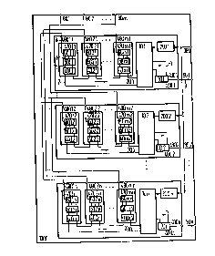
As Figure 4 shows, the circuit arrangement 1000
according to Figure 3 is constructed in this exemplary
embodiment on a single semiconductor wafer 3000. A floor
plan that is described below i8 employed here. The output
modules 400 are arranged next to one another in register-
area-wide rectangular module areas 3400. Each module area
3400 contains one output area 3430 in each case, as well
as one input area 3470 in each case for each input 80.
~F
The register-area-wide rectangular output area 3430
contains in each case the output shift register 30 in a
register area 3030 and the output memory 10 in a memory
area 3010. Each input area 3470 contains in each case in
an input shift register area 3460 the input shift regis-
ter 60, the output filter 50 in an output filter area
3450, and the bit group registers of the input memory 40
in a bit group register area 3440. The register area
width 33 is characterized in that in this exemplary
embodiment, the number of bits in the bit group is 64,
and in that the flip-flop storing one bit in each case of
the registers storing the bit groups, for example input
shift registers, bit group registers of the input
2066567
- 23 -
memories, bit group memory registers of the output
memories, output shift registers, are arranged in at
least approximately a row. These registers are arranged
in each case in a rectangular area, the one rectangle
side of which corresponds to the register area width 33.
These registers are arranged next to one another
register area width 33 to register area width 33. This
results in particularly short line connections for the
forwarding of a bit from one register into the correspon-
ding bit of the other register, and also particularlyshort signal transit times. This applies in particular to
the bit group bus, which in this exemplary embodiment is
composed of 64 line connections 22 in each case, on which
the bits of the bit groups are forwarded in parallel. The
connection of the inputs 80 to the module inputs is
carried out via input connections 88. This floor plan
results in a particularly optimum surface utilization on
the semiconductor wafer.
As Figure 5 shows, the second exemplary embodi-
ment of the invention is composed of a switching center5900 in the form of a circuit arrangement 2000, which has
a plurality of inputs 80 and also a plurality of outputs
90. Each of the inputs 80 is connected to exactly one
input stage 70, which has an input shift register 60 and
an input memory composed of exactly one bit group regis-
ter 40. Provided for each of the outputs 90 is an output
stage 100 which has an output filter 50, an output memory
10 and also an output shift register 30 as output signal
form converter. The bit group forwarding means has a bit
group bus 20 which connects the input stages 70 to the
output stages 100.
Serial data packets can be input as input signals
8 at the inputs 80 of the circuit arrangement 2000, which
signals have a length of 128 bits in this exemplary
embodiment, the direction information being cont~ine~ in
the data packet. It is possible to ascertain from the
direction information of the data packet whether the data
packet is to be extracted or forwarded to one of the
outputs 90 of the circuit arrangement 2000. A data packet
2066~7
- 24 -
8.1, input for example at the input 80.1, is serially
input into the input stage 70.1, where it is stored
serially by the input shift register 60.1 and converted
into parallel to form exactly one bit group of the bit
group packet signal 1.1, which in this exemplary embodi-
ment is exactly one bit group of 128 bits. Beginning with
a packet clock pulse of the data packet, the data packet
is input serially into the input shift register 60.1 in
accordance with a bit clock pulse of the data packet,
where it is forwarded in parallel into the bit group
register 40.1, which is employed as input memory in this
exemplary embodiment, in accordance with an input clock
pulse that is equal to the packet clock pulse in this
exemplary embodiment. In accordance with a bit group bus
clock pulse, which in this exemplary embodiment is equal
to the number of inputs 80 multiplied by the packet clock
pulse, the bit group packet signals 1 temporarily stored
in the bit group registers 40 are forwarded by the bit
group bus 20, so that all temporarily stored bit group
packet signals can be forwarded from all bit group
registers 40 between two input clock pulses. In this
exemplary embodiment, the bit group bus 20 and all
registers provided for temporarily storing or storing the
bit group of the bit group packet signal, that is to say
the input shift registers 60, the bit group registers 40,
the output shift registers 30 and also the bit group
memory registers of the output memories 10, have a width
of 128 bits. With each bit group bus clock pulse, in each
case one of the bit group registers of the input memories
40 is interrogated in cyclical sequence. From the bit
group bus 20, a bit group 2 is forwarded with the same
bit group bus clock pulse from one of the bit group
registers 40 via the output filters 50 connected directly
upstream of the output memories 10 to all output memories
10 simultaneously in each case. Connected upstream of
each of the outputs 90 is in each case an output signal
form converter 30 and also an output memory 10 and an
output filter 50, which form in each case the output
stage 100 assigned to this output 90. The output filter
2 0 6 6 ~ 6 7
25 -
50 checks on the basis of the direction information of
the bit group 2 forwarded by the bit group bus 20 whether
the bit group 2 is to be forwarded to the assigned output
90 or extracted. As a result, only those bit groups whose
forwarding to the assigned output 90 is intended are
stored in the output memory 10 in each case. Thus, for
example, in this exemplary embodiment a bit group tempor-
arily stored in the bit group register 40.1 is stored in
none or in exactly one of the output memories 10 as a
result of its direction information.
Each of the output memories 10 is of identical
construction. With each memory input, one bit group, and
hence a complete bit group packet signal 5, is stored. In
addition, at each memory input it is checked whether a
bit group memory register is free for storing the bit
group. In the case where one bit group is stored in each
case in each bit group memory register of an output
memory 10, the storage of the bit group to be stored is
skipped for the respective output memory, with the
resultant loss of this bit group. In this exemplary
embodiment, the bit group memory registers have a width
of 128 bits. This corresponds to the width of parallel-
ization and is equal to the width of the bit group 2 and
equal to the width of the bit group bus 20. In this
exemplary embodiment, the number of bit group memory
registers is equal to the number of inputs 80, that is to
say, given four inputs 80 for example, four bit group
memory registers are provided for each output memory in
each case. The memory output is carried out at the output
clock pulse.
Bit groups are read into and out of the bit group
registers of the output memory 10 according to a first-
in-first-out principle in this exemplary embodiment. In
this exemplary embodiment the output memory operates
according to a first-in-first-out principle. Memories of
this type are generally known and can be employed as
output memories.
The bit groups 3 are output in parallel with a
width of 128 bits in each case by the output memories 10
2066567
- 26 -
to the output shift registers 30 of the output signal
form converter.
If, for example, in each case one data packet 8
is serially input at the input 80.1 and at the input 80.2
simultaneously beginning with the data packet clock
pulse, then the first data packet 8.1 in the input shift
register 60.1, and the second data packet 8.2 in the
input shift register 60.2 is read in serially. At the
next packet clock pulse, which is equal to the input
clock pulse, the first data packet 8.1 is forwarded from
the input shift register 60.1 as bit group 1.1 into the
bit group register 40.1 and the second data packet 8.2 is
forwarded simultaneously from the input shift register
60.2 as bit group 1.2 into the bit group register 40.2,
in each case in parallel with a width of 128 bits, and
are temporarily stored there. As a result of the direc-
tion information, in this exemplary embodiment both
temporarily stored bit groups are intended for forwarding
to the output 90.1. At the next bit group bus clock
pulse, the bit group 1.1 is forwarded from the bit group
register 40.1 by the bit group bus 20 simultaneously to
all output filters 50.
While only the output filter 50.1 releases the
forwarding, all other output filters 50.2,...50.n block
the forwarding of the bit group 1.1 as bit group 5.1. At
this bit group bus clock pulse, therefore, the bit group
5.1 is read into the output memory 10.1 and stored in a
bit group memory register. At the next bit group bus
clock pulse1 the bit group 1.2 temporarily stored in the
bit group register 40.2 is likewise forwarded by means of
the bit group bus 20 to all output filters 50. The
forwarding is likewise released by the output filter
50.1, while the other output filters 50.2,...50.n block
the forwarding. This bit group is likewise stored in the
output memory 10.1. At the next packet clock pulse, which
in this exemplary embodiment is equal to the input clock
pulse, and is likewise equal to the output clock pulse,
the first bit group 3.1 is output from the output memory
10.1. This is input in parallel into the output shift
''i'~ - 27 - 2066~ 6 7
register 30.1 of the output signal form converter and is
output to the output 90.1 in the form of a serial data
packet 9.1 in accordance with the bit clock pulse. At the
next output clock pulse, the second bit group stored is
output in parallel from the output memory 10.1 to the
output shift register 30.1. This is likewise output to
the output 90.1 in the form of a serial data packet in
accordance with the bit clock pulse.
As Figure 6 shows, in this exemplary embodiment
the circuit arrangement 2000 is provided with its own
clock pulse unit 200, by means of which an input clock
pulse 240, an output clock pulse 212, a bit group bus
clock pulse 220, an output memory clock pulse 211, and a
( bit clock pulse 260 for the input shift registers 60,
which is equal to the bit clock pulse 230 for the output
shift registers 30, are synchronized and conditioned from
the clock signal 289 of the clock-synchronized data
network input at the clock input 389.
As Figure 7 shows, a clock pulse shift register
201 is provided in the clock pulse unit 200, in which
register the contents are erased for all cells other than
one cell, and in which the contents set are shifted
further cell by cell by the clock signal 289 and are
input to the first cell from the last cell. The number of
cells is equal here to the number of bits in the bit
group packet signal. The first cell of the clock pulse
shift register 201 is set with the arrival of the first
bit of the input signal at the input 80. The bit clock
pulses 230 and 260 are derived from the clock signal 289.
The input clock pulse 240 is derived from the cell output
209.1 of the first cell. The output clock pulse 212 is
derived from the cell output 209.128 of the last cell.
The bit group bus clock pulse 220 is derived from the
cell output 209.2 of the second cell, and it is ORed with
further cell outputs evenly distributed over the clock
pulse shift register 201, depending on the number of
inputs 80. For example, given four inputs 80, the cell
outputs 209.2, 209.34, 209.66 and 209.98 are ORed to form
the bit group bus clock pulse 220. The output memory
20663 6 7
- 28 -
clock pulse 211 is derived from the cell output 209.3 of
the third cell, and it is ORed with further cell outputs
evenly distributed over the clock pulse shift register
201, depending on the number of inputs 80. For example,
given four inputs 80, the cell outputs 209.3, 209.35,
209.67 and 209.99 are ORed to form the output memory
clock pulse 211.
As Figure 8 shows, the input shift registers are
driven by the bit clock pulse 260. Beginning with the
packet clock pulse, the first bit of the serial input
signal is read in at the input 80. With the bit clock
pulse 260, the input signal is read into the cells of the
input shift register 60. Directly before the next packet
clock pulse, all bits of the serial input signal are read
into the input shift register 60 and are output at the
cell outputs of the input shift register 60, the first
bit of the input signal being stored in the cell repre-
sented on the right and the last bit of the input signal
being stored in the cell represented on the left. With
the input clock pulse 240 these contents are transferred
into the bit group register 40 and temporarily stored
there. The bit group bus clock pulse 220 drives a selec-
tion shift register 221. The latter has as many cells as
inputs 80 are provided, the contents of all cells other
than one set cell being erased. Between two input clock
pulses 240, the blocking gates are opened for each of the
bit group registers 40 in sequence so that the temporar-
ily stored contents are output onto the line connections
22 of the bit group bus 20 and forwarded in each case to
all output filters 50. Each output filter 50 is composed
of blocking gates which can be opened by means of a logic
gating, in accordance with a check of the first eight
bits of the bit group packet signal, which in this
exemplary embodiment contain the direction information.
In this exemplary embodiment, the first bit of the bit
group packet signal is set for a valid bit group packet
signal. In the case where the forwarding of the bit group
packet signal is blocked, in particular instead of this
set bit an erased bit is forwarded by the blocking gates.
2~6656 7
- ~ - 29 -
The downstream output memory 10 ascertains from this bit,
which is frequently referred to as the flag bit or active
bit, whether a valid bit group packet signal is being
forwarded and is to be stored or not. With the output
memory clock pulse 211, in the case of a set flag bit the
bit group packet signal is read into the output memory
and stored. With the output clock pulse 212, a stored bit
group packet signal is read out of the output memory 10,
into the downstream output shift register 30. In this
case, the output clock pulse 212 in the output shift
register 30 is employed for switching over from serial
forwarding to parallel input of the bit group packet
signal, the respective blocking gates being switched over
thereby. In accordance with the bit clock pulse 230, an
input bit group packet signal is output to the output 90
by the output shift register 30.
As Figure 9 shows, the blocking gates of the
output filter 50 are driven via a logic AND gating
element for gating the first eight bit group packet
signals. In this case, the first bit, which is repre-
sented on the right, is checked for a set bit. The next
seven bits are checked for the direction information that
corresponds to the output 90 assigned to the output
filter 50. An erased bit is checked here at an inverting
input of the AND gating element. Thus, in this exemplary
embodiment the direction information is checked by the
first output filter 50.1, which is assigned to the first
output 90.1, for the binary value 10000001. This corre-
sponds to the set flag bit and the binary number 1 for
the first output 90.1 in this exemplary embodiment.
As Figure 10 shows, up to a timing point
208Ø128 input signals serially input into the input
shift registers 30 in a circuit arrangement 2000 with
four inputs 80 can be read into the bit group registers
40 with the input clock pulse 240. At a timing point
208.1.3, the bit group packet signal of the first bit
group register 40.1 can be forwarded via the line connec-
tions 22 of the bit group bus 20 to the output filters
50, so that it can be read into one of the output
2066567
- ~ - 30 -
memories 10 with the output memory clock pulse 211. At a
timing point 208.1.35, the bit group packet signal of the
second bit group register 40.2 can be forwarded via the
line connections 22 to the output filters 50, so that it
can be read into one of the output memories 10 with the
output memory clock pulse 211. At a timing point
208.1.67, the bit group packet signal of the third bit
group register 40.3 can be forwarded via the line connec-
tions 22 to the output filters 50, so that it can be read
into one of the output memories 10 with the output memory
clock pulse 211. At a timing point 208.1.99, the bit
group packet signal of the fourth and last bit group
register 40.4 of this exemplary embodiment can be for-
warded via the line connections 22 to the output filters
50, so that it can be read into one of the output mem-
ories 10 with the output memory clock pulse 211. As a
result, all four input signals, which can be serially
input between the timing points 208Ø1 and 208Ø128 at
the four inputs 80, can be stored in output memories 10
up to the timing point 208.1.128. At the timing point
208.1.128, bit group packet signals can be forwarded from
the output memories 10 with the output clock pulse 212
into the output shift registers 30. The output signals
can be output serially from the output shift registers
30, beginning with the timing point 208.2.1.
As Figure 11 shows, the circuit arrangement 2000
according to Figure 2 is constructed in this exemplary
embodiment on a single semiconductor wafer 4000. The
following floor plan was employed here. Provided for each
input 80 in each case is its own register-area-wide
rectangular input stage area 4070. Provided in the input
stage area 4070 in each case is the input shift register
60 in a register-area-wide rectangular input shift
register area 4060 and in each case the bit group regis-
ter 40, which is employed as input memory, in a register-
area-wide rectangular bit group register area 4040.
Provided for each output 90 is its own output stage area
4100 in each case. Provided in the output stage area 4100
in each case is the output filter 50 in its own output
2066567
- 31 -
filter area 4050, in each case the output memory 10 in
its own register-area-wide rectangular output memory area
4010, and in each case the output shift register 30 in
its own register-area-wide rectangular output shift
register area 4030. The register area width 34 is charac-
terized in that in this exemplary embodiment, the number
of bits in the bit group is 128, and in that the flip-
flop storing one bit in each case of the registers
storing the bit groups, for example the input shift
register, the bit group register of the input memory, the
bit group memory register of the output memory, the
output shift register, are arranged in at least approxi-
mately a row. These registers are arranged in each case
in a rectangular area, the one rectangle side of which
corresponds to the register area width 34. These regis-
ters are arranged next to one another register area width
34 to register area width 34. This results in particular-
ly short line connections 22, for the forwarding of a bit
from one register into the corresponding bit of the other
register, and also particularly short signal transit
times. This applies in particular to the bit group bus,
which in this exemplary embodiment is composed of 128
line connections 22, on which the bits of the bit groups
are forwarded in parallel.
This floor plan results in a particularly optimum
surface utilization on the semiconductor wafer.