Note: Descriptions are shown in the official language in which they were submitted.
NE420
2066~7 1
TITLE OF THE INVENTION
2 "Destuffing Control By Modifying Detected Pointer With Differential Value~
3 BACKGROUND OF THE INVENTION
4 The present invention relates generally to digital communication
S systems, and more specifically to a destuffing circuit for a TDM (time
6 division multiplex) signal.
7 As shown in Fig. 1, a prior art destuffing circuit comprises N identical8 units associated respectively with data signals demultiplexed from an
g incoming TDM (time division multiplex) signal. In each unit, the data signal
is a sequence of frames each containing a pointer representing the start
11 timing of the frame and the type of stuff either positive, negative or zero12 stuffing. The pointer is detected by a pointer detector 30-i (where i = 1, 2,13 .... N) and supplied to a stuff discriminator 31-i in which it is examined to14 see if the frame of the pointer is to be positively or negatively stuffed or
15 zero-stuffed. The output of stuff discriminator 31-i is applied to a selector16 32-i for selectively passing one of high-, medium- and low-rate clock
17 pulses from a clock generator 36 to a phase counter 33-i in which the
18 selected clock is counted to produce a binary output. This binary output is
19 applied to a comparator 34-i in which it is compared with the pointer
20 detected by the associated detector 30-i to detect a coincidence
21 therebetween. When this occurs, comparator 34-i produces a signal
2 2 indicating the start timing of a frame. A timing circuit 35-i is connected to
23 comparator 34-i to generate various timing signals necessary for
24 processing the data signal by using the start-of-frame signal.
However, it is disadvantageous to provide as many phase counters as
26 there are data signals demultiplexed from a single incoming TDM signal as
27 they add to the complexity and overall dimensions of the destuffing circuit.28 SUMMARY OF THE INVENTION
29 It is therefore an object of the present invention to provide a simplified
3 0 destuffing circuit. ~L
206697 1
Accordlng to one aspect of the present lnventlon,
there ls provlded ln a dlgltal communlcatlon system for
recelvlng a stuff-synchronlzed TDM ~tlme-dlvlslon multlplex)
signal and demultlplexlng the TDM slgnal lnto a plurallty of
data slgnals each belng a sequence of frames, each of the
frames contalnlng a polnter lndlcatlng a head posltlon of the
frame and speclfylng one of posltlve, negatlve and zero
destufflng, a destufflng method comprlslng the steps of~
a) generatlng clock pulses and produclng therefrom a common
blnary count for sald TDM slgnal; b~ detectlng a polnter from
each of sald data slgnals; c) comparlng the polnter detected
by the step b) wlth a prevlous pointer stored ln one of a
plurallty of memorles respectlvely provlded for each of said
data slgnals and determlnlng therefrom a status of destufflng
to be performed on a glven frame of each data slgnal;
d) addlng +1, -1 or 0 to sald prevlous polnter dependlng on
the type of destufflng determlned by the step c) to produce a
current polnter for each of sald data slgnal~ and rewrltlng
the prevlous polnter stored ln sald one of the memorles wlth
the current polnter; and e) comparlng the current polnter
produced by the step d) for each of sald data slgnals wlth the
common blnary count produced by the step a) and produclng a
slgnal lndlcatlng the head posltlon of sald glven frame lf the
current polnter ls e~ual to sald common blnary count.
Accordlng to another aspect of thls lnventlon, there
ls provlded a destufflng clrcult for a plurallty of data
slgnals separated from a stuff-synchronlzed tlme-dlvlslon
multlplex slgnal, whereln each of sald data slgnals ls a
~'
~ 71024-191
206697 1
sequence of frames and each of the frames lncludes a polnter
lndlcatlng a head posltlon of the frame and specifylng one of
posltlve, negatlve and zero destufflng to be performed on the
frame, the destufflng clrcult comprlslng: a common phase
counter for countlng clock pulses and produclng a common
blnary count of the clock pulses; a plurallty of polnter
detectors correspondlng respectlvely to sald data slgnals,
each of the polnter detectors detectlng a polnter from the
correspondlng data slgnal; a plurallty of stuff dlscrlmlnators
assoclated respectlvely wlth sald polnter detectors, each of
the stuff dlscrlmlnators comparlng the polnter detected by the
assoclated polnter detector wlth a prevlous polnter and
determlnlng therefrom a status of destufflng to be performed
on a glven frame; a plurallty of destufflng means assoclated
respectlvely wlth sald stuff dlscrlmlnators, each of the
destufflng means addlng +1, -1 or O to sald prevlous pointer
dependlng on the status of destufflng detected by the
assoclated stuff dlscrlmlnator and produclng therefrom a
current polnter; and a plurallty of comparators assoclated
respectlvely wlth sald destufflng means, each of the
comparators comparlng the current polnter from the assoclated
destufflng means wlth the binary count produced by sald phase
counter and generatlng a slgnal lndlcatlng the head posltlon
of sald glven frame when the current polnter ls equal to sald
blnary count.
BRIEF DESCRIPTION OF THE DRAWINGS
The present lnventlon wlll be descrlbed ln further
detall wlth reference to the accompanylng drawlngs, ln whlch:
~ 71024-191
20 6697 1
-
Flg. 1 is a block dlagram of a prlor art pulse
destufflng clrcuit;
Flg. 2 18 a block dlagram of a pulse destufflng
clrcult of the present inventlon;
Flg. 3 ls a tlmlng dlagram for descrlblng the
operatlon of the embodlment of the present lnventlon; and
Flg. 4 ls a vlew showlng data blt sequences
occurrlng durlng successlve frames.
DETAILED DESCRIPTION
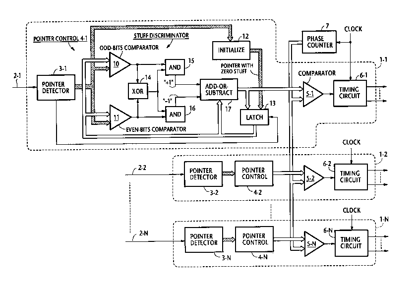
Referrlng now to Flg. 2, there ls shown a destuffing
clrcult accordlng to the present lnventlon. As lllustrated,
the destufflng clrcult ls made up of a plurality of llke unlts
l-i for recelvlng demultlplexed data slgnals whlch appear
respectlvely on lnput llnes 2-1 (where 1 ranges from 1 through
N). Each unlt 1-1 lncludes a polnter detector 3-i, a polnter
control circult 4-1, a colncldence detector or comparator 5-1
and a tlmlng clrcult 6-1, all of whlch are connected ln serles
to the assoclated lnput llne 2-1. Clock pulses that are
synchronlzed wlth the tlmeslots of the lncomlng TDM lnput are
applled to a slngle phase counter 7 to produce a blnary count
of the clock. Polnter detector 3-1 extracts a polnter from
each frame of the demultlplexed data slgnal lndlcatlng the
start tlmlng of the data slgnal of that frame and the type
(posltlve, negatlve or zero~ of destufflng to be performed on
that frame. Comparators 10, 11 and loglc clrcultry 14 to 15
comprlse the stuff dlscrlmlnator of unlt 1-1.
As wlll be descrlbed ln detall later, lf zero
destufflng ls to be performed on an Mth frame, the polnter
value "k" of thls frame ls a sequence of blts lndlcatlng the
0 start tlmlng of the data slgnal ln that frame. If posltlve
- 3a -
71024-191
NE-420 206697 1
- 4 -
destuffing is to be performed on an (M+1)th frame, the output of pointer
2 detector 3-i is a bit sequence in which the binary values of its odd-
3 numbered bits are opposite to those of the corresponding odd-numbered
4 bits of the Mth frame and one is added during the (M+1 )th frame to the
S pointer value of the Mth frame to produce a pointer value "k+1". If
6 negative destuffing is to be performed on an (M+3)th frame, the pointer of
7 this frame is a bit sequence in which the binary values of its even-
8 numbered bits are opposite to those of the corresponding even-numbered
9 bits of the (M+2)th frame and one is subtracted during the (M+4)th frame
10 from the pointer of the (M+2)th frame to produce a pointer value "k".
1 1 Returning to Fig. 1, each pointer control circuit 4-i includes an odd-bits
12 comparator 10 and an even-bits comparator 11, each having a first input
13 coupled to the output of pointer detector 3-i and a second input coupled
14 to the output of a latch 13. An initialization circuit 12 is connected to the15 output of pointer detector 3-i to store a zero-stuff pointer value initially
16 detected by pointer detector 3-i into latch 13. The outputs of comparators
17 10 and 11 are connected to an exclusive-OR gate 14 and AND gates 15, 16
18 to which the output of exclusive-OR gate 14 is also connected. A
19 destuffing circuit, or add-or-subtract circuit 17 is provided for receiving
20 add-one and subtract-one command signals respectively supplied from
2 1 AND gates 14 and 15 in order to add "+1 " or "_1 n to the pointer value of a22 previous frame that is stored in the latch 13 in response to a latch timing
23 signal from pointer detector 3-i. The pointer value modified by the add-
24 or-subtract circuit 1 7 is stored back into latch 13 to be used during the next
2 5 frame as a previous pointer. The output of add-or-subtract circuit 1 7 is
26 further applied to comparator 5-i. The comparators 10, 11, exclusive-OR
2 7 gate
28 Odd-bits comparator 10 produces a logic 1 when the odd-numbered
29 bits of the detected pointer are reversals of the corresponding odd-
3 0 numbered bits of the previous pointer, and even-bits comparator 11
NE-420 206697 1
produces a logic 1 when the even-numbered bits of the detected pointer
2 are reversals of the corresponding even-numbered bits of the previous
3 pointer.
4 The effect of exclusive-OR gate 12 and AND gates 1 3, 14 is to prevent
the unit 1-i from being adversely affected by a timing error which might
6 result in the simultaneous generation of logic-1 outputs from comparators
7 10 and 11. Therefore, AND gate 15 exclusively generates a logic 1 when
8 the output of odd-bits comparator 10 goes high, and AND gate 16
9 exclusively produces a logic 1 when the output of even-bits comparator 11
10 goes high. Add-or-subtract circuit 17 receives the logic-1 outputs of AND
1 1 gates 15 and 16 as add-one and subtract-one command signals, while
12 ignoring logic 0's from the AND gates.
13 Comparator S-i makes a comparison between the output of add-or-
14 subtract circuit 17 and the output of phase counter 7. If they match,
15 comparator 5-i supplies a coincidence signal indicating the start timing of a16 frame to timing circuit 6-i to which the clock pulse is also applied.
17 For a full understanding of the present invention, the operation of the
18 unit 1-i will be described with reference to Figs. 3 and 4.
19 Assume that during an Mth frame, pointer detector 3-i detects a
2 0 pointer value "k" (= 00011 11 1 11 ) and the same pointer value is stored in21 latch 13. These pointer values are compared with each other and a logic
22 0 iS produced by each of comparators 10, 11 and supplied to AND gates
23 15, 16. Exclusive-OR gate 14 also supplies a logic 0 to AND gates 15, 16.
24 Thus, each AND gate produces a logic 0, and hence add-or-subtract
2 5 circuit 17 passes the contents of latch 13 to its output terminal. The same
26 pointer value thus appears at the output of add-or-subtract circuit 17 and is27 stored back into latch 13 in response to a timing signal 20 from pointer
28 detector 3-i and applied to comparator 5-i.
29 During the (M+1 )th frame, the pointer value detected is a bit sequence
3 0 "1011010101 n which is representative of the value k with positive stuff.
NE-420 206697 1
- 6 -
Since the odd-numbered bits of this sequence are reversals of those of the
2 corresponding odd-numbered bits of pointer value "kn, odd-bits
3 comparator 10 produces a logic 1 and even-bits comparator 11 produces
4 a logic 0. Thus, exclusive-OR gate 14 produces a logic 1, and an add-one
S command signal is supplied to add-or-subtract circuit 17 in which a "1 n is
6 added to the value k stored in latch 13, producing a pointer value "k + 1 n
7 (= 0010000000) at the output of add-or-subtract circuit 17. The pointer
8 value "k + 1n is stored back into latch 13 in response to a timing signal 21
g and applied to comparator 5-i.
0 During the (M+2)th frame, the input data is a zero-stuff bit sequence
1 1 ~0Ol OOOOOOOR equal to the contents of latch 13, and pointer detector 13
12 detects a pointer value "k + 1". Both AND gates produce logic 0's and the
13 contents of latch 13 remain unchanged by latching the same k+1 value
14 again into latch 13 in response to a timing pulse 22.
15 During the (M+3)th frame, the input data contains a negative-stuff bit
16 sequence "0111010101 " having a pointer value "k+1". Since the even-
17 numbered bits are reversals of the corresponding even-numbered bits of a
18 zero-stuff k+1 pointer value, even-bits comparator 11 produces a logic 1
19 and AND gate 16 supplies a subtract-one command signal to add-or-
subtract circuit 17. The k+1 value from latch 13 is decremented by one
21 and a pointer value "k" (=0001111111 ) is stored back into latch 13 in
22 response to a timing pulse 23.
23 During the (M+4)th frame, the pointer value of the input data is a zero-
2 4 stuff bit sequence with a pointer value "k" (=0001 111 111), which is
2 5 compared with the same pointer value stored in latch 1 3, producing a
26 logic 0 at the output of each comparator 10, 11 . The pointer value stored
27 in latch 13 is again stored back in response to a timing signal 24 as a
28 reference for a subsequent frame.