Note: Descriptions are shown in the official language in which they were submitted.
~067~
OPTICALLY TRIGGERED H!(3H VOLTAGE SWITCH
N~TWORK AND METHOD FOR SWITCHING A HIGH VOLTA(:~
Technical ]~ield
The invention generally pertains to switches used to selectively convey
5 electrical current in respect to a hi~h voltage, and more particularly, to sn
electrically isolated, solid state switch network that is controlled by light signals
and to a method for switching an electrical current at a high voltage.
Background of the Invention
A common problem on electrical power distribution systems supplying power
10 to inductive loads is the need to provide reactive power compensation. Large
motors and other types of inductive loads used, for example, in lumber mills, rock
crushing plants, steel mills, and to drive elevators and pumps, shift the power
factor of the system away from the desired unity level, thereby decreasing the
efficiency of the power system. Compensation for the effects of inductive loads
can be provided to control line voltage, power factor, or volt-ampere-reactive
(YAR) power. Such compensation generally takes the form of capacitor banks that
are connected to transmission and distribution lines. While an appropriate
capacitive compensation can be determined and left on-line to compensate
continuously running inductive loads, most inductive loads operate intermittently
20 and cyclically, requiring that the correct compensation be selectiYely applied in
response to a varying reactive load on the system. Mechanical contactors are
typically employed to connect and switch the capacitor banks to compensate
changing inductive loads. However, mechanical contactors are known to introduce
undeslrable tr~nsients each time thsi they oper tte to change the reactive
2~75~7
--2-
compensation. Furthermore, being mechanical devices, mechanical contMctors
must be maintained, rebuilt, or even replaced after a limited number of operating
cycles.
Other devices have been developed for controlling reactive power at the
5 point of use, such as a power factor control system for induction motors developed
by Frank J. Nola, which is described in U.S. Patent No. 4,266,177. Unfortunately,
there are several problems with the Nola control system that have prevented it
from being widely used. For example, operational parameters of this type of
device must be tailored for use with a specific inductive load. In addition, thel0 Nola device can control power factor over only a limited range restricted to light
loads, since the device will not work at full loads. Three Nola devices are
reguired to control the power factor of a three-phase inductive load.
A reportedly transient-free, solid state automatic power factor correction
apparatus is disclosed in U.S. Patent No. 4,645,997. This apparatus is designed to
15 8utomatically correct power factor in a multi-phase system, on the load side of a
distribution trsnsformer, e.g., to correct the power factor of an inductive loadwithin a plant. It generates signals indicative of the voltage and current
associated with each phase supplying power to the load. The current and voltage
signals for each phase are compared to each other to determine the extent of
20 rurrent lag, and a signal ind-cative of current 18g iS generated for each line. A
microprocessor-controlled circuit converts these signals into a lagging phase angle
in degrees and determines the cosine of the ang!e and thus, the power factor of
the line. The microprocessor also controls a switching network that is capable of
selectively adding or removing banks of delta-connected cap~citors to or from the
25 power lines to control power factor. Only two silicon-controlled rectifiers (SCRs)
comprise the switching network for each bank of capPcitors. According to this
patent, the SCRs can connect the capacitor banks to the lines at any time,
regardless of the voltage on the capacitors, without creating current surges or
electrical transients. However, this device is intended to operate at relatively30 low distribution transformer secondary voltage levels typically used in 8 plant,
i.e., 480 volts or less, and it cannot accurately determine the required reactive
power compensation to control power fflctor if there are signiticant harmonics of
the fundamental 60 Hz line frequency present in the current or voltage, since such
harmonic distortion interferes with the measurernent of the phase angle or lag
35 time between voltage and currer t. In addition, the system disclosed in U.S.
Patent No. 4,645,997 lacks other features required for fully automated~
unattended operation, such as the capability for remote control of the switching
-3- 2~5~7
network and the ability to detec~ and compensate for malfunctions in the device.In any case, it is generally mo. e ef~ec~ive for an electric utility to provide
reactive power compensatiorl on the lines of an electric power distribution system
rather than depending on the customer 'o correct each load. The device disclosed5 in this patent cannot be used on dis.. ibution lines, because it cannot be controlled
remotely, cannot operate unattended. and cannot operate at the higher voltages
typically used on distribution lines (up to 35 1;~').
In U.S. Patent No. 4,6L~5,36 ~, ~vhich is issued to Williarrls and two of the
inventors of the present invention, a reacth,e power compensating system is
10 disclosed that is designed to directh. compensate an inductive load on multi-phase
lines of a distribution system. The appaIatus includes fixed capacitors that arealways connected to each phase or the systen- to provide a minimum reactive
power compensation, and selectivel~ switched capacitors that are connected to
each phase by a solid state switching network of SCR and diode pairs to provide
15 any additional compensation required. The required reactive power compensation
for all phases is determined in the devic~ b~ sensing the current on only one phase
at the time its voltage crosses zero.
The reactive power compensation system described in the Williams et al.
patent is deficient in several impor'ant respects. Since only one phase of a multi-
20 phase distribution system is used o determine the required reactive powercompensation for r~ll of the phases. the system cannot properly compensate for
di~ferent inductive demands on eac.A of the phases resulting, for example, from
various single phase and multi-phase nductive motors. Also, the determination ofthe required reactive power corr,r,ensa~ion is susceptible to errors caused by
25 harmonic distortion in the lin-- current and voltage -- a problem that is
specifically admitted in the paten'.. In some situations, use of a fixed capacitance
to provide a minimum required compe.nsation may be inappropriate, since, if all of
the significant inductive loads cor...ec'en to he system are at times de-energized,
the correct compensation ma~ be :nuc.h Iess than that provided by the fixed
30 capacitance. Furthermore, fault ~oler_nce and operation of the switching networlc
in the presence of voltage trar.sh:nts and harmonics are not addressed in this
reference.
In consideration of the above-no!ed problems that exist with the prior art
systems used to cornpensate for nc s~h,e !oads, a reactive power compensation
35 system is herein described that comDensates ~or different inductive loads on each
phase. It is an object of the preser.! nvention to provide a switch and a methodfor selectively connecting an approiA. ate c ar,acitance to provide the compensation
2~67~7
--4--
required ~or the inductive load on each phase of an electric~l power distribution
system. hlore generally, it is an object of the present invention to provide an
optically triggered solid state sv,litch and a method for selectively controlling the
flow of an electrical current at R high voltage without introducing transients or
5 harmonic distortion in that electrieal current. These and other objects and
advantages of the present invention will be apparent from the attached drawings
and from the Description of the Preferred Embodiments that follows.
Sum mary of the Invention
The present invention i9 an optically triggered solid state switch. One
10 embodiment of this switch includes energy storage means, connectable to a
voltage source, for conveying an electrical current and for storing an electrical
charge resulting frorn the electrical current. Transformer means are connected
generally in parallel with the energy storage means and are operative to produce a
trigger pulse in response to a pulse of electrical current flowing through the
15 transformer means from the electrical charge stored by the energy storage
means. Light sensitive means are connected generally between the energy storage
means and the transformer means and are operstive to controllably discharge the
electricsl charge stored by the energy storage means in response to a pulse oî
light, thereby producing the pulse of electrical current flowing through the
20 transformer rneans. Triggered s~itch means, which are connected to the
transformer means, provide a conductive path for an electrical current to flow in
respect to the voltage source, in response to the trigger pulse.
The voltage source can be a periodically varying potential. The optically
triggered solid state switch includes a trigger capacitor that is connected to the
25 energy storage means and is connectable to the voltage source. The trigger
capacitor charges to a peak potential o~ the voltage source as the electrical
current flows through the energy storage means.
The energy storage means comprise an energy storage capacitor that stores
the electrical charge, charging path means for conveying the electrical eurrent
30 that provides the electrical charge stored on the energy storage capacitor, and at
least one diode. The diode~s) is connected in series with the energy storage
capacitor so as to carry the electrical current in one direction.
The transformer means comprise a primary winding that is connected to the
energy storage means. and a secondary winding that is connected to the triggered35 switch means. The triggered switch means comprise a silicon controlled rectifier
and a diode connected in parallel with each other, the silicon controlled rectifier
having a gate that is connected to the transformer means to receive the trigger
~ X~75~7
pulse. In response to the tri~ger ?Ulse. the silicon controlled reetifier beginsconducting the electrical curren;. ~he diode is connected to carry an electricslcurrent in an opposite direction from the silicon controlled rectifier.
The light sensitive switch means comprise a phototransistor having a
c collector and an emitter connected to the energ~ storage means, and a transistor
controlled by the phototransistor. Thus. in response to the phototransistor, thetransistor conducts electrical current that flows through the transformer means
A plurality of optically triggered solid state switches are connectable in
series to the voltage source to provide tlle conductive path if the voltage source
exeeeds a peak voltage rating of a single optically triggered solid state s~itch.
The plurality of optically triggered solid state switches thereby are capable ofinterrupting the electrical current flow from the voltage source when the
triggered switch means stop conducting.
The optically triggered solid state switch can further comprise snubber
c means for protecting the triggered switch means from transient voltages in excess
of the peak voltage rating, and mezns for providing the light pulse to the lightsensitive switch means.
In one form of the invention~ ~he triggered switch means are connected to
provide the conductive path between a ground connection and a capacitor that is
connected to the voltage source.
A further aspect of this invention relates to a method for selectively
switching an electrical current at ~ ?eriodically var,ving high voltage. The steps
eomprising the method are generail; consistent with the functions of the elements
eomprising the optically triggered solid state switch described above.
Brief DescriDtion of the Drawings
.
FIGURE 1 is a schematic bloc!s diagram of a first embodirnent of the
reactive power compensator;
FIGURE 2 is an electrical cr,emalic diagram showing a comparator circuit
that is typical of those used in -~n 'nDut comparator block of the reactive power
compensator of FIGURE I;
FIGURE 3 is an electrical se.rematic diagram of a logic debounce circuit
that is typical of two such circuits in ~he first embodiment;
FIGUR~ ~A is an eleetricai ,chematic diagram of a timing logic circuit used
in the first embodiment of the reac~ive ?ower compensator;
FIGURE 4E3 is a diagram illust. ating the relationship between si~ voltage
waveforms that are used to produce ~iming signals in the first embodiment;
~ ~ 6 7 5 ~ ~
I
-6
FICIJRE 5 is an electrical schematic diagram of a TTL/MOS match and
amplifier (TMMA) circuit;
FIGURE 6 schematically illustrates an analog amplifier circuit used to
buffer and/or amplify signals in a signal-conditioning block of the present
5 invention;
FIGURE 7 is A graph showing several cycles of a potential signal and a cycle
of a distorted current signal, illustrating the effect of harmonic distortion on the
determination of the reactive power compensation required for each phase;
FIGURE 8 is an electrical schematic diagram of a typical dual filter circuit
10 used to filter out harmonic distortion;
FIGURE 9 is a graph illustrating harmonic distortion in the voltage
wsveform on one phase;
FIGURE 10 is an electrical schematic diagram of a window circuit used in
controlling connection of the reactive power compensation capacitance;
FIGURE 11 is a schematic block diagram showing a first embodiment of a
switch driver;
FIGURE 12 is an electrical schematic of a triggering bridge and pulse
transformer circuit used in the switch driver of FIGURE 11;
FIGURE 13 is a block diagram of a compensation capacitor array for one
20 phase;
FIGURE 1~ is an electrical schematic diagram of a network of optically
triggered switch drivers and solid state switches for one compensation capacitoron one phase;
FIGVRE 15 is a graph illustrating control and data acquisition intervals for
25 several cycles of the three-phase voltage waveforms;
FIGURE 16A is a flow chart ilIustrating a main program loop;
FIGURE 16B is a flow chart illustrating the control logic used by a personal
computer ~PC~ in determining and controlling the connection of an appropriate
reactive power compensation capacitance to each line of 8 multi-phase system;
FIGURE 16C is a flow chart illustrating the details o~ the data acquisition
logic implemented in the main program of FIGURE 16A;
FIGURES 17A, 17B, and 17C are electrical schematic block diagrams of a
second embodiment of the reactive power compensator for one phase ~A~);
FIGURE 18 is an electrical schematic diagram of the trigger and logic
35 circuit and optical driver and transmitter of the second embodiment shown in
FIGURES 17A, 17B~ and 17C;
~6~
7-
FICURE 19 i9 an electrical scnematic diagram of the watchdog timer circuit
noted in FIGURE 17E~;
FIGURF 20A is a flow char~ of the main program implemented by the
controller of the second embodiment shown in FIGVRE 17E3; and
FIGURE 20B is a flow chart of the logic implemented by the eontroller in
determining and controlling the connection of the appropriate reactive power
compensation capacitance for one phase.
DescriDtion of the Preterred Embodiments
PC Controlled R aetivc Power ComDensator
Referring to FIGURE 1, a first embodiment of the reactive power
eompensator is shown generall~ at reference numeral 50. In the application of the
present invention illustrated therein, reactive power compensator 50 determines
an appropriate eompensation capacitor to apply to lines 52a, 52b, and 52c, whichare conneeted to one or more inductive loads (not shown). Lines 52 carry
three-phase electrieal eurrent frorn a remote generator or other three-phase
source (not shown). The voltage on lines 52 is monitored by corresponding voltage
transformers (VTs) 54. Similarlv, current transformers (CT's) 58 are used to
monitor the eleetrieal eurrent flo-. ing from the source to each load through
lines 52. Reaetive power compensator 50 separately monitors the voltage and
eurrent on eaeh phase and separate!v determines an appropriate capacitance to
eompensate for the inductive loaa(sj connected to each phase, whieh may differ
between the phases. Compensation capacitors 112 are electrically conneeted to
eaeh line 52 via lines S~. These capacitors can selectively be connected to neutral
or ground via solid state s~vitcning circuits 11~ to provide reaetive power
eompensation. Reaetive power compensator 50 ean seleetively be operated in a
manual mode in which a locai or rernote operator determines the speeific
eompensation eapaeitors that are connected to provide compensation on lines 52,
or it can be operated in an automatic mode in which the reactive power
eompensator determines the spec- c compensation eapaeitors that must be
connected to achieve a user-se!enred or predetermined volt-ampere-reaetive
(VAR~ level on the line. Alterna~ivelv, resetive power eompensator S0 csn
selectively be used to automat!callv maintain a predetermined voltage, or a
predetermined power factor (PF) on each line 52, or ean provide reaetive power
compensation or predetermined line ;oltage based upon a time sehedule.
The mode in which reactive ?ower eornpensator 50 operates is seleetively
determined by the operator Of the device by commands entered in a local personaleomputer (PC) eontroller 70. In addition, local PC controller 70 ean optionally
~6~57
--8--
monitor, record, and display data corresponding to the output signals frorn
convent;onal watt, VAR, snd power factor (PF) transducer within an
instrumentation bank 78, which are carried on data leads 79. These signals are not
used ~or determining the reactive power compensation, but can be provided by
transducers that use the same voltage and current signals required by the reactive
power compensator. For example, as sho~n in FIGURE 1, c~rS 58a, 58b, and 58c,
are connected to monitor the electric current ~lowing in lines 52a, 5~b, and 52c,
respectively, producing secondary current signals on leads fiOa, 60b, and 60c,
which are indicative of the actual current in lines 52. Transducer instrurnentation
bank 78 is connected to leads 60. Thus, secondary current from CTs 58 flows
through each transducer requiring a secondary current signal indicative of electric
current flowing in lines 52, and on into leads 61 ~or use in determining the
required reactive power compensation. Likewise, potential signals from voltage
transformers 54 are connected to transducer instrumentation bank 78. Signals
from these current and voltage transformers are used by reactive power
compensator 50 for determining the appropriate reactive power compensation as
described below.
An optional remote PC controller 72 can be connected to local PC
controller 70 by a communications link 7Js to control reactive power
compensator 50 from the location where remote PC controller 72 is installed. Forexample, electric Itilities often provide a central control facility for their
distribution system from which an operator can monitor and control the equipmentconnected to the distribution lines. Remote PC controller 72 may thus comprise arelatively large computer that controls power switches and other devices.
Reactive power compensator 50 includes a synchronization block 62 in which
timing signals are derived from the potential signals supplied by voltage
transformers 54 for use in controlling the reactive power compensator. Signals
indicative of the current and the potential on lines 52 are amplified and filtered in
a conditioning block 64. I,ocal PC controller 70 uses the timing signals and thesignals indicative of current and potential on lines 52 to determine an appropriate
reactive power compensation for each line 52 and produces control signals that
are supplied to a plurality of triggering blocks 6S. Triggering blocks 66 respond to
the control signals in developing triggering signals that are input to a plurality of
switching blocks 68 and cause an appropriate reactive power compensation
capacitance to be connected to each line 52. Only one trig~ering block 66 and one
switching block 68 are shown in FIGURE 1.
2 0 ~
g
Voltage transformers ~ include primary windings 54H, 54b, and 54c,
respectively, each of wnich are connected between the corresponding
line 52a, 52b, and 52c and ground. These voltage transformers include secondary
windings 5~a', 54b', and 54c', which are, -espectively, connected to leads 76a, 76b,
5 and 76c. A signal corresponding to the voltage on each of lines 52 is thus supplied
to transducer instrumentation bank 78 and to Delta-Wye and ~elta-Delta
transformer banks 80. At rated voltage on lines 52, the potential signal supplied
through leads 76 is nominally 120 'I .~C. Delta-Wye and Delta-Delta transformer
bsnks 80 comprise either two three-phase voltage transformer banks or six voltage
10 transformers connected in Delta-Wye and Delta-Delta configurations, producing a
relatively low voltage output signal (less than 20 V AC) that is conveyed over
leads 81 to an input comparator circuit ~2 and an analog amplifier circuit 90. The
six potential signals produced by Delta-Wye and Delta-Delta transformer banks 80respectively correspond to the line-to-neutral periodic sinusoidal voltage
lS waveforms on A phase (line 52a), B phase (line 52b), and C phase (line 52c), and to
the line-to-line voltages AB, BC, and CA.
FIGURE 2 illustrates a comparator 118a that is used in the input comparator
circuit 82. This circuit is typical Ot the six comparator circuits supplied potential
signals from Delta-Wye and Delta-Delta transformer banks 8D. As shown in
20 FICURE 2, an input potentiai signal on lead 81 is applied to two resistors 120
and 122, which are connected in series by a conductor 121. Resistor 122 is
connected to ground so that the t wo r esistors divide the voltage of the input
signal, producing a lower level potential signal that is applied by conductor 121 to
the inverting input of a comparator 124. The non-inverting input of
25 comparator 124 is connected ;o ground through a lead 123 and the comparator
output is connected by a lead 125 to the anode of a diode 128 and to one end of a
resistor 126. The opposite end of resistor 126 is connected to ~5 V DC. A
lead 129 is connected to the cathoae ot diode 128 and is referenced to ground via
a resistor 130. The sinusoidal potentiai signal applied to the inverting input of
30 comparator 124 produces a corresponb ng square wave ranging between -S volts
and +5 volts in amplitude. However. due to the ~5 V DC level applied through
resistor 126 and diode 128, the output signal on lead 129 is a square wave ranging
between approximately 0 volts and -~ volts.
Referring back to FIGI~E~E 1, the six square wave signals produced by input
35 comparator circuit 82 are conve~ed through leads 83 to A logic debounce
circuit 84 that cleans up any ,itter or noise present on their leading and trailing
edges, which can occur at each zero crossing of the potential signal input to
2~7~
-10-
comparator 124. Details of a debounce circuit 132, which is typicaJ of the two
such circuits comprising logic debounce circuit 84, are shown in FIGURE 3.
Turning now to FIGURE 3, three leads 129a, 129b, and 129c, respectively
carry square wave signals (possibly having noise on their leading and trailing
5 edges) that correspond to the voltage waveforms on A phase, B ph~se, and
C phase. Thus the square waves are at ~5 V DC during the positive half cycle of
the voltage waveforms and at zero during the negative half cycles. Lead 129a is
connected to one of two inputs of NAND gates 134a and 134b and to or,e of two
inputs of OR gates 136a and 136b. Similarly, lead 129b is connected to orne input
10 Of NAND gates 134b and 134c and to one input of OR gates 136b and 136c; and
lead 129c is connected to the other input of NAND gates 134a and 134c and to theother input of OR gates 136a and 136c. Debounce circuit 132 also includes three
D flip flops 138B, 138b, and 138c that have their D and clock inputs grounded.
Each of NAND gates 134a, 134b, and 134c are connected by leads 135a, 135b,
15 and 135c to the inverted preset input of the three D flip flops, respectively.
Likewise, the outputs of OR gates 136a, 136b, and 136c are connected to the
inverted clear inputs of the D flip flops via leads 137a, 137b, and 137c,
respectively.
A logic level 0 applied to the inverted preset inputs of the D flip flops causes20 their Q output to have a logic level 1, and a logic level û on the inverted clear
input causes the Q output to have a logic level 0 value. Elimination of any jitter
present on the leading and trailing edges of the square wave signals earried on
leads 129 occurs as follows. When the incoming square wave signal on lead 129a
(A phase) first rises to a logic level 1 (at the leading edge of the square wave) the
25 square wave signal on lead 129c (C phase) will already be at a logic level 1. A
logic level 0 is thus output from NAND gate 134a and is applied to the inverted
preset of D flip flop 138a, causing its Q output to lock at a logic level 1 snd its
Q output to lock at a logic level 0. The square wave signal on lead 129c ~C phase)
then drops to a logic level 0. The first time that the square wave signal on
30 lead l~9a drops to zero (the trailing edge of the square wave signal) OR gate 138a
will produce a logic level 0 output, causing the Q output of D flip flop 138a to lock
at logic level 0. D flip flops 138b and 138c operate in a similar manner to provide
clean digital signals (square wave signals) corresponding to one half period of the
potential signal on B phase and C phase, respectively. Although not shown in
35 FIGURE 3, a second debounce circuit of identical design is used to eliminate jitter
at the leading and trailing edges of the square wave signals corresponding to AB,
BC, and CA potential signals.
2 0 6 7 ~ 5 7
-- , 1 --
The Q and Q logic level signals output frorn logic debounce circuits 84 are
conveyed through leads 140 and 1~1 (collectively, leads 85) to a timing waveformlogic circuit 86 (see FICURE 1), which is shown in detail in FIGURE 4A. Tirning
waveform logic circuit 86 includes 15 ~AND g~tes 148a through 148O, each of
which have two inputs that are connected to leads 140 and 141 on which are
respectively conveyed the Q and q square wave signals output from logic
debounce circuit 84. Specificall~, the signal on lead 140a is connected to one
input of NAND gate 148e, 148g, and 1~81. The Q, or inverted. version of this
signal is conveyed on a lead 141a to one input of NAND gate 148m The signal for
10 E~ phase (the Q output) is conveyed by a lead 140b to one input of NANI)
gates 148d, 148f, 148h, and 148j. The inverted form of this signa] is conveyed by a
lead 141b to NAND gate 148n. For C phase, the signal on lead 140c is connected
to NAND gates 148d, 148i, and 1~ k. The inverted form of this signal is conveyedby a lead 141c to NAND gate 148O. For -~8 phases, a lead 140d conveys the signal15 from the debounce circuit to NAND gates 148a, 148h, and 148m. The
corresponding inverted signal is conve~ed by a lead 141d to NAND gate 1481. The
signal on lead 140e for BC phases is input to NAND gates 148b, 148i7 and 148n.
The inverted form of this signal is applied via a lead 141e to IJAND gate 148j. A
lead 140f conveys the signal for CA ?hases to NAND gates 148a, 148c, 148g,
20 and 148O. The inverted form oî this signal is applied through a lead 141f to
NAND gate 148k.
Leads 150a through 150O car.; the signals output from NAND gates 148a
through 148O, respectively. As illustrated in FIGURE 4B, these signals comprise
logic levels that change from low to high during intervals that extend over
25 integral numbers of 30 increments! eg., for 30, 60, 90, etc., of a 60 Hz
waveform. In FIGURE 4E~, the normalized voltage waveforms corresponding to
the six potential signals are shown in respect to the inverted logic level for the
signals on leads 150a through 150O. Rather than showing the actual form of thesesignals on leads 150, FIGURE 1B iilustrates the signals after they go through an30 additional stage of inversion. Nnicn occurs in a TMMA circuit 88 (FIGURE 1).
These signals are used for timing, ?.g.! to define time intervals around the zero
crossing for each of the three-pnase voltage waveforms and around the negative
peak of those waveforms. For example. the timing signals shown in the first three
lines of FIGURE 4B define a ~0~ inter-al centered about the point at which the
35 voltage waveform for each of the ~hree ?hases crosses zero. The period occurring
30 prior to the zero crossing for .~ pnase is identified as I'lam1" and the 30interval that immediately follows s identified as "lam2 " In this notation, the "I"
2 0 6 7 ~ 5 ~
--12--
refers to current, "a" refers to A phase, and "m1" and "m2" respectively refer to
the first and second periods associated with multiplexed current rneasurements
preceding ~nd following the voltage waveform zero crossover point.
The timing signals on leads 150d, 150e, and 150f define 60 intervals
5 centered around the negative peaks of each of the voltRge waveforms for
the A, B, and C phases. The notation identifies these three signals as multiplexed
measurements of voltage occurring in a first and second interval centered about
the negative peak of each of the illustrated three-phase voltage waveforms. For
example, the signal on lead 150d is referred to as "Vam1 ~ Vam2," the "V"
10 identifying a voltage measurement; the other terms in the notation have already
been explained.
The signals on leads 150g, 150h, and 150i represent 30 intervals occurring
immediately before the negative peak for the three-phase voltage
waveforms ~, C, and A, respectively. These timing signals are referred to by
15 notstion indicating that they ar~e used to control sampling of the voltage on each
phase. Similarly, the signal on leads 150m, 150n, and 150O identify 30 time
intervals occurring 30 before each of the zero voltage crossovers for A, B, andC phases, respectively. The notation used with each of these three signals
indicates that they are used in connection with sampling current on each of the
20 three phases. For example, the signal on lead 150m is identified with the notation
~la5~ wherein "1" indicates a current measurement, "a" indicates A phase~ and "s"
indicates a sample and hold timing signal.
The signals on leads 150 (collectively shown in FIGURE 1 as leads 87) are
input to TMMA circuit 88, details of which are shown in FIGURE 5. TMMA
25 circuit 88 includes eight comparators 152a through 152h. Leads 150a through 150f
are connected to the inverting input of comparators 152a through 152f,
respectively. The non-inverting input of each of these comparators is connected
by a lead 164 to the common node between two series-connected, equal value
resistors 160 and 162. Resistors 160 and 162 are connected between +5 V DC and
30 ground so that their common node to which lead 164 is attached is at a potential
of approximately 2.5 V DC.
Leads 150g through 150i are connected to the three inputs of a
NAND gate 154, the output of which is connected to the non-inverting input of a
comparator 152g through a lead 156. Similarly, leads 150m through 153O are
35 connected to the three inputs of a NAND gate 158 that has an output connected to
the non-inverting input of a comparator 152h- The inverting inputs of
comparators 152g and 152h are connected to the 2.5 V DC potential on lead 164.
2~7~
- 13-
The outputs of compar~tors 152a through 152h connect to leads 166a
through 166h, respectively, and are thus connected to one end of pulJ-up
resistors 168a through 168h, the opposite ends of which connect to +5 V DC.
Accordingly, comparators 152a through 152h convert the lo~ic level signals at
5 their inputs, which range between 0 and 5 V DC, to signals that range between -5
and +5 V DC. Since NAND gate 154 and NAND gate 158 invert the logic sense of
the timing signals respectively applied to their inputs, the output of these
NAND gates are connected to the non-inverting input of comparators 152g
and 152h for comparison against 2.5 V DC. The signals output from
10 comparators 152g and 152h are supplied on leads 166g and 166h to a sample and hold circuit 96. As shown in FIGURE 1, lesds 166 comprise leads ~9.
The timing signal output on lead 166g includes three 30 pulses used to
control the sample and hold ol` potential signals for the three phases, i.e., todetermine when to hold a value corresponding to the negative peak voltage on
15 each of the three phases A, B~ and C. Similarly, the three pulses comprising the
timing signal output from com~arator 152h on lead 166h is used to determine the
time at which current is to be rneasured for each of the three phases, where that
time corresponds to the zero crossing of the corresponding potential waveform for
esch line 52. The signals on leads 166a through 166f are input to a multiplexer 94
20 (see FIGURE 13 over leads 89 to control the selection of signals indicative of
current and potential on each of the three phases A, B, and C, so that the
appropriate signal is output from multiple.Yer 94 to sample and hold circuit 96 via
lesds 95. The timing signals appiied to multiplexer 94 from TMMA circuit 88
cause the selected potential or current signal ~rom the multiplexer's input signals
25 to be output from the multiple:~er over leads 95 starting 30 before the negative
peak voltage occurs, and 30 be~^ore the zero voltage crossing of the voltage
waveform, respectively. Thus, the appropriate multiplexed potential or current
signal is applied to sample and hoid circuit 96 well ahead of the point in time at
which a value sampled is to be heid and supplied to local PC controller 70 over a
30 lead 97. Oetails of the multiple~er and of the sample and hold circuit are not
shown, since they are generally conventional and sre well known to those of
ordinary skill in this art.
Before the signals indicati~e of current and voltage on each of the three
phases (lines 52) are supplied to ~ultiole~er 94 and then to sample and hold
35 circuit 96, as shown in FIGURE 1, these signals first pass through analog amplifier
circuit 9û. Signals from the analog amplifier circuit are conveyed via leads 91 to
a dynamic filter 92, which filters out harmonic distortion.
~7~7
Details of analog amplifier circuit 90 are shown in FIGURE 6. The
secondary currents from current transformers 58a, 58b, and 58c flow through
leads 61a, 61b, and 61c, respectively, to shunt resistors 171a, 171b, and 171c.
These shunt resistors are relatively low-va]ued resistors that are connected to
ground. The potential developed across the shunt resistors is conveyed through
input resistors 170a, 170b, and 170c, respectively, to the inverting input of
operations amplifiers (OP amps) 172a, 172b, and 172c; the non-inverting inputs of
these OP amps are connected through resistors 178a, 178b, and 178c to ground.
Feedback resistors 176a, 176b, and 176c determine the gain of OP arnps 172a
through 172c (in respect to the resistance of input resistors 170). Op amps 172
thus produce amplified current signals corresponding to the electrical currents on
each of A, B, and C phases (lines 52), and these current s;gnals are carried on
leads 174a, 174b, ~nd 174c.
Similarly, leads 117a, 117b, and 117c each conduct a feedback signal
indicative of the charge current for the compensation capacitors 112 connected to
the three phases, which represents the reactive power compensation actually
being provided to esch phase. These feedback signals are applied Rcross shunt
resistors 181a, 181b, and 181c, respectively. The potential developed across these
three shunt resistors are applied to the inverting input of OP amps 182a, 182b,
and 182c through input resistors 180a, 180b, and 180c, respectively. The
non-inverting inputs of OP amps 18Z are connected to ground through
resistors 188a, 188b, and 188c. Feedback resistors 186a, 186b, and 186c provide a
desired gain. The amplified feedback signals from OP amps 182 are carried on
leads 184a, 184b, and 184c.
The three signals indicative of the voltage on A, B, and C phases developed
by voltage transformer secondary windings 54a', 54b', and 54c', are supplied
through leads 81a, 81b, and 81c to the non-inverting inputs of OP amps 192a, 192b,
and 192c through input resistors 190a, l90b, and 190c. The non-inverting inputs of
the OP amps are referenced to ground through resistors 194a, 194b, and 194c.
Feedback resistors 198a, 198b, and 198c connect output leads 196a, 196b, and 196c
of these OP amps back to their inverting input. - OP amps 192 are thus configured
to buffer the potential signals developed by the three voltage transformers
connected to the distribution lines. Leads 174, 184, and 196 collectively comprise
leads 91, which convey the buffered potential signals to dynamic filter 92.
In determining the required reactive power compensationj or power factor
for each phase, the current flowing through each of lines 52 is measured when the
potential on that line crosses zero. Any harmonic distortion in the current flowing
20~7~7
, 5
in each of the lines 52 is reflec~ed in the current si~nals, which are output from
amplifier circuit 90. Such distortion can introduce an error in the determination
of the required reactive powe~ compensation or power factor for each phase as
shown in FIGURE 7. In this Figure, the potential and current for a single phase
5 are shown. As will be apparent from this iliustration, the instantaneous value of
current in the distorted waveform when the potential waveform crosses zero can
be substantially greater or less than the actual value for current at the
fundamental frequency, which is represented by a dashed line in this Figure.
Distortion of the potential signal indicative of voltage on each phase can have a
10 similar effect on accuracy. ~ccordingly, it is important to filter the signals
indicative of current and potential on each phase to eliminate the efEect of
harmonic distortion, so that the requirecl reactive power compensation can be
accurately determined.
FIGURl~ 8 illustrates part of the circuit used in dynamic filter 92 to
15 substantially eliminate any harmonic distortion on the current and potential
signals output from amplifier circuit 90. The signals indicative of current flowing
on A phase and B phase are conve~,ed via leads 174a and 174b, respectively, which
are connected to input resistors 200a and 200b. These two resistors are connected
to the two inputs of a dual bandpass filter 212, which is one of five such filters
20 - used in the dynamic filter. The other dual bandpass filters are configured
generally as shown in FIGURE 3 and are used to filter the remaining current and
potential signals for each phase.
In the preferred embodiment, a ~lotorola~ type MFlOCCN switched
capacitor filter integrated circuit is used for dual bandpass filter 212; however,
25 other filter circuits could be used for this purpose. The "Q" and other
characteristics of each section of dual bandpass filter 212 are determined by
resistor networks comprising resistors 204a/204b and 204c/204d. One end of
resistors 204a and 204b is connected to one side of resistor 200a via a lead 202a,
and their opposite ends are connected to the first section of dual bandpass
30 filter 212. Resistors 204c and 2~d are similarly connected to resistor 200b via
lead 202b and to the second fiiter section. Switched capacitance filters, such as
dual bandpass filter 212, require that a reference signal be supplied having a
frequency equal to 100 times the center frequency of the pass band. Each sectionof the dual bandpass filter is therefore provided with a 6 k~z reference frequency
35 signal over a lesd 208, preferabh~ ~rom a phase-locked loop circuit 206. The
phase-locked loop circuit is synchronized to the 60 Hz line frequency of lines 52
and thus tracks line frequency fluctuations on the lines.
21~67~7
The fllter~d output signals from dual bandpass filter 212 are input to
multiple.Yer 94 over leads 210a and 210b; collectivelyJ all of the output signals
from dynamic filter 92 are input to multiplexer 94 over leads 93. Due to the useof dynamic filter 92, reactive power compensator 50 is substantially llnaffected by
5 harmonic distortion present on the current and potential on lines 52, and
therefore, can more accurately determine the reactive power compensation
required on each phase and by monitor;ng the filtered feedback signals, can
determine if the compensation capacitors 112 are operating properly to provide
the expected compensation.
The timing signals supplied multiplexer 94 from TMMA circuit 88 over
leads 89 causes the multiplexer to select one of the filtered current and potential
signals at its input for sampling 30 before that signal is to be sampled and held by
sample and hold circuit g6. In addition, the timing signals applied to sample and
hold circuit 96, also over leads 89, define the time at which the selected
15 multiplexed signal output by multiplexer 94 is sampled and supplied to local PC
controller 70 over leads 97. The local PC controller includes a plug-in card (not
shown~ that performs an 8-bit analog-to-digital (AD) conversion of esch signal
supplied by sample and hold circuit 96, enabling a local PC controller to compute
the required reactive power compensation for each phase, based upon the
20 magnitude of the line current at the time the potential signal on that phase
crosses zero. Since timing signals for this operation are all supplied by TMMA
circuit 88, local PC controller 70 need only determine the appropriate
compensation capacitor(s) that must be connected to each of the respective
iines 52 to provide the computed compensation and supply the control signals that
25 effect connection of those selected compensation capacitors to the lines.
Compensation capacitors 112 are only connected to compensate one of
lines 52 when the potential on the line reaches a peak value. The control signals
for selecting specific compensation capacitors that are connected at this time are
supplied by local PC controller 70 over leads 101 to an optical transmitter 100,30 which comprises part of triggering block 66. The timing signals that determine
when the compensation capacitors selected by local PC controller 70 are
connected to each of the lines 52 (preferably at the negative peak voltages so that
initial current flow through switch circuits 114 is zero as the switch circuits are
first turned on) are supplied to optical transmitter 100 by the timing waveform
35 logic circuit 86 over leads 87.
Connection of each of the compensation capacitors 112 to lines 52 is
effected as described below"Jsing switch circuit 114, which comprises pairs of
- 17- 2 ~
silicon-controlled rectifiers (SC Rs) and diodes, as shown schematically in
FIGURE 1. Once Fated into conduction, the Sc~9 continue to carry charge
current to the capacitor so long as the direction of current flow through the SC~s
does not change. However, transient and/or harmonic distortion in the voltage on5 each of lines 52 can cause the SCRs to briefly conduct charge current to the
compensation capacitors, but to prematurely stop conducting in response to a
reverse bias voltage across the SCRs due to system voltage harmonics. This
condition is illustrated in FIGURE 9. As the distorted potential signal reaches the
nominal negative peak, the SCRs are gated on to enable the flow of charge
10 current in respect to a compensation capacitor 112; however, when the potential
decreases from its nominal peak value, the SCRs turn off, prematurely
disconnecting the compensation capacitor prematurely erom the line. To prevent
this condition, a window circuit 98 is included in triggering block 66 for each
phase, as shown in FIGURE 1. Window circuit 98 receives an inverted and filtered15 potential signal indicative of the voltage on one of the phases from dynamic
filter 92 through lead 93. Using his potential signal, a "window pulse" signal is
produced that insures proper operation of switch circuits 114. (The output of
window circuit 98 comprises a puise that is 30 in width and is referred to as awindow pulse signal.) The window ?Ulse signal starts just before the negative peak
20 voltages on lines 52.
The components of window circuit 98 for one of the phases are shown in
FIGURE 10. At the input of the wi aow circuit, lead 93 is connected to the anodeof a diode 213, to one side of a ?otentiometer 219, and to a resistor 222. The
signal on lead 93 is half wave rect,fied by diode 213, and the cathode of the diode
25 is referenced to ground through resistors 214 and 216- These resistors serve to
divide the rectified voltage to an ntermediate level, which is applied through alead 215 to the inverting input oî a comparator 217. A capacitor 220, which is
connected between lead 215 and ~-ound. filters the rectified signal, yielding a
positive DC level that is compared ~o the sinusoidal voltage set by the wiper of30 potentiometer 219 and applied G he non-inverting input of the comparator
through a lead 218.
Resistor 222 is connected to ~ 9û phase shift circuit 223 that comprises two
capacitors 223b and 223c, which are connected at each end of a resistor 223a to
ground. The 90 phase shifted sinusoidal waveform output from phase shift
35 circuit 223 is applied to the non-in~.erting input of a comparator 224; the inverting
input is connected to the wiper of 9 potentiometer 225, which is connected
between the ~5 V DC and -5 V DC supplies (not shown). The potentiometer wiper
2~6~ ~r~
provides an adjustable reference voltage, to corltrol a square wave signal on the
output of comparator 224. A lead 221 connects the output signals from
comparators 217 and 224 together, so that they are summed, producing a logical
AND signal that is applied to an output buffer 227. This summed signal is
connected to +5 V DC by a resistor 226. Potentiometer 219 is adjusted to vary the
width of the square wave signal output from comparator 2179 potentiometer 225 isadjusted to vary the start point for the phase-shifted square wave and thus the
width of signal produced by combining the output of comparators 224 and 217.
Accordingly, a 30 window signal is achieved and supplied to output buffer 227.
10 The output buffer comprises a comparator 227a having its output connected to
+5 volts through two series-connected resistors 227b and 227c. The voltage
division provided by these two resistors serves to convert the 30 window pulse
from a signal that varies between -5 volts and ~5 volts to a signal that varies from
0 to +5 volts. The 30 window pulse is output on a lead 99, which is connected to
15 the common node of resistors 227b and 227c.
Optical transmitter 100 comprises a plurality of light emitting diodes (not
shown) that respond to control signals from local PC controller to produce lightsignals used for selecting the specific reactive power compensating capacitors
that sre to be connected to each phsse. These light signals are produced by
20 - combining the timing signal provided by timing waveform logic circuit 86 over
leads 87, for each phase with the control signals from local PC controller 70 over
leads 101 and with the 30 s~indow pulse signal from window circuit 98 over
leads 99 in an AND gate (not shown). Optical fibers lD2 carrying the light signals
provide complete electrical isolation from high line voltage that could destroy the
25 components of reactive power compensator 50 that are electrically connected to
optical transmitter 100.
In the event that the length of optical fibers 102 required to transmit light
signals to switching block 68 causes excessive attenuation of the light signals
propagated therethrough, an optional buffer amp (not shown) can be provided to
30 amplify the intensity of the light signals~ producing corresponding light signals at
its output that are conveyed through the optical fibers 102 to a switch driver 110
in switching block 68, as shown in FIGURE 1. Typically, the buffer amp is not
required if optical fibers 102 are less than a few hundred feet in length.
FIGURE 11 shows only a portion of switch driver 110 used to develop the
35 signsls for switching a single compensation capacitor 112. The circuit illustrated
in FIGURE 11 is typical of other such circuits comprising reactive power
compensator 50, each of which is used ~or one of the compensation capacitors
2 0 ~ 7
-19-
provided for connection to each line 52. Not shown in FIGURE 11 are the light
sensors included within optical receiver 104 that convert the light signsls
propa~ating throughout optical fibers 102 into corresponding electrical pulses.
The light pulse conveyed by one of optical fibers 102 is converted to a
5 corresponding electrical pulse by a light sensor in optical receiver 104, and this
electrical pulse is input to an AND gste 228, the other input of which is connected
to receive 10 kHz pulses produced by 10 kHz generator 108 and conveyed over
leads 109. AND gate 228 carries out a logical AND operution t~ combine these
two input signals, producing a 30 window of 10 kHz pulses on its output lead 229,
10 which is connected to a triggering bridge and pulse transformer 230.
Triggering bridge and pulse transformer circuit 230 produces n trig~ering
signals that are conveyed over leads 1111 through leads 111n to a corresponding
number of rectifier circuits 232, i.e., to rectifier circuits 2321 through 232n. The
number of triggering signals and rectifier circuits needed depends upon the
15 number of SCRs which are required to selectively connect and disconnect each
compensation capacitor 112 to provide reactive power compensation for one of
lines 52, which in turn depends on the voltage on those lines. Rectifier
circuits 232 bloclc the negative portion of the 10 kHz pulses contained in the 30
window output from triggering bridge and pulse transformer 230, producing a 30
20 window that contains only positive ~ kHz triggering pulses on leads 111.
Details of triggering brige and pulse transformer 230 are shown in
FIGURE 12. Output lead 229, whicn is carr~ ing the 30 window of 10 kl~z pulses,is connected on both sides of the triggering bridge and pulse transformer circuit,
sp2cifically to resistors 234a and 234b. These resistors are connected to the gate
25 of two field effect transistors (FETs) 236a and 236b. The drains of each of the
FETs 236 are connected to ground ;ia lead 238. The anode of a diode 240 is also
connected to ground and its cathode is connected throu~h a lead 242 to the
collector of a PNP transistor 2~4. :Yhicn has an emitter connected to 170 V DC via
a lead 246. The 170 V DC is also connected to the source of FET 236a through a
30 resistor 248 and a resistor 250. These two resistors are connected in series and
their common node is connected :o the base of PNP transistor 244. In addition,
the 170 V DC is connected to the cathode of a diode 252, the anode of which is
connected to the source o~ FET '3fib. .-~ lead 254 connects the source of FET 236b
to one end of a primary winding ''58 of a pulse transformer 256. The other end of
35 the pulse transformer is connected to lead 242, and thus to the collector of PNP
transistor 244 and the cathode of diode 240. A pluralit~ of secondary
windings 2601 through 260n are connected between leads 2611/262l
-2~- 2~7~5~
through 261n/262rl, respectively. Each pair of these leads comprises one of the
leads lll thus carries an envelope of 10 kHz pulses within a 30 window that areused to selectively connect one of the compensation capacitors 112 to provide
compensation for one of lines 52. If transient or harmonic distortion in the
5 voltage waveform reverse binses the SCRs, prematurely stopping current flow
charging compensation capacitor 112, a successive 10 kHz pulse in the envelope
immediately retriggers the SCRs so that charge current again flows.
Operation of triggering bridge and pulse transformer 230 is relatively
straightforward. The 10 kHz pulses in the 30 window, which are applied to the
10 gates of FETs 236a and 236b cause the FETs to conduct current. Current flow
through resistors 248 and 250 produces a bias signal on the base of PNP
transistor 244, causing it to conduct. Current thus flows from the 170 V DC
through PNP transistor 244 and through primary winding 258 of pulse
transformer 256, continuing on to ground through FET 236b. The resulting 10 kHz
15 pulsating current flow through the primary winding of the pulse transformer
causes a corresponding current in its secondary windings 2601 through 260n. Eachtime that FETs 236a and 236b turn off, diodes 240 and 252 dissipate residual
inductive current flowing within primary winding 258.
FIGURE 13 illustrates the con~iguration in which an srray of compensation
20 capacito~s 1121 through 112n is applied to A phase, line 52a. A specific one of
these compensation capacitors 112 is selectively connected to provide reactive
power compensation when SCRs 2701 through 270n associated with the
compensation capacitor are energized to connect that capacitor to ground.
Compensation capacitors 112 are electrically connected to lines 52, but do not
25 provide reactive compensation until the SCRs 27D associated therewith in eachselectable compensation block 113 are selectively gated into conduction each
cycle, providing a current path to the capacitors in respect to ground (on
neutral). As shown in this Figure, one switch driver 110 is connected to each ofthe series connected SCRs 270 associated with one compensation capacitor 112
30 and selectively provide the gate current required to turn on each SCR so that the
compensation capacitor can charge and provide compensation.
It may be helpful to follow one cycle of the voltage w~veform on line 52a to
understand how SCRs 270 control the compensation provided by compensation
capacitor 112. Starting with the voltage on line 52a at its peak positive value,35 diodes 274 become forward biased as the voltage begins to go negative. Current
flows from ground through diodes 274, charging compensation capacitors 112 to
the negative peak value of the voltage on line 52a. The charge remains trapped on
r3 r~
-2 1 -
the capacitor unless it is connected to provide compensation during this cycle.
However, if, for example, compensation capacitor 1121 is needed to provide
compensation during this cycle, triggering signals are applied to the SCRs 270
associated with compensation capacitor 1121 as the voltage passes through the
5 negative peak. Diodes 274 then become reverse biased and stop conducting, but
the SCRs 270 associated with compensation capacitor 1121 are gated into
conduction. These SCRs continue to conduct until the voltaKe on line 52a reachesits positive peak, at which point the current through the SCRs goes to zero and
they stop conducting.
Compensation capacitors 112 for each phase can all be of nominally equal
capacitance, the compensation provided by one such device being at least the
minimum required to compensate for the srnallest expected inductive load that
will be connected to one of the distribution lines 52. ~lowever, it may be
preferable to use a different nominal capacitance value for each of the
15 compensation capacitors 1121 through 112n in the array for each phase,
for example, providing a binary configuration wherein their capacitance values
are power of two integer multiples of sorne minimum value, i.e., the
sequence 1, 2, 4, 8, etc. Such choices will be determined by the particular
application of reactive power compensator 50 and can readily be accommodated
20 by modifying the program run on local PC controller 70.
A surge arrestor 280 is connected to line 52a through a lead 281 and is
connected to ground by a lead 282. Surge arrestor 280 is designed to conduct in
the event that the voltage on line 52 substantially exceeds the rated voltage ofthe line. For example, for a 15 KV line, surge arrestor 280 would typically be
25 designed to limit the voltage on line :~2a to a maximum of 30 ~V, thereby
protecting against surges caused, for eYample, by lightning strikes.
Switching blocks 68 are generalll. similar for each compensation
capacitor 112, as will be apparent from FIGURE 13. A iead 56a1 connects
compensation capacitor 1121 to line ~2a through an inductor 2781. Similarly, a
30 line 56a2 connects compensation caDaCitOr 1122 to line 52a through inductor 278~,
and likewise, each compensation capacitor 112n in the array is connected to
line 52a through inductor 278n. Associated with each SCR 270 and connected in
parallel by a lead 272 are a resistor 76 and a diode 274. In addition, a snubbercircuit comprising a resistor 286 in series with a capacitor 284 is connected in35 parallel with the entire string of SCRs "701 through 270n for each compensation
capacitor. Resistor 286 and capacitor 284 protect the series string of SCRs 270
by insuring that the rated voltage rise (dv/dt) and peak voltage are not e.Yceeded.
2 2-- 2 ~ ~ 7 ~ !~ 7
Inductor 278 ia selected to limit the current rise di/dt and maximum forward
current to the rated values for ~ach of the SCRs 270. Damping provided by
resistor 286, capacitor 284, and inductor 278 limits the ovPrshoot and peak voltage
across the SCRs.
An example may help to clarify how these components are selected for the
snubber circuit. An 8.4 microFarad capacitor 1121 is used to provide 200 KVAR
of compensation in a 15 KV system. Since capacitor 112l can be selectively
switched to provide reactive power compensation during each cycle of operation,
the string of SCRs 270 must be capable of carrying a total of 24 amps RMS steady10 state current. Recalling thst SCRs 270 are preferably gated to connect
capacitor 1121 to line 52a only at the negative peak of the voltage, the string of
SC Rs 270 and their associated resistors 276 and diodes 274 must be capable of
blocking 24.5 KV, and SCRs 270 and diodes 274 must be capable of carrying at
least 24 amps RMS current. Each SCR 270 and diode 274 typically has a voltage
15 rating of 1.6 KV blocking and a DC current rating of 50 amps. A safety factor is
provided by including a sufficient number of SC Rs (i.e., 22) so that the peak rating
for n such SCRs is 35.2 KV peak blocking and 35 amps RMS continuous current.
For this example, inductor 2781 is selected to provide one mH of inductance,
at a maximum rated voltage of 30 KV. This selection is based upon the following
20 - assumptions: ~13 the power line is a voltage source ~ith zero source resistance
~nd 4 mH of inductance, (2) the system is underdamped, and [3) the largest
excitation is a 28 microsecond pulse of 30 KV (due to the limitation of surge
arrestor 280). Accordingly, the peak current rise di/dt ~including the source
inductance) is 6 amps per microsecond. For this example, resistor 2861 should
25 have a resistance of 500 ohms, and capacitor 2841 should comprise a pair
of 0.02 microFarsd 10 KV capacitors connected in series.
It should be noted that diodes 274 can be replsced with SCRs (not shown)
having their cathodes connected in reverse bias relative to those of SCRs 270. An
appropriate modification to switch driver 110 can provide trigger signals for these
30 additional SCRs to gate them into a conducting state at the positive peak of the
potential waveforms on each of lines 52. This modification enables compensation
capacitors 112 to be selectively connected to lines 52 at the peak positive and/or
peak negative potential on those lines. Thus, for each phase, the required reactive
power compensation can be determined as o~ten as twice each cycJe, and the
35 appropriate compensation capacitors 1l2 connected to lines 52 twice each cycle.
If reactive power compensator 50 is used to provide compensation at the
current and voltage levels set forth in the above example, pulse transformers 230
2~6~7
-23 -
must be provided with adequate dielectric insulation to prevent short circuit
flashovers. In addition, switch circuits 114 must be properly cooled to prevent the
maximum rated junction temperature of SCRs 270 and of diode5 274 from being
exceeded. Immersion of pulse transformers 230 and switch circuits 114 in a
5 transformer oil bath (not shown) satisfies both of these requirements. The SCRs
and diodes can also be provided with cooling fins (not shown) to improYe heat
transfer bet~een these solid state devices and the oil. Thermal convective
currents in the oil further improves cooling efficiency. The oil also serves as a
dielectric medium that insulates the windings of pulse transformers 230,
10 preventing short circuiting and arcing that would otherwise occur if the reactive
power compensator is used Olt relatively high voltage lines, e.g., rated for 15 KV.
For use at much lower Yoltages and compensation currents, it is possible that
corrective or forced air cooling would be adequate, and that the pulse transformer
insulation would prevent arcing
15 Opt;cally Triggered Switch
Triggering bridge and pulse transfolmer 230, as described above, is used in
switch driver 110 to produce triggering pulses that selectively gate the SCRs inswitch circuit 114 to connect a specific compensation capacitor 112 to one of the
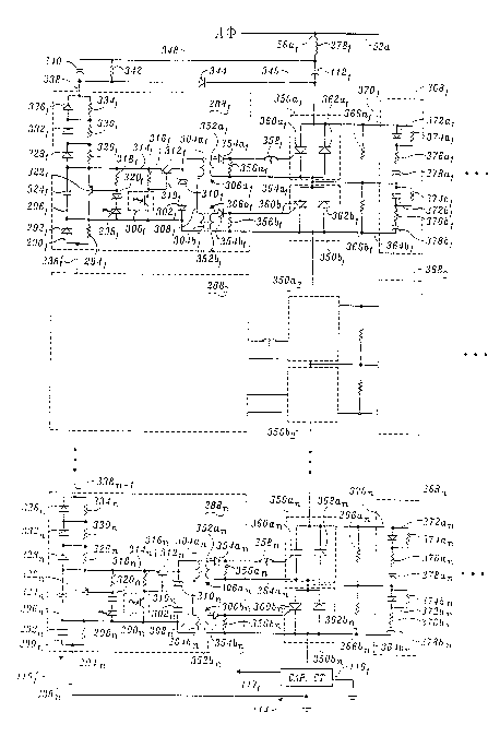
lines 52. An optically triggered switch driver 110' can instead be used for this20 purpose. One such switch driver 1101', for one compensation capacitor 1121 onA phase is shown generally at reference numeral 110' in FIGURE 14. Optically
triE~ered switch driver 1101' includes a plurality of optical trigger circuits 288
connected in series, each of which control two solid state switches 350a
and 350b. A plurality, n, of these solid state switches connected in a series string
25 can be selectively energized to connect compensation capacitor 1121 to ground,
thereby providing its compensation to line 52a. The volta~e on line 52 determines
the number of solid state switches 350 that must be used. To minimize the
differential voltage a&ross solid state switches 350 when they are turned on, they
are gated on only when the voltage on the line is at its peak negative value, such
30 that when initially gated on, substantially a zero charge current flows through the
solid state switches.
In the circuit shown in FIGURE 14, the voltsge on line 52a is nominally 5 KV
so that four pair of solid state switches 350a and 350b are required. Four optical
trigger circuits 288 are used to control the solid state switches. As in switch
35 driver 110, esch solid state switch 350a (350b) comprises an SCR 36Qa (360b)
connected in parallel with a diode 362a (362b). The four pairs of solid state
switches 350 are connected in series between capacitor 1121 and ground, and each
-L'~- 2 0 ~ ~ 5 ~ 7
pair of solid state switehes 350 is protected against excessive peak voltage by a
separate ~nubber circuit 368, as explained beJow.
A key element of optically triKgered switch driver 110' is a trigger
capacitor 340, which is connected in parallel with compensation capacitor 11Zl.
5 Inductor 278 is connected to both of these capacitors by a leacl 348. In addition, a
discharge resistor 342 is provided in parallel with trigger capacitor 340, but is
partly isolated from compensation capacitor 1121 by a diode 344, which has its
c~thode connected to compensation capacitor 1121 by a lead 346 and its anode
connected to lead 348 via resistor 342. The purpose of trigger capacitor 340 ~s
~ explained below.
Lead 338' connects each trigger circuit 288 to a lead 290, which is connected
to the anode of a diode 292 and a resis,tor 294. I)iode 292 and resistor 294 arearranged in parallel; the cathode of diode 292 is connected by a lead 296 to
several components, including an energy reservoir eapacitor 324, the collector of
an NPN transistor 322, the anode of a light errlitting diode 298, the collector of a
phototransistor 300, the cathode of a diode 302, and a primary winding 304b of apulse transformer 306. A lead 308 connects primary ~,vinding 304b with one end of
another primary winding 304a. The opposite end of primary winding 304a is
eonnected to the eathode of a zener diode 310 and to the eolleetor of an NPN
transistor 312. A lead 314 eonnects the emitter of NPN transistor 312 to a
resistor 316, the opposite side of which connects to the emitter of
phototransistor 300 and to the base of NPN transistor 312 through a lead 319. Inaddition, lead 314 eonnects to a resistor 318, the opposite end of which is
connected to the anode of a zener diode 320. The cathode of zener diode 320 is
eonnected to the cathode of LED 298 and its anode is connected to the base of
NPN transistor 322. The emitter of ~7PN transistor 322 eonnects to lead 314, so
that its emitter and collector are in parallel with energy reservoir capacitor 324.
Lead 314 conneets to a string of parallel resistors and diodes, which eonnect
to a lead 338' tor a lead 338 at the top of the string). Speeifically, a resistor 326
is eanneeted in parallel with a diode 328, a resistor 330 in parallel with 8
diode 332, and a resistor 334 in parallel with a diode 336. Diodes 328, 332,
and 336 are oriented to convey positive eharge eurrent to eharge trigger
eapaeitor 340; resistors 294, 326, 330, and 334 are relatively high-value resistors
to provide a trigger potential equalizing means arranged to balanee the voltage
distribution across the plurality of series-eonnected trigger eircuits 288 in respect
to the voltage across solid state switches 350.
2~7~ 7
-25-
Pulse transforrner 306 includes a seconclary winding 352a, which i~
inductively coupled with primary winding 304a and a secondary winding 352b
inductively coupled with primar~ winding 304b. The anode of a diode 354a is
connected to one end of secondary winding 352a; similarly, the anode of a
diode 354b is connected to secondary winding 352b. A resi~tor 356a e~tends
between the cathode oî diode 354a and a lead 364a that is connected to the otherend of secondary winding 352a. A resistor 356b is similarly connected in respectto a lead 364b and secondar~ winding 352b. A resettable circuit brcaker 358
(thermal switch) is provided betweerl the common node at the cathode of
diode 354a and resistor 356a, and the gate of SCR 360a. However, since only one
such resettable circuit breaker is required for each optical trigger circuit 2a8, the
common node at the cathode o~ diode 354b and resistor 356b is directly connectedto the gate of SCR 360b.
Each snubber circuit 368 inc~udes a diode 372a connected in parallel with a
resistor 374a. The cathode of diode :~72a and one end of resistor 374 are
connected by a lead 370 to the cathode of diode 3~2a in solid state switch 350a,and thus to solid state switch 350b in the above solid state switch (if any) in the
string. If at the top of the string of solid state switches 350, lead 3?0 connects to
reactive compensation capacitor 1121. The anode of diode 372a and the other end
of re~istor 374a are connected to a resistor 376a, which is in series with a
capacitor 378a. Similarly, a diode 372b, resistor 374b, resistor 376b, and a
capacitor 378b are provided for protection of SCR 360b and diode 362b. A
lead 364b connects capacitor 378b to SCR 360b and diode 362b in switch 350b.
Resistors 366a and 366b divide the static blocking voltage equslly across the
SCR/diode pairs (SCRs 360a/diode 362a and SCR 360b/diode 362b).
Capacitors 378a and 378b equali~e the dynamic voltage on each SCR/Diode pair,
in addition to providing snubber circuit functions. Diodes 372a and 372b limit the
discharge current from 378a and 378b to protect SCR 360a and 360b, respectively.Optically triggered switch driver 11D' operates in three states, including a
30 charging state, a holding state, and a discharge state. During the first negative
h~lf cycle of potentisl on the distribution line 52 with which it is associated, it is
in the char~ing state. In this state, current flows from ground through diodes 292,
capacitor 324, and through diodes 328, 332, and 336 in each of the optical trigger
circuits 288, to charge trigger capacitor 340 and energy reservoir
35 capacitors 3241 n. After energy reservoir capacitor 324 is char~ed to a relatively
small voltage in each optical trigger circuit, zener diode 320, NPN transistor 32~,
and resistor 318 clamp the voltage, forcing the excess current to flow through
20~7~57
-26-
transistor 322. As current flows through them, LED~ 293 emit light, indicating
thHt optically triggered switch driver 110' is in its charging stAte. A~ter energy
storage capacitors 3241 n char~e to their clamp voltage, trigger capacitor 340
continues to charge to the negatiYe pe~k voltage of line 52a minus n tim~s the
5 clamp voltage on capacitors 324, as given by the formula:
(V~n - n~vclamp)=vc34o~
where Vm - the negative peak voltage on line 52a, Vcl~mp - the maxirnum
(clamped) voltage allowed on capacitors 324.
Once trigger capacitor 340 has been charged to the negative peak voltage on
10 line 52, the charging process stops as all of the diodes that previously carried
charging current become reversed biased. At the same time that the sum of
trigger capacitor 340 and energy reservoir capacitors 3241_n charges to the
negative peak voltage on the l;ne, compensation capacitor 112 also charges to
that voltaFe. This establishes a reverse voltsge of n~Yclamp across diode 344.
15 Assuming that compensation capacitor 112 i3 not required for compensation at
this time, optically triggered switch driver 110' enters the holding state.
During the holding state, the voltage across the series connected string of
solid state switches 350 valies between zero and two tirnes the absolute
peak voltage (i.e., Voltage = VmaX(1 ~ sin(tl,t)) and the voltage across the
20 series connected string oî energy reservoir capacitors 324 also varies in
MAGNITUDE betwe~n zero and two times the absolute peak voltage, but varies
in actual value with an offset of -n~V~lamp, so that the actual voltage
value varies from -nVclamp ~ ~rmax (1+sin(~t~. It should be apparent that when
the voltage on line 52 is at the peak negative value, the voltage at the top
25 of the string of solid state switches is zero, and the ~oltage at the top of
the string of energy reservoir capacitors 324 is -n~Vclamp.
Whenever a specific compensation capacitor 112 is required to compensate
an inductive load, light pulses are supplied to each phototransistor 300 in
optically triggered switch driver 110' over optical fibers 106. This light
30 pulse signal comprises the 30 window of 5 kHz pulses. Each of the 5 kEIz pulses
in this light pulse envelope signal turns on phototransistors 300, thereby
causing NPN transistors 312 to conduct. When NPN transistors 312 begin to
conduct, the charge stored on energy reservoir c~pacitors 324 is conveyed
through primary windings 304a and 304b of each pulse transformer 3U6. These
35 5 kHz current pulses through the primary windings of the pulse transformer
~75~7
-Z7-
csuse a corresponding 5 kHz current to flow in secondnry windings 352a snd 352b,which is applied to the gat~s of SC~s 360a ancl 360b, respectively. The gate
current turns on these SCRs in each of solid state switches 350, discharging
trigger capacitor 340 through diode 344 and enabling the selected compensation
5 capacitor 112 to offset the inductive load by providing a path for positive current
flow to ground.
Zener diode 310 and diode 302 comprise a "free wheeling circuit" that
carries inductive current between each of the 5 kHz pulses in the 30 window. Asnoted above, the 30 window of 5 kHz pulses insures that harmonic distortion or
l0 transients in the voltage on line 52 cannot prematurely turn off solid state
switches 350 by causing a brief r&versal in the direction of current flow through
the SCRs. Diodes 354a and 354b block reverse ~ate current to SCRs 3fiOa
and 360b, respectively.
A current transformer 116 is disposed at the bottom of switch circuit 114 to
15 monitor the current between ground and compensation capacitor 112, thereby
providing a feedback signal that is supplied through lead 117 (as shown in
FIGURE 1). This feedback signal is used to determine whether the compensation
capacitor is properly connected to provide compensation when the light pulse
signal is supplied to trigger its functional connection to line 52. Current
20 transformer 116 thus detects a fault condition if an expected current flow tocompensation capacitor 112 (i.e., reactive power compensntion) does not occur.
From the preceding discussion, it should be apparent that the time required
by local PC controller 70 for determining the appropriate reactive power
compensation capacitance for each line 52 and for eontrolling the connection of
25 the required capacitance to the line is much less than the duration of each cycle
of the voltage waveform per phase. FIGURE 15 shows several cycles of
normalized voltage waveforms for each of the three phases. Once local PC
controller 70 determines the specific reactive power compensator capacitors thatshould be conne~ted to lines 52, during interval A, a substantial time rernains for
30 data acquisition. The time required by local PC controller 70 to determine the
required reactive power compensation is identi~ied for each phsse in this Figureby the intervals "A." The relatively longer remainin~ time identified as intervals
"B" can be used for other tasks, such as data acquisition. During intervals 13, locsl
PC controLler 70 can digitize the signals produced by the transducers in transducer
35 instrumentation bank 78 and can display the i~stantaneous or average values
indicated by those signals.
.~ 2~7~
Local PC contloller 70 does not directly control the times at which the
selected compensation cnpacitors are connected to lines 52. Its principal function
is determination of the required cornpensation and selection of the specific
compensation capacitors 112 that will provide the compensation. The remaining
5 time is spent performing data acquisition in a main program shown in
FIGURE 16A. Timing signals output from timing waveform logic circuit 86 are
operative to initiste an interrupt at any time during the data acquisition
sequence. In response, local PC controller 70 bre~ks out of the main program andis required to carry out the control funct;ons shown in FICURE 16~. FIGURE 16C
10 illustrates details of the data acquisition function performed within the main
program.
Referring initially to FIGURE 16A, the main program starts at block 377 and
begins by initializing the system at block 379. During this step, the main program
clears all variables and initializes any constants used in data conversion. The
15 main program then enters the data acquisition routine at a block 380, and
continuously loops through this routine until an interrupt signal is received from
timing waveform logic circuit 86. The interrupt signal causes the local PC
controller to perform a control interrupt in a block 381, so that it can carry out
the control functions in a block 382, discussed below in respect to FIGURE 16B.
20 After the control functions are completed in block 382, local PC controller 70
returns to the point in the data acquisition routine 380 at which it was initially
interrupted.
Detnils of data acquisition routine 380 are shown on FIGURE 16C beginning
at a start block 380a. Local YC controller 70 receives the transducer analog
25 signals in a block 380b. Th~se signals are input to an A-to-D circuit board (not
shown~ within the local PC controller and are converted to digital data in a
block 380c. The digital data are buffered for subsequent display and sveraging by
local PC controller 70 in a block 380d.
In the event that a failure flag has been set, indicating that a fault has
30 occurred with one or more of the compensation capacitors 112 (based on the
feedback signal provided from current transformers 116), a block 380e causes
local PC controller 70 to save the current instantaneous transducer data in a
block 380f and to display a failure indication in a block 380g. if the componentf~ilure flag has not been set, or subsequent to display of a failure condition, the
35 data corresponding to the signals from each of the transducers are averagPd in a
block 380h. After accumulating and averaging a predefined number of values for
each signal, an average value for each of the data signals produced by the
2067~
~9
tran~ducers is saved in a block 380j. However, decislon block 380i avoids savingthe current av~raged value for the data prior to the predefined number of valueshaving been obtsined. In a block 380k, the averaged tor instantaneous data) are
dispJayed. The program then loops back to block 380b.
The control routine performed by local PC controller 70 starts in
FICURE 16E~ at a bJock 383. In a block 384, the specific mode in which local PC
controller 70 is intended to operate is identified. Either a local operator or aremote opPrator (using remote PC controller 72 connected via communications
link 74) can effect operation of reactive power compensator 50 in one of severaldifferent modes, including: (a) a VAR control mode in which a predefined VA~
level is maintained on each line 52, (b) a power factor control mode in which a
predefined power factor is maintained on each line 52, (c) a line voltage control
rnode in which the voltsge on lines 52 is maintained as a predefined level, and (d) a
time control mode in which a predefined reactive power compensation is provided
in accordance with a time scheduie or table (that is stored in memory) indicating
the time of day at which an inductive load connected to the line should be
compensated. The operator can also select a manual mode in which specific
compensation capacitors 112 are connected to each line.
In a block 385, the multiple:ced potential signals and current transformer
signals output from sample and hold cireuit 96 (see FIGURE 1) are input to the
analog-to-digital conversion board within local PC controller 70. Digital valuescorresponding to these signals are provided and can be stored for display duringthe data acquisition routine. In a block 386~ the required compensation is
determined. This determination may be made by computing the compensation
based on the reactive current measured as the voltage on a phase crosses ~ero orcsn be determined using a look-up table. The specific compensation capacitor(s)
required for each line 52 are determined in block 386, and in a block 387, a control
signal is generated by local process controller 70 that selects the specific
compensation capacitor(s) 112 to be connected to each line 52 at the negative
peak of the potential on each of those lines. These determinations can be made as
often as twice each cycle/phase.
In a block 388, local PC controller 70 checks the feedback signals from
current transformers 116 to determine if the selected compensation capacitors
are in fact operatively connected to the lines. If a failure or fault is detected,
the failed condition is reported by setting a fail flag in a block 390.
In the event of a fault condition, local PC controller 70 can select an
alternate configuration of compensation capacitors 112. For example, assume
~75~7
-30-
that IOCRI PC controller 70 has determined that 400 KVARs of reactiYe power
compensation are required for A phase. f-Iowever, a fault flag indicates that orle
of two 200 KVAR compensation capacitors 112 previously selected has not been
successfully connected to provide this compensation to line 52a. ~ssurne also that
50 KVA~ and 100 KVAR compensation capacitors 112 are available for use on
A phase. In this case, local PC controller 70 selects the 50 KVAR and 100 KVAR
compensation capacitors 112 in place of the failed compensation capacitor,
thereby providing the best available alternative compensation (a total of
350 KVAR). Triggering determination for the alternate capacitor configuration
occurs in a block 391 in the event that the fail flag is set in block 3~0.
Thereafter, in a block 392, the triggering signals used to selectively control
specific compensation capacitors for esch line are transmitted. Alternatively, if
in block 389 a failure is not detected, the original compensation capacitor
configuration is triggered in block 392. Following the completion of this control
routine, the program returns to the data acquisition routine at the same point it
was interrupted.
Microcontroller Reactive Power Compensator
A second embodiment of the reactive power compensator is shown in
FIGURES 17A, 17B, and 17C generally at reference numeral 50'. In reactive
power compensator 50', the potential signals on each of lines 52a, 52b, and 52c are
not used to develop timing signals as in reactive power compensator 50. Instead,the timing signals are developed from an internal timer, which is synchroni~ed to
the potential on the line, as will be apparent from the following explanation.
Referring first to FIGURE 17A, a filter printed circuit board 400 is shown
that includes components for processing current and voltage signals for one
phase. A separate filter printed circuit board 400 is required for each
line 52a, 52b, and 52c, i.e., for each phase provided reactive power compensation,
but only one such board is shown. A signal indicative of the potential on one
phase, e.g., line 52a, is applied to a step-down transformer 404, which reduces the
level to approximately 12 V AC. Likewise, a signal indicative of current flowingon that phase is applied to a line current shunt resistor 406, producing a
corresponding voltage indicative of the line current. Optionally, load current can
be similarly monitored~ and a signal indicative of the load current can be supplied
to 8 load current shunt resistor 408 to develop a potential corresponding thereto.
The feedback signal from current transformer 116, which is connected to monitor
the current flowing to the compensation capacitors 112 is applied to a capacitance
current shunt resistor 41Q, likewise producing a potential indicative of that
current.
2~67~7
-31-
The signal produced by step-down transformer 404 is applied to the input of
an amplifier circuit 412, which bu~fers the signal. Likewise, each of the signals
indicative of current developed across the shunt resistors 406, 408, and 410 areapplied to amplifiers 414, 416, and 418, respectively, which amplify those signals
5 to a more usable level. The signals produced by amplifiers ~12 through 418 areconnected to th~ input of switched capacitance filters 4~2, 424, 426, and 42~.
These filters remove most of the harmonic distortion from the signals supylied by
the ampl;fiers so that generally only the fundamental 60 Hz frequency remains,
using a 6 k~lz reference signal supplied by a 6 kHz generator 420 over a lead 423.
10 The 6 kHz generator may comprise a phase-locked loop or other oscillator (notseparstely shown). The filtered signals indicative of line voltage, line current,
load current, and the filtered feedback signals (from the compensation capacitorCT) are respectively provided on leads ~48, 450, 452, and 454. In addition, the
signal output from amplifier circuit 412 is applied to a 60 Hz interrupt
15 generator 436, which produces an interrupt signal that is output on a lead 446.
After it is filtered, a signal indicative of potential output from switch
eapacitanee filter 422 is applied to the input of B 30 window circuit 434 through
a lead 430 and also supplied as an output on a lead 448. The 30 window eircuit
produces a square wa~te on a lead 44~ that is approximately 30 wide and begins at
20 about t~le point at whieh the potential signal is at its negative peak.
As shown in FIGURE 17B, reactive power compensator S0' includes a
controller 442. This ccntroller carries out all required timing functions and
processing to determine and selectively conneet the required compensation
capacitor(s~ 112 for a single phase. A generally conventional power supply 440 is
2S also included to provide various voltages used by the components of reactive
power compensator S0'. Controller 4~2 receives the interrupt signal from filter
printed circuit board 400 via lead 446, which is connected to the interrupt port of
the controller. The interrupt signal is generated each time that the potential
signal output from amplifier circuit ~12 (in FIGUR~ 17A) passes through zero in a
30 positive direction and is used to synchronize controller 442 to the voltage
waveform on the phase for which it controls reactive power compensation. That
interrupt signal is used in connection with an internal timer having a time baserefereneed to the frequency of a ~uartz crystal 466. Quartz crystal 466 and a
eapacitor J~68 are connected to crystal time base inputs of controller 442 and
3S provide a very accurate frequenc~ reference used by it to determine the time at
which the reactive power compensation should be computed and connected. For
example, based upon the interrupt signal, controller 442 samples the signal
5 7
-32-
indicative of the current on line 52 at a computed time corresponding to the zero
crossing of the potential waveform. Controller 442 determines the current based
on the signal supplied on lead 450, which is connected to one of its data ports.Controller 442 comprises a CPU, an 8-bit analog-to-digital converter, timer,
multiplexer, and includes both random access memory ~RAM) snd read only
memory (ROM). Several such devices are commercially available from different
manufacturers. Using its built-in, analc)g-to-digital converter, controller 442
digitizes the signals on leads 450, 452, and '154. By comparing the line currentwith the load current, i.e., by comparing the signals on leads 450 and 452
10 (assuming that an optional load current CT 496, as shown in FIGURE 17C, is being
used), controller 442 can detect a self-excitation condition in which the load is
producing current. This condition may arise when one or more compensation
cnpacitors 112 are connected to provide compensation if a switch (not shown) is
opened on lines 52, allowing an inductive load to start resonantly exciting the
15 line. Optionally, the signal indicative of load current determined by optional load
CT 496 can be used for determining the required reactive power compensation
instead of the signal ;ndicative of line current.
Since controller 442 also receives a signal indicative of the potential on
line 52 via lead 448, it can readily detect an over voltage resonant condition on
20 the line and in response, select a different reactive power compensation (or none)
to reduce the voltage. Control of line voltage represents one of several modes
noted above in which controller 442 operates. The mode of operation is set by the
operator using a mode switch 470, which is connected to controller 442 by a
lead 472.
A transmit receive bus 482 connects controller 442 to an optional local
PC 488 via leads 484 and 486. Data supplied by controller 442 can thus be
transmitted to and displayed on local PC 488. Selection of the mode in which
controller 442 operates can also be accomplished by control signals applied to
controller 44~ over leads 484 and 486 from the local PC. Communication of
30 control signals between local PC 488 and controller 442 is effected over
leads 490. Optionally, a remote computer 494, connected by a data link 492 to the
local PC, can supply control signals to set the mode of operation or to define the
required line voltage, power factor, or VAR level for the connected phase.
Remote computer 494 can also interrogate the local PC to determine if a fault
35 condition has occurred in respect to the reactive power compensation.
A watchdog timer circuit 474 is provided to check for an output pulse from
controller 442 at least once each ~0 milliseconds. In the event that the pulse is
-33- 2~
not supplied to watchdog tirner circuit 474 over a lead 476 within this time frame,
a reset signal is automatically supplied to controller 442 over a lead 480.
Lead 480 is also attached to a manual reset switch 478. Accordingly, an operatorcan initiate a manual reset of controller 442 by closing munual reset switch 478.
FIGURE 19 illustrates the watchdog timer circuit, which includes a
NAND gate 5~Q, that is connected to lead 476. The pulse supplied by
controller 442 over lead 476 is applied to both inputs of NAND gate 530, settingits output to a logic level 0. A capacitor 532 is connected to the output of NAND
gate 53D. When the output is at a logic level 0, the opposite side of capacitor 532
10 charges with current supplied from the 5 V DC supply through a resistor 536 and a
lead 534. The charge on capacitor 532 reverse biases a diode 538, causing the
inputs of a NAND gate 540, which are connected to the anode of diode 538, to go
to a logic level 0. As a result, the output of NAND gate 540 is set to a logic
level 1, which is transmitted th~ough a diode 542, cancelling the charge that has
15 built up on a capacitor 546. Capacitor 546 is connected to the cathode of
diode 542 by a lead 544; the other side of capacitor 546 connects to the +5 V DCsupply. A resistor 548 is also connected to the cathode of diode 542 and controls
the rate at which capacitor 546 charges, thereby controlling the logic level
applied to both inputs of a NAND gate 550. A logic level 1 that is produced when20 a pulse propagates through diode 542 to the inputs of NAND gate 550 causes a
logic level 0 to appear on its output.
The output of NAND gate 550 is connected by a lead 552 to the input of a
NAND gate 554. Assuming that a pulse was not provided by controller 442, the
output of NAND gate 550 is a logic level l, producing a logic level 1 on the output
25 of NAND gate 554. A resistor 560 conducts the output of NAND gate 554 to its
other input via a lead 556. A series-connected resistor 564 and a diode 562 are
connected in parallel with resistor 560, the anode of diode 562 being connected to
lead 556. A capacitor 558 is connected between ground and lead 556. A logic
level 1 output on NAI~aD gate 554 ;hus charges capacitor 558 through resistor 560,
30 until a logic level 1 appears on both inputs of NAND gate 554, changing its output
to a logic level 0. The logic level 0 on the output of NAND gate 554 is conveyedby a lead 566 through a resistor 568 to manual reset switch 478 and is connectedto the reset port on controller 442 through lead 4~0. After resetting
controller 442, the voltage on capacitor 558 discharges through diode 562 and
35 resistor 564, changing the level on iead 566 back to a logic level 1.
Referring back to FIGURE 17B. a plurality of leads 458 are connected to
output ports B0 through B3 on ccntroller 442 and convey control signals to a
2~6~.~57
--34-
tri~ger and logic circuit 456. In addition, the 30 window signal from the fil~er
printed circuit board i9 applied to trigger and logic circuit ~56 via lead 444. In
response to these control signals and the 30 window signal, trigger and logic
circuit 456 produces control signals which are conveyed over leads 460 and applied
5 to an optical driver and transmitter 462.
Optical driver and transmitter 462 produces light signals that are conveyed
over optical fibers 464 to selectively switch the compensation capacitors selected
as appropriate for providing the required compensation to one of lines 52. Each
optical fiber 464 conveys the light signal used to trigger solid stste switches 350
l0 to connect the selected compensation capacitor to the line.
Details of trigger and logic circuit 456 and optical driver and transmitter
circuit 462 are shown in FIGURE 18. Leads 458a, 458b, 458c, and 458d convey
control signals that are applied to one input of NOR gates 510a, 510b, 510c,
and 510d, respectively, in trigger and logic circuit 456- The other input to these
15 NOR gates is provided by lead 444, which carries the 30 window pulse signal.
However, the control signals supplied over leads 460 and the 30 window pulse
signal supplied on lead 444 are inverted. As a result, NOR gates 510 have a logic
level 1 output only if both inputs are at logic level 0, i.e., when the control signal
selects a compensation capacitor during the 30 window- The 30 window signal is20 redundant, insuring that a compensation capacitor is not triggered to connect to
line 52 other than during the 30 following the negat;ve peak voltage of the
potential waveform on that lane.
The output signals from NO~ gates 510 are supplied to the base of NPN
transistors 514a, 514b, 514c, and 514d through series resistors 512a, 512b, 512c,
25 and 512d, respectively. The emitters of NPN transistors 514 are each connected
to ground, and their collectors are each connected to resistors 51fi and light
emitting diodes 518, which are in series. In addition, the emitters of NPN
transistors 514 are also connected to resistors 520 and light emitting diodes 522,
which are also in series, but are in parallel with each pair of resistors 516 and
30 diodes 518. Light emitting diodes 518 provide a visual indication that a specific
compensation capacitor 112 has been selected, while light emitting diodes 522
transmit the light signal through optical fibers 464a, etc. required to trigger
conduction through solid state switches 350.
FIGURE 17C illustrates how optical fiber 464a is connected to an optical
35 splitter 500 that divides the light signal propagating through optical fiber 464a
into a plurality of light signals that are supplied through optical fibers 502 to
optically triggered switch driver 110'. Alternatively, switch driver 110 can be
5 ~ 7
-35-
used in reacti~e power compensator 50'. The light signals supplied through optical
fibers 502 simultaneously trigger each of the SCRs in the solid state switches to
conduct, connecting the selected cornpensation capacitor 112 so that its
compensation is provided to line 52a, as shown in FIGURE 17C. Similarly, each of5 the other compensation capacitors available are selectively controlled by optical
signals propagating over other optical fibers 464 to other optical splitters (not
shown), to compensate an inductive load ~98, which is connected to line 52a. In
sddition, each of the two other phases, lines 52b and 52c, are similarly separately
provided an appropriate reactive power compenss.tion by selectively controlling
10 the cornpensation capacitance connected to those lines.
Reactive power compensator 50' has several advantages over reactive power
compensator 50. Since each phase is controlled in respect to timing ~ignals
derived from the voltage waveforrm on that phsse, it is not necessary that al]
three phases be operational to develop timing signals, as is the case in reactive
15 power compensator 50. Furthermore, since the timing is controlled in respect to
an internal timer in controller 4~2, a substantial simplification and reduction in
the number of components required is effected. Controller 442 also benefits fromthe inelusion of watchdog timer circuit 474 to insure that it is operating
properly. Since all of the timing events are developed in software in respect to20 the internal timer, controller 442 can easily be modified by changing the program
logic used to control it. Local PC 488 is not re9uired for determining reactive
power compensation; however, it can be used for data acquisition, if desired.
The program logic implemented by controller 442 is disclosed in
FIGURES 20A and 20B. The main program logic implemented by controller 442
25 starts at a block 580. In a block 582, controller 442 initializes the system,
resetting all the variables to zero. Subsequently, in a decision block 534, the
program determines if local PC ~88 has provided a command, such as a change in
operating mode. lf so, decision block 584 branches to a block 586, which processes
that eommand. Thereafter, or if a command from local PC 488 has not been
30 received, the main program loops back to check again for a PC command. When
the manual mode is selected, the operator can use the local PC to select specific
eompensation eapacitors 112 that controller 442 connects to the line. In this
mode, the controller does not seiect or determine the required compensation likeit does in the autornatic mode. .~t any time during the processing of a command
35 from the local PC, an interrupt can be initiated in response to the interrupt signal
input on lead 446. If an interrupt occurs, the appropriate control action is taken
in a block 590; thereafter, the controller returns to the main loop at the point it
was interrupted.
2~i7~
36
In FIGURE 20B, the control logic implemented each time th~t an interrupt
signal occurs on lead ~46 is illustrated. Following a start block 592, the operating
mode of the reactive power cornpensator is checked in a mode selection
block 596. A command input from local PC 488 can effect modification of the
5 mode selection manually determined by mode switch 470 (in FIGVRE 17B). Thus,
for example, the operator can use local PC 438 to select a VAR, PF, line voltage,
or time schedule control rnode. In a block 598, the system variables comprising
voltage, line current, and the feedback signal indicative of the charge current
flowing into the reactive compensation capacitor are input to controller 442. In a
10 block 600, controller 442 carries out an an81Og-to-digital conversion, developing
corresponding digital signals, which are us,ed in a block 602 to determine the
required compensation, preferably using a look-up table in mernory. In a
block 604, controller 442 generates the triggering command that is output through
leads 458, as shown in FIGURE 17B.
E3ased upon the amplitude of the feedback signal indicative of charge current
supplied to the compensation capacitor (if previously connected to provide
compensation) over lead 454, controller 442 determines whether a failure or fault
has occurred in a decision block 606. If the feedback s;gnal fails to match an
expected reactive power compensation current, a failure is detected. If a
20 selected compensation capacitor 112, or its sssociated solid state switches 350
(shown in FIGURE 1?C~ have failed, controller 442 branches to a block 61û, whichprovides the triggering signals for a best av~ilable alternative cornpensation
capacitor configuration. If a failure has not occurred, or following selection of
the alternate configuration, the controller determines whether it is time to
25 provide the trigger signals on leads 458 in a decision block 612. As explained
above, these trigger signals are logically combined with the 3a~ window signal on
lead 444 in trigger and logic circuit 456 to control production of the light signals
that selectively activate connection of each compensation capacitor 112 to the
line). If not, controller 442 continues to loop until it determines that sufficient
~O time has elapsed since the interrupt signal occurred for the potential on theassociated phase to reach the negative peak level. At that point, in a block 614,
the controller transmits triggering signals over leads 458, which cause the
appropriate reactive power compensation capacitance to be connected to one of
the lines 52.
While the present invention has been disclosed in respect to several
preferred embodiments, those of ordinary skill in the art will appreciate that
further modifications can be made thereto consistent with the claims that follow
2 O 6 7 ~ 5 7
-37-
below. Accordingly, the scope of the invention should not in ~ny way be limited
by the description of the preferred embodiments, but instead, should be
determined entirely by reference to the claims.