Note: Descriptions are shown in the official language in which they were submitted.
200~~~2
SPECIFICATION
Title of the Invention
Superconductor magnetic shield
Background of the invention
1. Field of the Invention
The present invention relates to improvements of
a magnetic shield for shielding intense magnetic
fields, more particularly, improvements of a magnetic
shield having a large area to prevent magnetic
leakage in wide x~anges.
2. Prior art
To avoid adverse effects of magnetic fields
generated from magnets or other substances, the art
of magnetic shields which are made by using plate-
shaped or sheet-shaped superconductors refrigerated
below a critical temperature where superconductivity
is generated is known as a conventional art for
magnetically shielding a certain internal space. To
achieve the object of shielding such magnetic fields,
the second class superconductor which operates in the
mixture region of the superconducting and normal
conducting conditions is used more preferably than
the first class superconductor, since the upper
1
2U~~38N
critical temperature of the second class
superconductor is higher than that of the first class
superconductor.
The maximum magnetic field shielding intensity of
a superconductor, that is, the shielding intensity of
a superconductor having a shape of a plate, sheet,
film or membrane (in the general explanations
described below simply referred to as "layer") for
completely shielding external magnetic fields is
significantly dependent on the class, size and shape
of the superconductor. As pointed out in the patent
specifications cited below by the inventors of the
present invention, the maximum magnetic field
shielding intensity of a superconductor increases
abruptly as its thickness increases in a limited
range. If the thickness increases over a certain
value, the increasing rate of the maximum magnetic
field shielding intensity becomes gentle. This
indicates that an inflexion point is present on a
curve which represents the relationship between the
thickness of the superconductor and its maximum
magnetic field shielding intensity. Considering this
phenomenon, the inventors of the present invention
2
~d~8~~~
have proposed a magnetic shield, the maximum magnetic
field shielding intensity of which is significantly
enhanced by using superconductor layers, the
thickness of which is made smaller than that
corresponding to the reflection point of the magnetic
field shielding intensity, by laminating a
superconductor layer with a normal conductor layer
such as aluminum foil and by increasing the number of
laminated layers (Japanese Laid-open Patent Appln.
61-183979 , USP 4803452, USP 4797646, fan. PAT.
1261050, EP Appln. 86 101613. 7-2208).
To expand the range of a magnetic shielding space
by enlarging the area of a magnetic shield, the size
of a single superconductor layer is limited owing to
the limitation in the production requirements of
superconductors. In the case of producing larger
superconductor layers exceeding the limitation, an
art for enlarging such a magnetic shield by mutually
overlapping the end sections of a plurality of oxide
superconductor ceramic plates for example and by
sticking the end sections together with conductive
adhesive is known~(Japanese Laid-open Patent Appln.
63-313897). The inventors of the present invention
3
20~~~~
have also proposed a magnetic shield made by sticking
a plurality of small superconductor pieces onto the
external or internal surface of a cylinder with its
one end closed (Japanese Laid-open Patent Appln. 1-
302799).
These days, superconductor magnets are made
larger to generate more intense magnetic fields.
Because of this enlargement, the space ranges
affected by the intense magnetic fields axe also
expanded. To shield unnecessary permeation of
intense magnetic fields, magnetic shields which can
securely shield intense magnetic fields over large
areas have been requested. Such magnetic shields are
applied to superconductor motors and superconductor
generators, as well as superconductor magnets
themselves used in linear motor cars and
electromagnetic propellent ships.
The maximum magnetic field shielding intensity of
a plate-shaped magnetic shield for completely
shielding a magnetic field is apt to become lower at
the external peripheral section than at the central
section of the magnetic shield. In the case of a
disc-shaped magnetic shield for example, the maximum
4
magnetic field shielding intensity is lower at its
peripheral section farther away fram its central
section in the radial direction. For this reason,
although complete shielding is possible at the
central section, a part of magnetism permeates the
external peripheral section, causing magnetic
leakage. Consequently, to completely shield a
constant external magnetic field permeating a surface
area, shielding is necessary at the central section
of the surface area of the magnetic shielding plate
by using a magnetic shield having the maximum
magnetic shielding amount exceeding the external
magnetic field intensity generated at the end of the
surface area. As a result, the size of the magnetic
shield must be considerably larger than the surface
area.
A serious problem in the magnetic shielding
process is the generation of a flux jump phenomenon
wherein magnetic flux permeating the external
peripheral section of the magnetic shield flows
abruptly to the central section of the magnetic
shield. If this occurs, the magnetic shield is
heated locally and its superconducting condition is
~O~~~J~
converted into a normal conducting condition, thereby
causing magnetic field leakage aver the entire
magnetic shield. If this flux jump occurs once, the
magnetic shield cannot act as a superconductor and
completely loses its magnetic shielding function.
Since the amount of generated heat is greater as the
transfer distance of magnetic flux is larger, it is
difficult to stably maintain the superconducting
condition in an intense magnetic field.
In the magnetic shield of the above-mentioned
prior art, which is made large by mutually laminating
and sticking a plurality of superconductor ceramic
plates, superconductive shielding current flows
across every two ceramic plates. The structure of
the magnetic shield is thus considered to be the same
as that comprising a single superconductor, thereby
being apt to cause the danger of losing the magnetic
shielding effect due to the generation of the flux
jump.
In the case of a tubular magnetic shield formed
by pressing and sticking superconductor pieces
(comprising superconductive low-melting-point alloy
powder) onto the surface of a tube, the structure of
6
20~8~~~
this magnetic shield is the same as that of a tube
formed to have a large surface area made by using a
single superconductor, since the adjacent
superconductor pieces are joined by the
superconductor alloy. Accordingly, the maximum
magnetic shielding amount of the magnetic shield is
lower at the upper peripheral section of the opening
area of the tube and lowest at the sealed end section
of the bottom of the tube, causing the danger of
losing the magnetic shielding effect due to the
generation of the flux jump at such sections.
As a countermeasure for reducing the effect of
the flux jump, a plurality of small through holes are
provided in the surface area of a thin superconductor
film such that the transfer range of the magnetic
flux is limited to reduce heating and prevent a chain
reaction of magnetic flux flow (Japanese Laid-open
Patent Apple. 63-233577, USP 4828931, Can. Pat.
1296089, UK Pat. 2203909, German Pat. Apple. P38-
09452. 5-34, FR 8803822). Even when a magnetic
shield is enlarged, however, it still has a problem
of reduction in the maximum magnetic field shielding
intensity at its peripheral section.
7
Summary of the invention
It is therefore the first object of the present
invention to provide a magnetic shield capable of
compensating for the reduction of the maximum
magnetic shielding amount at the peripheral section
of the magnetic shield and also capable of
effectively shielding the intense magnetic field at a
large surface area of the magnetic shield, and to
prevent superconductivity from being lost owing to
the generation of the flux jump which is relevant to
the enlargement of the magnetic shield, thereby
ensuring stability during magnetic shielding.
The second object of the present invention is to
provide a superconductor magnetic shield capable of
achieving completely zero magnetic field intensity
even in the presence of a locally intense magnetic
field so that the magnetic shield can cope with the
spatial change in the magnetic field intensity in an
ununiformed magnetic field.
To accomplish these objects, the superconductor
magnetic shield of the present invention is made by
arranging and sticking a plurality of small
superconductor layers (each of which is hereafter
8
20~~~8~.
referred to as "unit layer") OIlto the surface of a
substrate (support member) having a desired shape,
and the peripheral section of each unit layer is
overlapped with the peripheral section of another
unit layer in the normal direction in order to
uniformize the maximum magnetic field shielding
intensity of the magnetic field over the entire
substrate or to locally strengthen the shielding
intensity as a general feature.
Brief Description of the Drawings
Fig. 1 (A) shows a general radial direction
distribution of the maximum magnetic field shielding
intensity of a disc-shaped superconductor unit layer.
Fig. 1 (B) shows the relationship between external
magnetic field intensity and the magnetic shielding
amount of the superconductor unit layer.
Fig. 2 is a sectional view of a magnetic shield
formed by overlapping the peripheral sections of
rectangular thin superconductor unit layers of an
example of the present invention and also shows a
distribution of the maximum magnetic field shielding
intQnsity at the illustrated cross-section.
Fig. 3 is a plan view of a magnetic shield made
9
rJ
by sticking square superconductor unit layers. Fig.
4 (A) and Fig. 4 (B) are respectively a plan view and
a vertical sectional view of a magnetic shield made
by sticking disc-shaped superconductor unit layers.
Fig. 5 (A) is a plan view of a magnetic shield
provided with abutted and stuck square sheet-shaped
superconductor unit layers, and Fig. 5 (B) and Fig. 5
(C) are respectively a plan view and a vertical
sectional view of a magnetic shield with two
vertically arranged layers comprising the sheet-
shaped superconductor unit layers of the example of
the present invention.
Fig. 6 (A) is an arrangement view of abutted and
stuck disc-shaped superconductor unit layers and Fig.
6 (B) 3.s an arrangement view of three vertically
laminated layers of the disc-shaped superconductor
unit layers of the example of the present invention.
Fig. 7 is a vertical sectional view of a
container-shaped magnetic shield, the internal
surface of which is covered with a plurality of
layers comprising the sheet-shaped superconductor
unit layers of the present invention. Fig. 8 is an
outline sectional view of an apparatus for testing
10
20G~~~
the magnetic characteristics of the magnetic shield
shown in Fig. 7.
Detailed Description of the Invention
The superconductor magnetic shield of the genus
invention of the present invention comprises a
substrate and a plurality of independent
superconductor unit layers arranged adjacent to one
another and stuck onto the surface of the substrate,
wherein the peripheral section of each unit layer is
overlapped with the peripheral section or the central
section of another adjacent unit layer in a non-
direct contact manner in the normal direction of the
substrate so that the magnetic shielding intensity at
these overlapping sections can be increased
substantially.
This genus invention can be generally classified
into a first invention and a second invention.
In the case of the superconductor magnetic shield
of the first invention, the surface areal plane
including the superconductor unit layers of the
above-mentioned structure is a single layer in the
normal direction and the above-mentioned peripheral
sections are overlapped mutually within the single
11
layer. This first invention corresponds to claim 2.
In the case of the superconductor magnetic shield
of the second invention, the surface areal planes
including the superconductor unit layers of the
above-mentioned structure are laminated to form a
plurality of layers in a non-direct contact manner in
the above-mentioned normal direction, the peripheral
sections of the unit layers are in abutting contact
with or proximate to the peripheral sections of the
adjacent unit layers within the single layer, and the
above-mentioned peripheral sections of the unit
layers are overlapped mutually between every two
layers in the normal direction. This second
invention corresponds to claim ~.
The first invention further includes a
superconductor magnetic shield wherein a plurality of
layers, each comprising a plurality of superconductor
unit layers, are laminated (claim 3), and in the same
way, the second invention includes a superconductor
magnetic shield wherein three or more layers are
laminated (claim 6) and used to cover the surface of
the substrate.
In addition, the present invention also includes
12
~~~83~~
a superconductor magnetic shield wherein the number
of the layers comprising superconductor unit layers
is increased at the magnetic flux concentration
sections of the magnet shield (claim 7).
First, the technical matters common to the first
and second inventions are described below.
The substrate is formed in accordance with the
desired shape of the superconductor magnetic shield
and is determined considering the shape of the
superconductor magnet to be covered and the space
range to be shielded. The substrate is mainly made
of non-magnetic normal conductor material, such as
copper, aluminum, stainless steel or low-temperature
synthetic resin and is formed into a shape of a flat
plate, curved plate or container.
The superconductor unit layer includes films or
plates made of superconductor material. Although it
can be a single thin superconductor plate, it
preferably comprises laminations of thin
superconductor plates and thin non-magnetic metal
plates.
As superconductor material, Nb-Ti alloy, mixed
crystal of NbN and TiN, Nb3Al, Nb3Ge, Nb3 (A1, Ge),
1~
Nb3Sn, Y-Ba-Cu-0-based oxide, Bi-Sr-Pb-Ca-Cu-0-based
oxide or T1-Sr-Ca-Cu-0-based oxide are used.
The superconductor unit layer can have a simple
shape of a square, hexagon or circle. The
appropriate size of the unit layer is 5 to 100 cm in
diameter in the case of a circle.
The unit layers are stuck together with low-
temperature organic adhesive or normal conductor
low-melting-point alloy onto the surface of the
above-mentioned substrate. When sticking unit layers
to provide only one layer, the peripheral sections of
the unit layers are overlapped mutually to prevent
formation of any gap which is not covered with unit
layers as viewed in the normal direction to the
surface of the substrate and to completely cover the
substrate. In this case, it is important that the
overlap is performed so that the peripheral section
of each unit layer does not make contact with those
of other adjacent unit layers. To accomplish this,
the adhesion layer formed by the above-mentioned
adhesive should be insulated, or organic insulation
films should be intervened at the overlapping
sections or the front arid rear surfaces of the
14
20~~~p .
superconductor unit layers should be a lamination
covered with normal conductor metal, such as copper
film or aluminum film.
To form two or more layers comprising the
superconductor unit-layers and to stick the layers
onto the above-mentioned substrate, the unit layers
are stuck sequentially onto the lower superconductor
unit layer with the above-mentioned adhesive or
normal conductor low-melting-point alloy. At the
time of this process, although the thin
superconductor films of the same layer can be abutted
and arranged such that a gap generates between the
films, the superconductor unit layers of the second
layer must be arranged in the normal direction such
that they cover the gaps generated in the first
layer.
In addition, an electric insulation layer or a
normal conductor layer should be intervened in the
same manner as described above such that the
superconductor unit layers of the first and second
layers do not make contact with each other.
Generally, a superconductor sheet, for example, a
disc-shaped superconductor does not have uniform
15
20G8~~
magnetic shielding capability over its entire
surface. The maximum magnetic field shielding
intensity Hm of the superconductor at the time of
complete shielding of an external magnetic field is
highest at the center of the disc. The intensity
lowers at the external peripheral section and becomes
zero at the end section of the disc. The maximum
magnetic field shielding intensity of the disc-shaped
superconductor is shown as a skirt-shaped curve as
shown in Fig. 1 (A) when a radius is taken as a
variable. Fig. 1 (B) shows the relationship between
an external magnetic field intensity and a magnetic
shielding amount off (a difference between the
magnetic field intensity obtained when a magnetic
shield is present at a measurement position and that
obtained when the magnetic shield is absent) measured
in the radial direction from the central section c to
the end section a of the disc-shaped superconductor.
According to the figure, the magnetic shielding
amount at the central section c is equal to the
external magnetic field intensity in response to the
initial increase of the external magnetic field
intensity and the magnetic field does not permeate
16
zu~a~~z
the superconductor. However, if the external
magnetic field intensity becomes greater than the
maximum magnetic shielding amount oHm, the magnetic
shielding amount off becomes smaller instead. In
other words, if the external magnetic field intensity
is greater than the maximum magnetic shielding amount
~Hm, the magnetic flux of the magnetic field becomes
to penetrate the superconductor. When the maximum
magnetic shielding amount oHm is assumed to be the
maximum magnetic field shielding intensity Hm, the
value of Hm becomes smaller at positions farther away
from the central section of the disc and becomes zero
at the end section, resulting in no magnetic
shielding capability.
The maximum magnetic field shielding intensity Hm
at the central surface section of a sheet-shaped
superconductor differs depending on the type,
structure and thickness of the superconductor. When
a disc-shaped superconductor is taken as an example,
the intensity Hm generally increases abruptly as the
disc diameter increases up to about 50 cm. The value
still increases gradually as the diameter increases
further. For this reason, the superconductor unit
17
layer is limited to a small size of 5 to 100 cm in
diameter.
The magnetic shield of the first invention is
made by arranging and sticking such small
superconductor unit layers onto the surface of the
substrate while vertically overlapping the external
peripheral sections of the superconductor unit layers
and while using care so that the adjacent
superconductors do not make contact with one another.
With this structure, the maximum magnetic field
shielding intensity at the overlapping sections is a
sum of the magnetic field shielding intensity of the
upper superconductor unit layer and that of the lower
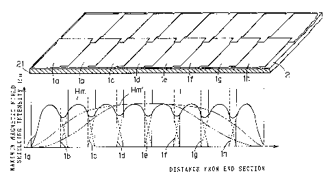
superconductor unit layer as shown in Fig. 2. By
relatively expanding the width of the overlapping
sections, the maximum magnetic field shielding
intensity values at all surface area positions of the
magnetic shield are uniformized to a value greater
than a certain value. For this reason, when a
large-area magnetic shield is formed by a single
superconductor or by laminating a plurality of small
superconductor pieces such that they make contact
with one another, the maximum magnetic field
18
shielding intensity of the magnetic shield reduces in
the wide range of the peripheral sections of the
superconductor as shown by the Hm' curve in Fig. 2.
As a result, the external magnetic field which must
be shielded cannot be shielded completely and
magnetic field leakage occurs. To solve this
problem, a magnetic shield with a surface area far
wider than the surface area o.f the external magnetic
field to be shielded is required. However, the
magnetic shield of the present invention has superior
magnetic shielding capability even at its peripheral
sections except the very narrow ranges close to its
end sections as high as the capability obtained at
its central section, as indicated by the Hm curve
shown in Fig. 2. The size of the surface area of
the magnetic shield can thus be made approximately
equal to that of the external magnetic field to be
shielded.
In the first invention, when the layer formed on
the substrate by overlapping the peripheral sections
of the superconductor unit layers is further
laminated with another layer to form two layers,
while the upper and lower superconductor unit layers
19
2~6~3~
are maintained in a non-contact manner and while the
overlapping section of each lower unit layer is
positioned at the central section of the
corresponding upper unit layer, the distribution of
the maximum magnetic Field shielding intensity of the
magnetic shield is further uniformized and flattened.
To further flatten the distribution, three or more
layers should be used.
In the second invention, superconductor unit
layers are laminated in two or more layers on the
substrate. Adjacent layers are proximate to or
abutted against each other. The peripheral section
of each superconductor unit layer of the first layer
is overlapped with one of the superconductor unit
layers of the second layer. As a result, the maximum
magnetic field shielding intensity of the
superconductor unit layer located just above the
peripheral section of another superconductor unit
layer is added to the low maximum magnetic field
shielding intensity of the peripheral section,
thereby obtaining the maximum magnetic field
shielding intensity that is larger than a certain
level over the entire surface of the magnetic shield.
20
2UU338~
In tho magnetic shield of the second invention,
there is no magnetic shielding capability at the
abutted sections between the adjacent unit layers or
the void portions proximate to the adjacent unit
layers when only the first layer comprising
superconductor unit layers is used. By laminating
the second layer comprising the superconductor unit
layers over the first layer, the magnetic field
shielding capability at the above-mentioned abutted
sections or the proximate void portions of the first
and second layers can be compensated for.
Since the magnetic shield of the present
invention is formed by sticking a plurality of
superconductor unit layers onto the surface of the
substrate while maintaining the non-contact manner in
the normal direction, the shielding current for
preventing the intrusion of external magnetic fields
flows only inside the corresponding unit layer, but
the unit layer is isolated from other adjacent unit
layers. With this structure, even if flux jump (the
abrupt transfer of magnetic flux permeated at 2,nd
transferred from the peripheral section to the
central section of the unit layer) occurs, the mutual
21
~(~~~~~'y
action between the magnetic flux and the shielding
current is limited within the corresponding unit
layer and the chain reaction of the flux jump is also
limited within the corresponding unit layer, thereby
causing no adverse effect to other adjacent
superconductor unit layers. Since the size of the
unit layer can be made small, the transfer distance
of the magnetic flux can also be made small. Even
when magnetic flux flow occurs frequently, the
heating value of the unit layer is limited. Even if
the temperature of the unit layer increases, the unit
layer can be refrigerated by immersed refrigerant
such as liquid helium. This minimizes the
possibility of raising the temperature of the unit
layer over its critical temperature, the possibility
of converting the unit layer into a normal conductor
and the possibility of losing the magnetic shielding
function of the unit layer. For this reason, the
present invention can form a large-area magnetic
shield which rarely causes unstable conditions due to
flux jump.
In particular, when the superconductor unit layer
is laminated with a normal conductor metal layer, the
22
~IIG~'~~~;~~
normal conductor metal layer shuts off the flow of
the above-mentioned shielding current of the unit
layer and isolates each superconductor layer. When
aluminum, particularly copper or silver is used as
metal, the superior heat conductivity of such metal
is significantly effective in externally dispersing
the heat generated by the flow of magnetic flux and
thus also effective in refrigerating the layers,
thereby effectively preventing instability due to the
flow of the magnetic flux.
When a single layer of the superconductor unit
layer is used, it usually comprises rolled Nb-Ti
alloy foil with a thickness of 100 ~m or less. As
the thickness is larger, the maximum magnetic field
shielding intensity of the superconductor layer
becomes greater. However, if the thickness increases
to 20 Ym or more, the increasing rate of the maximum
magnetic field shielding intensity reduces. This
increasing. of the thickness.is thus not advantageous.
Rather than using the thicker foil, a lamination
comprising Nb-Ti alloy foil of 20 ~.am or less in
thickness and normal conductor foil such as copper or
aluminum foil should be used. -Increasing the number
23
2~~~~~~
of laminations is advantageous, since the maximum
magnetic shielding amount can be made larger. When
forming the lamination comprising the Nb-Ti alloy
foil and the normal conductor foil, the sputtering
method for the Nb-Ti alloy and copper or aluminum can
be used, The sputtering method is also used when the
unit layer is formed from the mixed crystal of NbN
and TiN. More specifically, the above-mentioned
sputtering method is conducted on one or two kinds of
metal layers selected from the group consisting of
copper, aluminum, nickel, stainless steel, titanium,
niobium and niobium-titanium alloy to form the
lamination. When forming the superconductor unit
layer from Nb3Al, Nb3Ge, Nb3 (A1, Ge) and Nb3Sn, the
thin films formed by the sputtering method or the
like can be used. In addition, the films which are
heat-treated after rolling and lamination can be
used. As the normal conductor layer, one or two
kinds of metal layers selected from the group
consisting of copper, aluminum, nickel, stainless
steel and titanium can be used.
For the magnetic shield of the present invention,
a plate-shaped superconductor can be used as one of
24
' the superconductor unit layers. As the plate-shaped
superconductor, a plate made of the X-Ba-Cu-0-based
oxide, Bi-Sr-Pb-Ca-Cu-0-based oxide or
Tl-Sr-Ca-Cu-0-based oxide can be used. In addition,
a sintered plate of 0.5 to 10 mm in thickness can
also be used as the plate-shaped superconductor.
When a plurality of small through holes are
provided in the superconductor unit layer, the
transfer of the magnetic flux at the peripheral
section of the unit layer is limited in the range of
the adjacent small holes and no flux jump occurs at
the central section of the unit layer. The range of
the flux jump can thus be restricted within the range
approximate to the space between the holes, thereby
eliminating the danger of making the superconductor
unstable. If the diameter of the holes is made
larger, however, the magnetic shielding amount is
lowered. The opening area of the holes should
therefore be 3 cm2 or less and preferably the
diameter of the hole should be about 50 Vim.
'. Since the present invention provides a large-area
magnetic shield by sticking a plurality of small
superconductor unit layers onto the substrate, the
r.;d
superconductor unit layer can have a small size of
about 5 to 100 cm. Such superconductor unit layers
can thus be produced very easily. Furthermore,
magnetic shields of larger sizes or with various
curvatures can also be produced easily by sticking a
plurality of unit layers onto the substrates made by
welding and assembling.
Moreover, since the magnetic characteristics of
the unit layer can be measured accurately and easily
by ordinary test methods, the characteristics of an
assembled magnetic shield can be estimated fairly
accurately by determining the sticking method
according to the magnetic data of the unit layer.
Examples
An example of the first invention is first
explained below referring to the drawings, Fig. 3
shows an example of a magnetic shield wherein square
superconductor sheets la, 1b, ... are laminated as
unit layers on a rectangular flat substrate 2 so that
the peripheral section of one sheet is overlapped
with and stuck onto that of another sheet. As the
superconductor sheets la, 1b, ... , thin flexible
alloy plates are appropriate, and particularly a
26
20~8~~~
single layer of Nb-Ti alloy foil of 100 Ym or less in
thickness or an alternate lamination of Nb-Ti alloy
foil and aluminum foil of 20 ym or less in thickness
can be used. Low-temperature organic adhesive (not
shown) is used for sticking. An adhesive layer is
intervened between the overlapping sections of the
superconductor sheets la and 1b such that the
overlapping sections thereof do not make direct
contact with each other. When using the lamination
comprising the Nb-Ti alloy foil and aluminum foil,
the front and rear surfaces of the lamination are
covered with aluminum foil to prevent direct contact
between the overlapping sections of the adjacent
pieces of superconductor Nb-Ti alloy foil. This
method is advantageous since the adhesive for
preventing the direct contact is unnecessary.
Fig. 4 shows an example of laminating and
sticking disc-shaped superconductor sheets as
superconductor unit layers. For the superconductor
sheets shown in Figs. 3 and 4, non-flexible thin
oxide superconductor plates can also be used. Even
in this case, an organic adhesive layer is intervened
between the overlapping sections of the plates so
27
~os~~~
that the superconductors do not make direct contact
with each other at the overlapping sections, and the
superconductor sheets are stuck onto the substrate 2.
The substrate 2 of the magnetic shield shown in
Figs. 3 and 4 has a rectangular shape. By combining
a plurality of such rectangular substrates, a
container-shaped magnetic shield can be formed.
Besides, since flexible superconductor sheets can be
easily stuck onto a curved substrate, magnetic
shields having desired shapes and large areas can be
formed.
By sticking and covering one or two more layers
comprising superconductor unit layers of the same
size over the layer comprising superconductor unit
layers stuck as shown in Figs. 3 and 4, the maximum
magnetic field shielding intensity of the magnetic
shield thus obtained can be enhanced and flattened.
Examples of the second invention are then
described below.
Fig. 5 (A) shows an example wherein square
superconductor sheets used ~as unit layers are stuck
with the end sections thereof abutted. This example
is applied particularly to non-flexible rigid
28
20683~~
superconductor plates, for example the above-
mentioned oxide superconductor plates. In this ease,
a small gap is provided at each end of the abutted
section thereof to prevent the adjacent
superconductors from making contact with one another
and to allow an adhesive layer to intervene in the
gap. In the case of this method of sticking the unit
layers by abutting them, the maximum magnetic field
shielding intensity at the abutting sections is
approximately zero and magnetic leakage occurs. To
solve this problem, the abutted and stuck
superconductor plates must be laminated in two layers
as shown in Fig. 5 (B) and 5 (C), and the abutting
sections of the upper layer must be shifted in the
surface direction so that the abutting sections of
the upper layer do not coincide with those of the
lower layer. To completely prevent magnetic
shielding leakage and to uniformize the maximum
magnetic field shielding intensity, the lamination
structure should have three or more layers.
Fig. 6 (A) shows the arrangement of the first
layer wherein discs la, 1b,.... are abutted and stuck
as unit layers. In this case, even when the discs
29
20~838~
are placed in the highest density, a substantial void
portion 24 is formed among every three adjacent
discs.
As shown in Fig. 6 (H), the superconductor discs
r
1'a, 1'b, ... of the second layer are stuck and
arranged to cover the void portion 24 enclosed by
every three adjacent discs of the above-mentioned
first layer. Even in this two-layer structure,
magnetic leakage still occurs at each position where
the void portion 24 of the lower layer coincides with
the void portion 24 of the upper layer. To prevent
this leakage, the superconductor discs 1°'a, 1"b, ...
of the third layer are stuck to cover the void
portions 24 located at such coincidence positions.
By providing a lamination structure of three or more
layers, the maximum magnetic field shielding
intensity of this example can be uniformized and
flattened. The method of sticking such discs is
suited particularly for fragile~superconductor
ceramics, since disc-shaped sintered products can be
made easily.
Fig. 7 shows a vertical sectional view of an
upper part of a container-shaped magnetic shield
30
zaas3s2
wherein ~~ plurality of layers comprising plate-shaped
supercon~9uctor ceramic layers used as unit layers are
stuck inside. The three layers 11, 12 and 13
comprising the ceramic plates are stuck onto the .
inside surface of the container-shaped copper
substrates 2. Furthermore, two layers 14 and 15 are
additionally stuck onto the corner sections of the
substrate to shield the high magnetic field intensity
generated by the concentration of the magnetic lines
of force at the corner sections.
Next, the production method and test results of
the magnetic shields of the present invention are
described below.
Superconductor unit layers were produced as
follows. A lamination plate having a total of 25
layers was produced wherein each layer was made by
laminating Nb-Ti alloy and copper which were
alternately evaporated in a thickness of 0.4 ~Zm on a
copper plate measuring a thickness of 18 ym and a
diameter of 30 mm by using a sputtering apparatus.
The plate was then cut into square pieces having a
side length of 50 mm to obtain superconductor sheets.
The substrate was made of 5 mm thick copper
31
2oss~s
plate. It was formed into a pan shape having a
diameter of 400 mm and equipped with a flat bottom
and curved external peripheral sections. Over the
entire internal surface of the substrate, the 10 mm
wide overlapping sections of the above-mentioned
superconductor sheets were provided by the
overlapping method described in the explanation of
the example of the first invention shown in Fig. 3
and stuck with low-temperature epoxy adhesive to form
a magnetic shield. Two superconductor sheet layers
were provided at the central flat section of the
magnetic shield and five layers were used at the
curved peripheral sections and end sections thereof.
As shown in Fig. F3, a superconductor coil 5 was
provided at a lower section of an adiabatic vacuum
container 4 having an internal diameter of 500 mm.
Over the coil, a pan-shaped magnetic shield 3 was
disposed with its internal surface side facing
downwards. The interior of the adiabatic container
was filled with liquid helium to refrigerate the
superconductor coil 5 and the magnetic shield 3. The
magnetic field inside the container was measured at
four positions a, b, c and d over the magnetic shield
32
2~6~38~
3 by using a magnetic field measurement sensor.
The exciting current of the superconductor coil
magnet 5 was first obtained so that the measured
magnetic field intensity was 1000 G at the
measurement points a and f without installing the
magnetic shield 3. The magnetic shield 3 was then
installed at the specified position, the same
existing current was flowed in the superconductor
coil 5, and the magnetic field intensity was
measured. The measured.magnetic field intensity
values were 5 G or less at all measurement positions
a, b, c and d.
A magnetic shield made of an oxide represented by
a chemical formula of Yl.OBa2.OCu3.007-x used as an
oxide superconductor was then tested. A mixture of
Y203, BaC03 and Cu0 was heated, melted and abruptly
refrigerated, then pulverized. The power obtained in
this way was press-molded into a shape of a disc and
fired to produce a plate-shaped superconductor. To
form thin films from the oxide, the oxide powder was
applied to or printed on a metal plate made of copper
for example, then fired.
The fared superconductor discs measuring 50 mm in
33
~U6838'
diamete~:~ and 5 mm in thickness were arranged in three
layers as shown in Fig. 6 and stuck onto the internal
surface of the pan-shaped substrate made of copper
and measuring a thickness of 5 mm and an outer
diameter of 400 mm as shown in Fig. 8. The magnetic
shielding amount of this example was then measured
using the above-mentioned testing apparatus. The
maximum .magnetic shielding amount of the example was
20000 G in the 70% surface area including the central
section of the pan-shaped substrate.
Consequently, the magnetic shield of the present
invention can provide the following advantages.
Since a plurality of small superconductor unit
layers can be stuck onto a substrate while being
overlapped at their peripheral sections without
allowing the superconductors to make contact with one
another and a large-area magnetic shield can be
formed, i;he maximum magnetic field shielding
intensity of the magnetic shield can be uniformized
in the surface area of the magnetic shield without
causing t;he reduction of the intensity at the
external peripheral sections thereof except the
ranges very close to the end sections. Besides, the
34
20$382
reduction of the maximum magnetic field shielding
intensity which occurs at the external peripheral
sections of a large-area magnetic shield formed by a
continuous superconductor can be compensated for and
prevented by the magnetic shield of the present
invention. The size of the magnetic shield can thus
be made almost as large as the range of an external
magnetic field to be shielded. The magnetic shield
of the present invention can therefore be made
relatively smaller than the magnetic shield formed by
such a continuous superconductor.
In addition, since two or more layers comprising
stuck superconductor unit layers are used, the
maximum magnetic field shielding intensity of the
magnetic shield of the present invention can be
enhanced., uniformized and flattened in the external
peripheral direction.
Furthermore, when a plurality of superconductor
unit layers are abutted and stuck at their end
sections and laminated to form two or more,
particularly three or more layers, the magnetic
leakage at the abutting sections can be prevented and
the maximum magnetic field shielding intensity of the
35
2068382
magnetic shield can be enhanced significantly.
In particular, since the number of the
laminations can be increased at the end sections of
the magnetic shield, particularly in the limited
ranges exposed to high magnetic field intensity, the
magnetic shield of the present invention can cope
with the change in the intensity of local external
magnetic fields by compensation, thereby easily
achieving complete magnetic shielding.
Morecwer, since the superconductors of adjacent
superconductor unit layers are isolated so that they
do not make contact with one another, the possibility
of causing flux jump is eliminated over the entire
magnetic shield. Even if flux jump occurs, it is
limited in the range of a small superconductor and
heat generation is minimal, thereby extremely
reducing the danger of causing the superconductor to
be converted into a normal conductor. In particular,
when the superconductor unit layers have a lamination
structure comprising superconductor and normal
conductor films or when a plurality of small through
holes are provided in the superconductor unit layers,
the factors for causing instability due to flux jump
36
206838
can be eliminated substantially and the reliability
of the magnetic shield of the present invention can
be enhanced significantly.
When the magnetic characteristics, size and shape
as well .as the sticking method and the number of
laminations of the superconductor unit layers have
been knoRan, the magnetic shielding capability of a
large-area magnetic shield made by sticking the unit
layers can be estimated fairly accurately. In the
case of ~i conventional magnetic shield, preliminary
experimental testing of the shielding capability of a
practically large magnetic shield is virtually
impossible partly because larger testing apparatuses
must be used. In the case of the magnetic shield of
the present invention, it is possible to estimate the
magnetic characteristics of the magnetic shield
according to partial test results, since the unstable
phenomena due to the above-mentioned flux jump do not
occur.
3~
a