Note: Descriptions are shown in the official language in which they were submitted.
2 0 6~3
DIGITAL SIGNAL TRANSMISSION SYSTEM
HAVING MONITOR E~UIPM~NT
BACKGROUND OF THE INVENTION
1. Field of the Invention
The present invention relates to a digital
signal transmission system having monitor equipment.
The recent rapid progress in the field of a
communication technique greatly relies upon a digital
transmission system that operates to transmit digital
signals, such as telephone signals, a variety of data
signals and so on, under a time division multiplex mode.
Therefore, there is a strong demand for a reliable
monitor of a related digital signal transmission system.
That i5, it is necessary to determine if fault occurs in
the digital signal transmission system, the location of
the fault therein and further to restore the related
faulty portion quickly and correctly.
The present invention therefore provides a
digital signal transmission system having monitor
equipment that can easily achieve the monitor.
As will be explained later, the digital signal
transmission system is comprised of, as major parts, a
serial/parallel converter and a parallel/serial
converter, which play an important role when the digital
signal transmission system is incorporated into a so-
called highway transmission line, to increase the
transmission efficiency of the signals, i.e., an increase
in the transmission speed and provision of an economical
facility, and thus the converters are essential for a
highway transmission line. This being so, it is very
effective to monitor these converters per se to improve
the maintenance of the highway transmission line and also
reliability thereof.
2. Description of the Related Art
Conventionally, the digital signal transmission
2 - 2~69284
system is monitored by the use of a well known parity
check and a pass pattern check, which will be explained
hereinafter.
However, in the conventional digital signal
transmission system having monitor equipment there are
the following problems.
(1) it is difficult for the monitor equipment
to achieve a monitor of the aforesaid serial/parallel
(S/P) and parallel/serial ~P/S) converters per se, and
(2) much hardware is required for constructing
the monitor equipmen~ in the digital signal transmission
system. In actuality, there has been no practical
monitor equipment that can monitor the inside of each of
said S/P and P/S converters.
SUMMARY OF THE INVENTION
Therefore, the present invention, in view of the
above problems, strives to provide monitor equipment
incorporated in a digital signal transmission system that
is simple in construction, and is capable of monitoring
the S/P and P/S converters per se, i.e., internal
circuits of the S/P and P/S converters.
To attain the above object, the monitor equipment of
the present invention is basically comprised of:
a first means for receiving parallel pass
pattern signals passing through a S/P converter and
applying the same, after conversion into a serial pass
pattern signal, to respective channel lines for achieving
respective pass pattern checks, and
a second means for receiving each serial pass
pattern signal sent parallel from respective channel
lines and applying the same, after conversion into serial
pass pattern signals occurring at every frame
sequentially/ to a multiplexed channel line for achieving
a pass pattern check of each channel.
BRIEF DESCRIPTION OF THE DRAWINGS
The above object and features of the present
invention will be more apparent from the following
206~2~
description of the preferred embodiments with reference
to the accompanying drawings, wherein:
Fig. 1 is a block diagram of a typical and
conventional digital signal transmission system having
monitor equipment;
Fig. 2 is a timing chart explaining the operation of
the system shown in Fig. 1;
Fig. 3 is a block diagram explaining an operation
that is equivalent to the operation of the system shown
in Fig. 1;
Fig. 4 is a principle construction view of a digital
signal transmission system including monitor equipment
according to the present invention;
Fig. 5 is a circuit diagram of an example of a first
monitor si~nal generating circuit 11 shown in Fig. 4;
Fig. 6A and 6B is a timinq chart explaining the
process of a generation of the first monitor signal;
Fig. 7 is a circuit diagram of an example of the
second monitor signal generating circuit 21 and the pass
pattern monitor circuit 22 shown in Fig. 4;
Fig. 8A, 8B, 8C and 8D is a timing chart explaining
the operations performed in the circuit shown in Fig. 7;
and
Fig. 9 is a circuit diagram of an example
representing the selectable P/S converter 211 of Fig. 7.
DESCRIPTION OF THE PREFERRED EMBODIMENTS
Before describing the embodiments of the present
invention, the prior art and the problems therein will be
first described with reference to the related figures.
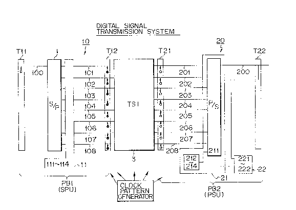
Figure 1 is a block diagram of a typical and
conventional digital signal transmission system having
monitor equipment and Figure 2 is a timing chart
explaining the operation of the system shown in Fig. 1.
Referring to both Figs. 1 and 2, reference numeral 1
represents a serial/parallel (S/P) converter to which a
serial signal is input via a multiplexed channel
line 100. The serial signal is shown in row (B) of
-4 2~69284
Flg. 2. The serial signal of row (B) is converted into
parallel signals shown in row (C) of Fig. 2, parallel
signals of which are distributed to respective individual
channel lines 101 through 108.
The S/P converter 1, the multiplexed channel line
100 and individual channel lines 101 through 108 are
usually loaded on the same printed board PB1 for the S/P.
The aforesaid serial signal of row (B) in Fig. 2 is input
from an input terminal T11 mounted on the above printed
board PB1. The aforesaid parallel signals of row (C) in
Fig. 2 are output from output terminals T12 mounted on
the above printed board PB1.
Each serial signal given from the input terminal T11
is a digital signal multiplexed as shown in row (B) of
lS Fig. 2. Each serial digital signal is composed in the
form of a frame as usual. That is, each frame is
composed of a time slot as shown by CH1, CH2, CH3 ... as
shown in row (A) of Fig. 2. Note that the digital signal
on each of these time slots corresponds to respective
channels, and thus the time slots are expressed as the
channels CH1, CH2, CH3 ....
The channels CH1, CH2, CH3 ..., i.e., the time
slots, are composed of 8 bits, respectively, as shown in
row (B) of Fig. 2. Namely, the channel CHl is composed
of an 8-bit signal with bit al through bit a8.
Similarly, the channels CH2 and CH3 are composed 8-bit
signals with bit bl through b8 and bit cl through c8,
respectively.
Since each time slot is composed of 8 bits,
8 parallel signals are produced as shown in row (C) of
Fig. 2. For this, 8 individual channel lines 101
through 108 are provided to match with the 8 bits, as
illustrated in Fig. 1.
The parallel signals from the S/P converter are
applied to a time slot interchanger (TSI) 3 located at
the center of the digital signal transmission system,
wherein an interchange between the two channels (two time
- - 20~9284
slots) is performed.
The interchange is performed between, for example,
the channel C~1 and the channel CH2 as seen at the
portion between rows (C) and (D) of Fig. 2 by means of
the interchanger (TSI) 13. Thus the parallel bits al
through a8 and bl through b8 of row (C) are interchanged
to the parallel bits bl through b8 and al -through a8 of
row (D)-
The thus interchanged parallel signals from the time
slot interchanger (TSI) 3 are distributed to respective 8individual channel lines 201 through 208, as shown in
Fig. 1, to reach a parallel/serial (P/S) converter 2,
wherein the parallel signals are converted again into a
serial signal as shown in row (E) of Fig. 2 and then
output on a multiplexed channel line 200. The serial
signal of row (E) corresponds to a multiplexed digital
signal obtained by interchanging the serial signal of row
(B) input to the S/P converter 1, between the
channels CHl and CH2, at the interchanger (TSI) 3.
The P/S converter 2, the multiplexed channel
line 200 and the individual channel lines 201 through 208
are usually loaded on the same printed board PB2 for the
P/B, as in the printed board PB1. The aforesaid parallel
signals of row (D) in Fig. 2 are input from input
terminals T21 mounted on the board PB2. The aforesaid
serial signal on the line 200 is output from an output
terminal T22 mounted on the same board PB2.
Incidentally, the time slot interchanger (TSI) is mounted
on a similar printed board (PB) dedicated thereto.
Figure 3 is a block diagram explaining an operation
that is equivalent to the operation of the system shown
in Fig. 1. The system of Fig. 1 can be expressed
generally as an exchange. The exchange has, as its major
part, a switching network that is equivalent to the
aforesaid time slot interchanger (TSI) 3. The incoming
and outgoing lines, as the aforesaid highway transmission
line, operate at, e.g., 6 Mbps, while, the internal
206~28~
circuit of the exchange operates at a higher speed than
the incoming and outgoing lines, e.g., 8 Mpbs, in order
to gain an operational margin. In order to adjust the
difference in speed, frame aligners are needed.
Referring again to Figs. l and 2, when a fault
occurs in the system of Fig. 1, the electronic circuits
on the aforesaid printed boards (PB) are monitored
individually. To be specific, the electronic circuit of
the printed board mounting the interchanger (TSI) 3 is
monitored by the use of a well known parity check, since
the interchanger (TSI) primarily consists of ~ random
access memory (RAM). In general, a memory circuit is
suitable for the parity check. On the other hand, the
electronic circuits of the printed boards PBl and PB2
mounted on the S/P and P/S converters are monitored by
the use of a pass pattern check.
In this case, it is possible for the interchanger
(TSI) 3 to be monitored even inside thereof. Contrary to
the above, as previously mentioned, the inside of the S/P
and P/S converters 1 and 2 cannot be monitored.
Therefore, the pass pattern check is applied, on the
printed board PB1, to the electronic components other
than the S/P converter 1. Also, the pass pattern check
is applied, on the printed board PB2, to the electronic
components other than the P/S converter 2. That is, the
pass pattern check is applied only to the multiplexed
channal line 100, the individual channel lines 101
through 108, the individual channel lines 201 through 208
and the multiplexed channel line 200, separately and
independently. It should be understood here that the
above lines are illustrated as simple lines in the
figures, but, in actuality, each line is provided with,
in series thereto, other electronic circuits, such as a
buffer, a noise filter and the like.
In Fig. 1, each small white circle with an arrow
indicates an input port to which the pass pattern signal
of the aforesaid pass pattern check is input, while, each
20~928~
small black circle with an arrow indicates an output port
from which the pass pattern signal of the aforesald pass
pattern check is output, the output pass pattern signal
of which is a signal to be monitored. ~ typical pass
pattern signal is composed of an alternative and
continuous "0" and "1" bit train.
Specifically, when the pass pattern check is
achieved on the printed board PBl, the pass pattern
signal is input to the input port at the input
terminal T11 and then the thus input pass pattern si~nal
is taken from the output port at the input side of the
S/P converter l, whereby the multiplexed channel line can
be monitored. Similarly, the pass pattern signals are
input to the respective input ports at the output side of
the S/P converter 1 and then the thus input pass pattern
signals are taken from the output ports of the output
terminals T12, whereby the individual channel lines 101
through 108 can be monitored. The above operations are
also achieved on the printed board PB2. Namely, the pass
pattern signals are input to the input ports at the input
terminal T21 and then the thus input pass pattern signals
are taken from the respective output ports at the input
side of the P/S converter 2, whereby the individual
channel lines 201 through 208 can be monitored.
Similarly, the pass pattern signal is input to the input
port at the output side of the P/S converter 2 and then
the thus input pass pattern signal is taken from the
output port at the output terminal T22. If the output
pass pattern matches with the input pass pattern
("01 01 01 ... "), it is determined that no fault occurs
on and along the path through which the pass pattern
signal has travelled.
As mentioned above in detail, according to the prior
art monitor equipment, the S/P and P/S converters 1 and 2
per se are not monitored. Further, as understood from
many input ports and output ports of Fig. i, there is an
increase in the amount of hardware of monitor equipment.
2~928~
The above problems of the prior art can be overcome
by introducing a means that enables the pass pattern
signal to pass through the S/P converter 1 and the P/S
converter 2.
S Figure 4 is a principle construction view of a
digital signal -transmission system including monitor
equipment according to the present invention. Note that
identical constituent members are represented by the same
reference numerals and symbols throughout the figures.
As seen from Fig. 1, the monitor equipment of the
present invention is basically comprised of a first
monitor means 10 and a second monitor means 20.
The first monitor means 10 for receiving parallel
pass pattern signals passing through the S/P converter 1
and converting the same after conversion into a serial
pass pattern signal, into plural sets of serial pass
pattern signals to be applied parallel to respective
individual channel lines 101 to 108 to achieve a S/P
convexter side pass pattern check.
The second monitor means 20 for receiving respective
serial pass pattern signals sent via respective
individual channel lines 201 to 208 and distributing each
serial pass pattern signal through the P/S converter 2 to
the multiplexed channel line 201 to 208 sequentially,
frame by frame, to achieve a P/S converter side pass
pattern check.
The first monitor means 10 is operative, on the
printed board PB1, as follows. The serial signa~ as well
as the serial pass pattern signal is applied to the input
port at the input terminal T11 as in the prior art.
The first monitor means 10 cooperates with the
existing S/P converter 1 and processes the output from
the S/P converter 1 by a first monitor signal generating
circuit 11 that generates parallel distributed serial
pass pattern signals. The first monitor means 10 finally
achieves a monitor of the pass pattern signals output
from the output ports at the output terminal T12, as in
20~8~
g
the prior art, however, the pass pattern check according
to the present invention is adopted not only for the
lines 100 and lO1 to 108, as in the prior art, but also
the S/P converter 1 per se. Thus, one of the aforesaid
problems can be overcome.
The second monitor means 20 is operative, on the
printed board PB2, as follows. The parallel signals as
well as the respective serial pass pattern signals are
applied to respective input ports at the input
terminal T21 as in the prior art. The second monitor
means 20 is mainly set up by a second monitor signal
generating circuit 21 and a pass pattern monitor
circuit 22. The circuit 21 includes therein the existing
P/S converter 2 to convert the serial pass pattern
signals received from respective individual ~hannel
lines 201 to 208 into serial pass pattern signals to be
output sequentially, frame by frame, on the multiplexed
channel line 200. The sequential serial pass pattern
signals are applied to the pass pattern monitor
circuit 22 to sequentially achieve the pass pattern
checks for each individual channel line 201 to 20~3. Thus
the pass pattern check according to the present invention
is adopted not only for the lines 201 to 208 and 200, as
in the prior art, but also the P/S converter 2 per se.
This overcomes one of the aforesaid problems.
In other words, the first means 10 including the S/P
converter 1 can be expressed as a serial/parallel
converting unit (SPU) and similarly the second monitor
means 20 including the parallel/serial converter 2 can be
expressed as a parallel/serial converting unit (PSU)
(refer to characters "SPU" and "PSU" in Fig. 4).
The operation will be explained in more detail
below. In the SPU of Fig. 4, the serial pass pattern
signal is input to the input terminal T11 and is
converted, gradually into parallel pass pattern signals
by the S/P converter l. The parallel pass pattern
signals are applied to the first monitor signal
2~6928~
-- 10 --
generating circuit 11 to produce, first, serial pass
pattern signals by sampling each parall~l pass pattern
signal sequentially at the same S/P conversion speed of
the S/P converter 1 and then the thus sampled parallel
pass pattern signals are multiplexed into plurality sets
of serial pass pattern signals to be distributed parallel
on respective individual channel lines 101 to 108. On
the other hand, in the PSU of Fig. 4, the second monitor
signal generating circuit 21 receives each serial pass
pattern signal given from respective individual channel
lines 201 to 208 and the respective serial pass pattern
signals are sequentially output, individually on the
multiplexed channel line 200. The pass pattern monitor
circuit 22 achieves the pass pattern checks for each
serial pass pattern signal sequentially frame by frame
cyclicly.
Figure 5 is a circuit diagram of an example of a
first monitor signal generating circuit 11 shown in
Fig. 4 and Figure 6A and 6B is a -timing chart explaining
the process of a generation of the first monitor signal.
In Fig. 5, the serial pass pattern (P-P) signal pl
to p8 (see row (B) of Fig. 6A) is input to the
terminal T11 and reaches, via the line 100, the S/P
converter l, as well as the usual serial signals, such
as al to a8, bl to b8 and so on.
The serial P.P signal is applied to the terminal T11
every time a dummy time slot (TS) comes (see DUMMY TS in
row (A) of Fig. 6A), in the form of 8 bit train pl to p8.
Note that each dummy time slot is necessary to adjust the
difference in speed between, e.g., 6 Mbps and 8 Mbps (see
Fig. 3), in which no usual data signal exists.
The S/P converter 1 converts the serial signals of
row (B) in Fig. 6A to parallel signals as shown in rows
(C-1) to (J-l) of Fig. 6A and 6B. During the S/P
conversion, the serial pass pattern (P-P) signal pl to p8
of row (B) is converted, gradually into 8 parallel P-P
signals (see pl (C-1), p2 (D-1), p3 (F-1), p4 (F~l) --
2~6928~
11
p8 (J-1). These parallel P-P signals are input to the
first monitor signal generating circuit 11.
The first monitor signal generating circuit 11
consists of a pass pattern extracting circuit 111, a pass
pattern multiplexing circuit 112 and a timing control
circuitry such as a frame counter (FRAME COUNT) 113, a
decoder ( DEC) 114.
The frame counter 113 receives a frame pulse signal
and a clock (CLK) signal supplied from a clock pattern
generator (see Fig. 4), to thereby generate a timing
trigger necessary for producing gate signals (see rows
C-2, D-2, E-2 ... J-2) and a timing trigger necessary for
producing the timing signal (K) that specifies the time
slot ("DUMMY TS") during which the parallel pass pattern
signals (C-1, D-l, E-l ... J-l) should be sampled to
generate the serial P-P signal (see pl to p8 in row (L),
(M) -. (S)).
The above mentioned timing triggers are supplied to
the decoder 114 to produce the above mentioned gate
signals (C-2, D-2, E-2 ... J-2) and timing signal (K).
The pass pattern (P-P) extracting circuit 111
consists of AND gates 111-1 and an OR gate 111-2. The
AND gates 111-1 are arranged in individual correspondence
with the output bits of the S/P converter 1. The OR
gate 111-2 multiplexes the outputs from the AND
gates 111-1.
Namely, the serial P-P signal pl to p8 of row (B) is
reproduced by taking an AND operation at each AND gate
(111-1) between the serial P-P signal from the S/P
converter 1 and the respective gate signals (see row
(C-2), (D-2) ... (J-2)) each having a bit width of the
bits pl to p8 in row (s).
The pass pattern multiplexing circuit 112 consists
of the same number of selectors as the number of channel
lines 101 and 108. The selectors receive respective
parallel signals from the S/P converter 1 respectively
and also receive the output signal from the pass pattern
- 12 - 2~92~4
extracting circuit 111 commonly. Further the selectors
are commonly supplied with the timing signal (shown in
row (K) of Fig. 6B) from the decoder (DEC) 114. Thereby,
the pass pattern multiplexing circuit 112 selectively
produces parallel signals, sùch as al to a8, bl to b8, cl
to c8 and so on, or the plurality sets of serial pass
pattern signals, each composed of pl to p8, at every term
when the timing signal (K~ is given, to be output to
respective individual channel lines 101 to 108.
The parallel distributed serial pass pattern signals
(see pl to p8 in rows (L), (M) ... (S) of Fig. 6B) are
monitored at respective output ports of the output
terminal T12 as in the prior art by the use of, e.g., a
pulse pattern comparator.
By employing the first monitor signal generating
circuit 11, the output port at the input side of the S/P
converter 1 and the input ports at the output side
thereof, which are necessary in the prior art, are no
longer needed by the monitor equipment of the present
invention.
Figure 7 is a circuit diagram of an example of the
second monitor signal generating circuit 21 and the pass
pattern monitor circuit 22 shown in Fig. 4 and
Figures 8A, 8B, 8C and 8D is a timing chart explaining
the operations performed in the circuit shown in Fig. 7.
In Fig.7, a bit counter (BIT COUNT) 212 receives a
time slot signal (see row (C) of Fig. 8A) and a bit clock
signal (CLK) (see row (D) of Fig. 8B) given from the
aforesaid clock pattern generator (Fig. 4) and achieves
an octal counting operation, and thereby bit address
signals (QAI Q~l QC) are produced therefrom as seen in
rows (E), (F) and (G) of Fig. 8B. The bit address signal
QA is the least significant bit (LSB) of the output of
the bit counter 212, and the bit address signal QC is the
most significant bit (MSB) thereof.
These bit address signals QAI Q~ and Qc are applied,
- 13 - 20692~4
via a selector 214, to a selectable parallel/serial (P/S)
converter 211 that includes an inherent function of the
aforesaid P/S converter 2. The selectable P/S
converter 211 converts the parallel signals (see al to
a8, bl to b8, cl to c8 ... shown in rows (B-1) to (B-8)
of Fig. 8A) se~uentially accordin~ to each combination of
the bit address signals QA~ QB and Qc, into the serial
signals (see al to a8, bl to b8 and so on as shown in
rows (B-1) to (B-8) of Fig. 8C).
For example, if the bit address signals QAI QB and QC
assume "000", the parallel signal al in row (B-1) of
Fig. 8A is selected. Similarly if "100' is given, a2 of
row (B-2) is selected. Thus, if the QAr QB and QC assume
a 3 bit logic on the left side, the right side parallel
signals are selected as shown below.
'010' - a3 (row (B-3) of Fig. 8A)
"110" - a4 (row (B-4) of Fig. 8A)
"001" - a5 (row (B-5) of Fig. 8A)
"101" - a6 (row (B-6) of Fig. 8A)
011" - a7 (row (B-7) of Fig. 8A)
'111" - a8 (row (B-8) of Fig. 8A)
The thus selected parallel signals are multiplexed
to be the serial signals al to a8 at the channel CH1 as
seen in row (B-1) of Fig. 8B. Similarly, the parallel
signals are multiplexed to be the serial signals bl tG b8
and cl to c8 and so on at the channel CH2 and CH3,
respectively as shown in row (B-1) of Fig. 8C.
The pass pattern signals pl to p8, ql to q8 ... are
treated as follows. The serial pass pattern signals
30 applied to the individual channel lines 201 to 208 are
sequentially output frame by frame to the multiplexed
channel line 200 in the form of a multiframe system by
means of the selectable P/S converter 211 and the frame
counter 213.
To facilitate an understanding of the frame and the
multiframe, Fig. 8C is referred to. Each of the serial
2~9284
- 14 -
pass pattern signals is composed of 8 bits as shown in
rows (B-1) to (B-8) of Fig. 8A, and therefore, each
multiframe (see row (F) of Fig. 8D) is composed of 8
frames F1, F2 ... F8 as seen in row (H) of Fig. 8D. The
frame train Fl, F2 ... F8 can be schematically
illustrated as shown in row (G) of Fig. 8D, where the
dummy time slot in which the serial pass pattern signal
is inserted is assumed to be positioned at each end part
of the frames (F1, F2 ... F8) as opposed to the location
of the serial pass pattern signals (pl to p8, ql to q8
...) shown in Fig. 8A, since each frame is usually
composed of, e.g., CH1, CH2, CH3 ... CH30.
In row (G) of Fig. 8D, the bit concentrations of
each serial pass pattern signal (pl to p8, ql to q8 ...
wl to w8 in Fig. 8A) are expressed schematically as each
set of vertical short lines at each end part of the
frames.
In Fig. 7, the frame counter 213 consists of, e.g.,
an octal counter. The octal counter (213) is supplied
with the multiframe signal and the frame signal both from
the aforesaid clock pattern generator shown in Fig. 4.
In response to the multiframe and frame signals, the
frame counter (FRAME COUNT) 213 produces the frame
address signals QA', QB' and QC' as shown in row (B), (C)
and (D) of Fig. 8D; the frame address signals are applied
to the selector (SEL) 214. Thus the selector 214
receives the bit address signals QAI QB and QC from the
bit counter 212 and the frame address signals QA' ~ QB'
and QC ' from the frame counter 213 and either one of the
two sets of signals are selected by the address selection
signal of row (E) in Fig. 8D, the signal of which is also
supplied from the aforesaid clock pattern generator shown
in Fig. 4.
Namely, the address selection signal indicates each
timing corresponding to the occurrence of the dummy time
slot (DUMMY TS) in which the serial pass pattern signals
2~9284
- 15 -
are inserted. Every time the address selection signal is
generated (refer to each negative pulse shown in row (E)
of Fig. 8D), the selector (SEL) 214 is switched to select
the frame address signals QA' QB' and Qc'- At this time,
the selectable P/S converter 211, when receiving the
signals QA~ I QB~ and QC', operates to produce the serial
pass pattern signal, e.g., pl to p8 of row (B-1) in
Fig. 8C during a certain frame. During the next frame,
the converter 211 produces, when receiving the next
signals QA' I QB' and QC~ the serial pass pattern signal,
i.e., ql to q8. The same operation will continue
synchronously with the frame.
To be more specific, if the selectable P/S
converter 211 receives, as the combination of the frame
address signals QA', QB' and Qc'~ "000", "001", "010",
"010", "100", "101", "110" and "111", the P/S
converter 211 produces respectively the serial pass
pattern signals pl to p8 (row (B-1) of Fig. 8C), ql to q8
(row (B-2) of Fig. 8C) and so on along with the advance
of the frame. These serial pass pattern signals are
sequentially applied, via the line 200, to the pass
pattern monitor circuit 22. It should be noted that, in
Fig. 8C, only the bit patterns at the dummy time slot are
completely depicted for brevity.
The serial signals, including the serial pass
pattern signals, are sent from the circuit 21 to the
line 200. Among the serial signals, the serial pass
pattern signals are checked through the output
terminal T22 by the pass pattern monitor circuit 22. The
circuit 22 consists of a serial/parallel converter for a
monitor 221 and a pass pattern comparator 222.
The serial signals are branched at the output
terminal T22 and applied to the pass pattern
comparator 222 after conversion into parallel signals at
the S/P converter for monitor 221.
The pass pattern comparator 222 receives the
- 16 - 2~S~28~
aforesaid frame address signals QA' I QB' and QC' and, in
response to the combination of these signals QA' / QB' and
QC' , only the pass pattern signals, pl to p8, ql to q8
... wl to w8, are checked sequentially with reference to
the corresponding reference pass patterns. The reference
pass patterns are the same as the respective pass
patterns that are input to the input terminal T21.
Example of the pass patterns is shown below.
pl to p8 : 0 l 0 1 0 1 0
ql to q8 : 1 0 1 0 1 0 1 0
rl to r8 : 0 0 1 1 0 0
sl to s8 : 1 1 0 0 l l 0 0
tl to t8 : 0 0 0 0
ul to u8 : 1 1 1 1 0 0 0 0
vl to v8 : 0 0 1 1 1 l 0 0
wl to w8 : l 1 0 0 0 0
Fig. 9 is a circuit diagram of an example
representing the selectable P/S converter 211 of Fig. 7.
The selectable P/S converter 211 can be constructed as
an 8-line to 1-line data selector/multiplexer. Reference
symbols D0 through D7 denote bit data.
As explained above in detail, the monitor equipment
of the present invention enables a monitor of both the
SJP converter 1 per se and the P/S converter 2 per se of
the digital signal transmission system, and thus the
reliability of the system can be greatly improved.
Further, the amount of hardware for constructing the
input ports and the output ports can be halved when
compared with the prior art, thereby reducing the
manufacturing cost.