Note: Descriptions are shown in the official language in which they were submitted.
The present invention relates to a method and a
device for digital bidirectional data transmission on an
optical waveguide connecting two transmitter/receiver units
with one another.
The simplest prior art method of a bidirectional
data transmission over optical waveguides includes a
separate optical waveguide ~or each direction of
transmission. This approach is disadvantageous in that it
increases the cost for long-distance communications, due
to the employment and laying of one optical waveguide for
each direction of transmission.
Further, there is known in the art a wavelength-
division multiplexing method, wherein different wavelengths
(or frequencies) are used for each direction of
transmission. ~ wavelength ~1 = 1,300 nm can be used, e.g.,
for the one direction, and ~2 = 1,550 nm for the other
direction. By using different wavelengths of the
transmitting light, the transmission of both directions can
be performed on a signal optical waveguide. Each of the
two transmitter/receiver units must include a wavelength-
selective component (multiplexer), being used for the
separation o~ the two wavelengths. If the difference of
the two wavelengths ~ 2 - ~1 is within the bandwidth of
the sensitivity of the employed optical receivers, it is
not necessary to discriminate between the two wavelengths
in the optical receiver. It is disadvantageous, in this
case, that the wavelength-selective elements have to
provide a high selectivity or attenuation, such that only
very good multiplexers having a high wavelength isolation
can be used. These are very expensive. Moreover, proper
communication over long distances will require an
attenuation of at least 50 db between the two channels, in
order to avoid cross-talk between the channels.
Another prior art method is the packet-switched
data transmission, wherein, over a single optical
waveguide, alternatingly for both directions, the data are
:, ~ - . . .
6 ~
transmitted in the form of packets. At the beginning and
at the end of each packet, a start or stop information for
control and monitoring of the transmission is inserted.
After the stop information associated with a data packet is
received and evaluated at the actual receiver side, the
transmitter can, in the opposite direction of the
transmission path transmit its data as a packet provided
with respective start and stop information. It has to be
considered, therein, that a long pause is to be maintained
between two packets, which has, due to the transmission
time, to be at least as long as the transit time over the
transmission path. It is disadvantageous, herein, that due
to the long pauses, the transmission path cannot be
utilized in an optimum manner. Moreover, the packet-
switched transmission method requires an expensive clockrecovery, large data rates and a complicated control
system. Depending on the length of the packets, a large
memory may also be necessary.
The present invention is based on the object,
therefore, to provide a simple and economic method for the
optical, bidirectional data transmission on an optical
waveguide which operates on one light frequency only and
which avoids the prior disadvantages.
According to an aspect of the present invention,
there is provided a method for bidirectional, digital data
transmission on an optical waveguide having respective
first and second transmitter/receiver units at either end,
wherein: transmission of the data flow for either direction
is performed simultaneously and at the same fre~uency for
the optical signals; the optical signals have a pulse width
Tr which is reduced relative to the pulse width Tb of the
signals to be transmitted, the ratio Tr/(Tb - Tr) being
smaller than one; and the second transmitter/receiver unit
transmits a pulse-width-reduced signal Tr to the first
transmitter/receiver unit only in a reception pause (Tb -
Tr) ~
2~6~
According to the invention, transmission of the
data flow for either direction is performed simultaneously,
the same light wavelength being applied for either
direction~ In order to avoid the problem of decoupling of
transmitter and receiver of the same transmitter/receiver
unit, which occurs when using optical signals of the same
wavelengths for the bidirectional transmission on an
optical waveguide, the original pulse width Tb of the
signals to be transmitted is reduced, for the optical
transmission, to a smaller pulse width Tr. This corresponds
to a RZ coding, the pulse-to-pause ratio Tr/(Tb - Tr) being,
according to the invention, smaller than one. This pulse-
width-reduced signal of the length Tr is transmitted, over
the optical waveguides, from the first to the second
transmitter/receiver unit and is fed there to a second
receiver. Then, a pulse~width correction is performed, so
that the data pulse again receives its original width Tb.
Thereby, at the second transmitter/receiver unit a
reception pause (Tb - Tr) results, which can be used, by the
second transmitter, for transmitting a pulse reduced to the
pulse width Tr~ in the direction of the first
transmitter/receiver unit. The second transmitter
transmits, therefore, only in the so-called reception pause
(Tb -- Tr) -
For certain light wavelengths this will lead, at
the first receiver, to an optimum timing between the
signals of the two transmitter/receiver units. For other
transmission lengths of the optical waveguides, there is a
possibility that the signals from the first and second
transmitters will superimpose each other, so that crosstalk
will result.
In order to avoid this, the first transmitter/
receiver unit monitors the pulse timing on the optical
~aveguide, and causes, if necessary, the second
transmitter/receiver unit, by means of a modify signal, to
change its transmission time within the reception pause.
- 2 ~ B
~
This modification of the transmission time at the second
transmitter is made, until an optimum timing between the
signals of the two transmitters is achieved at the first
transmitter/receiver unit. We have here, therefore, a
feedback control loop. The transmission of the modify
signal can be performed at any place within the data flow,
or it can be provided, for the transmission, an own time
slot.
In a further advantageous embodiment, the
receiver-side data processing is stopped in a
transmitter/receiver unit, if the respective transmitter
transmits an optical signal. Thereby, crosstalk is
avoided, or faded out.
The decision, whether or not a signal timing is
favourable, can be performed by a measurement of the bit
and/or code error of the transmission.
In the following, the invention is described in
more detail, based on a preferred embodiment represented in
the drawings. There are:
Figure 1 is a schematic block diagram of a
bidirectional data transmission on an optical waveguide;
Figure 2 is a more detailed block diagram of a
bidirectional data transmission;
Figure 3 is a block diagram of a device according
to the invention, together with the components thereof;
Figure 4 is a pulse distribution diagram for an
optimum distribution of the signals; and
Figure 5 is a pulse distribution diagram for
different transmission times of the return pulse.
Referring now to Figure 1, the connection between
a first transmitter/receiver unit 1 with a second
transmitter/receiver unit 2 through an optical waveguide 3
is shown. Data transmission takes place simultaneously in
either direction, i.e. bidirectionally, and the employed
frequency of the optical transmission pulses is identical
for either direction.
Figure 2 shows the fundamental construction of
the transmitter/receiver units 1, 2 in greater detail. The
transmitter/receiver unit 1 comprises a first transmitter
unit 4 and a first receiver unit 5 By means of a first
coupling element 6, data from the first transmitter unit 4
are transferred to the optical waveguide 3, or data from
the optical waveguide 3 are conducted into the receiver
unit 5. The second transmitter/receiver unit 2 comprises
analogous components, second receiver unit 7, second
transmitter unit 8 and an optical coupling element 9 for
coupling data into or out from the optical waveguide 3,
respectively.
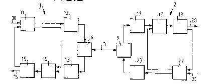
A block diagram of a preferred embodiment for
implementing the method according to the invention is shown
in Figure 3. On either side of the optical waveguide 3,
there are provided the transmitter/receiver units 1 and 2.
The first transmitter unit 1 comprises a data input 10,
conducting the digital data to be transmitted and having
the pulse width Tb into a data editing unit 11. In the data
editing unit 11, the pulse width is reduced from the
original width Tb to the reduced width Tr. These width-
reduced pulses are fed to a first optical transmitter 12
generating optical transmission pulses having the length Tr~
corresponding to the electrical pulses. By means of the
optical coupling element 6, the optical transmission pulses
are transferred to the optical waveguide 3. Optical pulses
coming from che second transmitter/receiver unit 2 are
conducted, by the second optical coupling element 6, into
an optical receiver 13 and are transformed, therein, into
electrical signals having the pulse widths Tr. The
transformed pulses arrive at a pulse-width correction unit
14, widening the pulses back to their original pulse widths
Tb. To the pulse-width correction unit 14 is fed the output
signal of the data editing unit 11, so that at times when
the optical transmitter 12 transmits with the pulse
duration Tr~ the pulse-width correction unit 14 is blocked
~9~
or switched off. Thereby, crosstalk between outgoing
optical signals of the transmitter/receiver unit 1 and any
incoming siynals of the transmitter/receiver unit 2 is
avoided. The pulse-width-corrected data arrive at a bit-
code error measurement unit 15, serving for detecting anunfavourable timing between the transmitted and received
optical signals. If the measurement yields a positive
result, the valid data are transferred to a data output 16.
If not, a modify signal is transferred, over a connection
of the bit-code error measurement unit 15 with the data
editing unit 11 and the coupling element 6, to the optical
waveguide 3, effectiny a modification of the time behaviour
of the second transmitter/receiver unit 2.
The second transmitter/receiver unit 2 comprises
an optical coupler 9, coupling the optical signals o~ the
optical waveguide 3 in or out, respectively. Incoming
optical signals are supplied from the optical coupling
element 9 to an optical receiver 17, transforming the
optical signals having the lengths T, into signals having
identical lengths. The transformed signals are fed to a
pulse-width correction unit 18, widening the pulses back to
their original lengths Tb. The subse~uent control signal
output unit 19 serves for separating control signals from
the data flow, in particular the modify signal. Valid data
are fed to the data output 20. The recognized control
signals are supplied to the data editing unit 22, together
with the data input 21. The data editing unit 22 modifies,
depending on the control signals of the control signal
output unit 19, the signal timing, i.e. the time of
transmitting a signal in the reception pause, and reduces
the pulse width of the data from the original width Tb to
T,. The electrical signals are fed, on one hand, to an
optical transmitter 23, performing an electro-optical
transformation of the signals, and simultaneously, the
transmission signal i5 fed to the pulse-width correction
unit 18. During transmission of a signal, therefore, the
. .
: . ,
~9~6~
pulse-width correction unit 18 is blocked, so that
crosstalk of the two optical transmitters is faded out.
The optical coupler g coupl~s the transmission signal onto
the optical waveguide 3.
Figure 4 shows an optimum distribution of the
optical signals, i.e. optimum timing, on the optical
waveguide 3. Horizontally, the glass-fibre length, and
vertically, the pulse amplitude are shown. The
distribution is represented for an arbitrary, but fixed
time t = t1. The upper portion of Figure 1 contains the
direction of the transmitter/receiver unit 1 to the
transmitter/receiver unit 2, whilst the lower portion
contains the opposite direction. On the upper horizontal
axis, reference numeral 24 marks the location of the
optical transmitter 12, and reference numeral 25 the
location of the optical receiver 17, on the optical
waveguide 3. In an analogous manner, on the lower
horizontal axis, reference numeral 26 marks the location of
the optical receiver 13, and reference numeral 27 the
location of the optical transmitter 23, on the optical
waveguide 3. The pulses have reduced widths Tr. The
original pulse width Tb is given, in Figure 4, by the
spacing of the first leading edge of a pulse to the leading
edge of the following pulse. An optimum signal
distribution is achieved, when the pulse in the return
direction, here shown by the lower portion of Figure 4, is
approximately in the middle of the reception pause (Tb -
T,).
Figure 5 shows schematically, how the optical
pulse outgoing from the transmitter/receiver unit 1 can be
displaced in time relative to a pulse of the direction
transmitter/receiver unit 1 to transmitter/receiver unit 2.
In the horizontal direction is displayed the glass-fibre
length, and in the vertical direction the pulse amplitude.
Each upper portion of the four diagrams is the transfer
direction from the first optical transmitter 12 to the
2~9~6~
second optical receiver 17, and each lower portion the
transfer direction from the second optical transmitter 23
to the first optical receiver 13. On the horizontal axes
are further shown the location of the optical transmitter
24, the location of the second optical receiver 25, the
location of the first optical receiver 26 and the location
of the second optical transmitter 27. The situation in the
direction of transmission 12 to 17 is identical on all four
diagrams, namely that at the location of the second optical
receiver 25, the leading edge of an optical transmission
pulse Tr just occurs. The spacing between the two leading
edges of the shown transmission pulses is the original
pulse width Tb, as in Figure 4. The lower portions of the
four diagrams each show that due to the "modify signal",
the location of the return pulses with respect to time and
thus also with respect to location is relatively displaced.
Between the transmitter/receiver unit 1 and the
transmitter/receiver unit 2, there is a master-slave
relationship, i.e. the master (transmitter/receiver unit 1)
decides, whether or not the timing behaviour of the optical
pulses on the optical waveguide 3 is favourable in either
direction, and causes the slave (transmitter/receiver unit
2), by means of a modify signal, to modify the time of its
transmitted optical signal in the reception pause (Tb - Tr~.
The decision, whether a timing is favourable or un-
favourable, is performed by a bit-code error examination.
Therefore, a control loop is established, wherein the
timing is modified, until the measurement at the
transmitter/receiver unit 1 delivers an optimum timing of
the transmission pulses.