Note: Descriptions are shown in the official language in which they were submitted.
c~
CFO 8476 ~
209702
_ 1
1 Micro-displacement Element, and Scanning
Tunneling Microscope and Information
Processing Apparatus Using Same
BACKGROUND OF THE INVENTION
Field of the Invention
The present invention relates to a micro-
displacement element comprising a unimorph cantilever,
as well as a scanning tunneling microscope (STM) and a
large-capacity and high-density information processor
using the micro-displacement element.
Related Background Art
In recent years, there has been the tendency
that the data recording capacity in an information
processor is being increased year by year, while the
size of a recording unit is miniaturized and thus the
recording density is heightened. For example, in a
digital audio disk in which an optical recording
system is utilized, the size of a recording unit is as
small as 1 ~m2 or so. In the background of these
facts, there is the active development of memory
materials, and in consequence, inexpensive and high-
density recording media using organic thin films of
organic dyes, photopolymers and the like have come
out.
On the other hand, the STM has recently been
developed by which the electronic structure of surface
_ 2
1 atoms of a conductor can be directly observed [G.
Binning et al., Helvetica Physica Acta, 55, 726
(1982)], and as a result, the real space image can be
measured with a high resolution irrespective of a
single crystal or an amorphous substance. In addition,
observation can be advantageously made at a low
electric power without damaging a medium with current.
Moreover, the STM can be operated even in the atmosphere
and can be applied to various materials, and for these
reasons, it is expected to employ it in many fields.
The STM utilizes the phenomenon that when a
voltage is applied to between a metallic probe (a
probe electrode) and a conductive material and the
probe is then brought close to a position about 1
nanometer distant from the conductive material, a
tunnel current flows therebetween. This current is
very sensitive to a distance change between them, and
therefore the surface information of the real space
can be obtained by scanning a probe so as to constantly
maintain the current or the average distance between
them. In this case, the resolution in the surface
0
direction is about 1 A.
If the principle of this STM is utilized, a
high-density recording, and reproduction can be
sufficiently achieved in an atomic order (several
angstroms). In this case, as recording reproduction
methods, there have been suggested, for example, a
206'702
- 3 -
1 method which comprises changing the surface state of
a suitable recording layer by the use of a particle
beam (an electron beam or ion beam), or an energy beam
including a high-energy electromagnetic wave such as
X-ray and a visible or ultraviolet light, for
recording information, and then reproducing it by the
STM; and a method in which a material exhibiting a
property of switching voltage-current characteristic
with a memory effect, for example, a thin film of a ~r
electron type organic compound or a chalcogen compound
is used as the recording layer, and recording and
reproduction are carried out by using the STM (Japanese
Patent Appln. Laid-Open No. 63-161552 and the like).
In the information processor utilizing the STM,
it is important to control the distance between a
probe and a recording medium in an angstrom order. In
addition, it has been suggested to simultaneously
drive many probes (multiplication of the probe) from
the viewpoint of the function improvement of a
recording/reproduction system, particularly a high-
speed processing.
For this control, a lamination type piezo-
electric element, a cylindrical piezoelectric element
and the like attached on the probe or the medium have
been heretofore used (U. S. Patent No. 4668865).
However, these elements are not suitable for
integration, though the use of them permits obtaining
2U~~'~~2
- 4 -
1 a large displacement. Thus, it is inconvenient to use
these elements in the multi-probe type information
processor. In view of this standpoint, a method has
been contrived in which a probe is attached on a
cantilever having a length of about several hundreds
um, and this cantilever is then driven by a piezo-
electric element.
Figs. 9 and 10 show an example in which a
cantilever comprising a piezoelectric bimorph is
formed on an Si substrate [Thomas R. et al., J. Vac.
Sci. Technol., A8, p. 317, 1990]. Fig. 9 is its
perspective view, and as shown in this drawing, a
cantilever is formed on an Si substrate 1 by laminating
two-divided lower electrodes 3, a Zn0 piezoelectric
thin film 904, a medial electrode 902, a Zn0 piezo-
electric thin film 904 and two-divided upper electrodes,
and a portion of the Si substrate under the cantilever
is then removed by anisotropic etching so that the
cantilever is held to be overhung from the edge of the
Si substrate.
The cantilever comprising this piezoelectric
bimorph is provided on the tip thereof with a metallic
probe 6, which detects a tunnel current through an
outgoing electrode. In this case, when voltages are
independently applied to the four regions including
two piezoelectric regions sandwiched between the
upper electrodes 5 and the medial electrode 902 of the
2Q~~702
- 5 -
1 cantilever as well as two piezoelectric regions
sandwiched between the lower electrodes 3 and the
medial electrode 902 as shown in the sectional view of
Fig. 10, the cantilever having the probe 6 can be
independently moved.
However, when the cantilever having such a
piezoelectric bimorph structure as seen in the
conventional example is subjected to high-speed
scanning, inconvenient mechanical vibration called host
vibration is liable to occur on the cantilever, which
makes a correct image observation difficult.
Additionally, in the case that a plurality of
cantilevers are integrally arranged, there is a problem
that some of them bend owing to the internal stress of
the piezoelectric thin films or the electrode thin
films. This is considered to be attributable to the
ununiformity and the like of the piezoelectric thin
films and the electrode thin films at the time of the
formation of these films by a sputtering process or
a vapor deposition process.
For the writing or reading of information in
the information processor, it is necessary that all of
the respective cantilevers operate normally. When the
precision of these cantilevers is poor, an external
compensating operation and the like are required to
securing the precision.
In addition, since the cantilever takes the
20~~7~~
- 6 -
1 piezoelectric bimorph structure using the two piezo-
electric layers, many manufacturing steps are necessary,
which leads to the complication of the cantilever
formation. As a result, it is difficult to control
the stress of the thin films in the respective layers.
SUMMARY OF THE INVENTION
An ojbect of the present invention is to
provide a novel micro-displacement element by which
host vibration generated on a cantilever at the time
of high-speed scanning can be remarkably decreased
and by which image observation, recording and repo-
duction can be achieved with high precision and
reproducibility, and to provide an STM and an infor-
mation processor using the microdisplacement element.
Another object of the present invention is to
provide a multi-type micro-displacement element array
by which the bend and unevenness of plural cantilevers
arranged on one substrate can be reduced to the utmost
and by which image observation, recording and repro-
duction can be achieved with high precision and
reproducibility, and to provide an STM and an infor-
mation processor using the mufti-type micro-displace-
ment element array.
The above-mentioned objects can be accomplished
by the following present invention.
That is, the first aspect of the present
200702
1 invention is connected to a micro-displacement element
which comprises a unimorph cantilever having a piezo-
electric thin film, a pair of electrodes between which
the piezoelectric thin film is sandwiched and an
elastic thin film, one end of the cantilever being
supported by a support, the other end thereof being
provided with a probe for the input and output of infor-
mation.
The second aspect of the present invention is
connected to a multi-type micro-displacement element
array in which at least two of the above-mentioned
micro-displacement elements are arranged in a two-
dimensional state.
The third aspect of the present invention is
connected to a scanning tunneling microscope which
comprises the above micro-displacement element disposed
so as to face to an electrical conductor, a driving
means for driving the micro-displacement element, a
control means for controlling the driving means, a
means for applying a voltage to between the electrical
conductor and the probe, a means for detecting a tunnel
current which flows between the electrical conductor
and the probe, and a means for outputting an infor-
mation as to the surface of the electrical conductor
on the basis of the detection of a tunnel current.
The fourth aspect of the present invention is
connected to an information processing apparatus which
_ g _
1 comprises the above micro-displacement element disposed
so as to face to a recording medium, a driving means
for driving the micro-displacement element, a control
means for controlling the driving means, and a means
for applying an information recording pulse voltage
to between the recording medium and the probe.
The fifth aspect of the present invention is
connected to an information processing apparatus which
comprises a micro-displacement element disposed so as
to face to a recording medium, a driving means for
driving the micro-displacement element, a control means
for controlling the driving means, and a means for
applying an information reproducing bias voltage to
between the recording medium and the probe.
The sixth aspect of the present invention is
connected to an information processing apparatus which
comprises a micro-displacement element disposed so
as to face to a recording medium, a driving means for
driving the micro-displacement element, a control means
2~ for controlling the driving means, a means for applying
an information recording pulse voltage to between the
recording medium and the probe, and a means for applying
an information reproducing bias voltage between the
recording medium and the probe.
BRIEF DESCRIPTION OF THE DRAWINGS
Fig. 1 is a sectional view of a micro-
- 9 -
1 displacement element of the present invention.
Fig. 2 is a perspective view of the micro-
displacement element of the present invention.
Figs. 3A and 3B show the responsiveness of the
micro-displacement element of the present invention,
and Fig. 3A shows an applied voltage and Fig. 3B shows
a displacement.
Figs. 4A and 4B show the responsiveness in the
case that a bimorph cantilever is used, and Fig. 4A
shows an applied voltage and Fig. 4B shows a displace-
ment.
Fig. 5 is a perspective view of a multi-type
micro-displacement element array of the present
invention.
Fig. 6 is a sectional view of the micro-
displacement element of Example 2 of the present
invention.
Fig. 7 is a schematic view of the recording/
reproducing apparatus used in Example 2.
Figs. 8A to 8C show the characteristics of the
micro-displacement element of Example 4.
Fig. 9 is a perspective view of a conventional
micro-displacement element.
Fig. 10 is a sectional view of the conventional
micro-displacement element.
__-_ __-_ __.......-..-.~.-.r..~~~t n.~ rrnrrr~ r, r,rTrTr.TTTInT
L~7IIIDfITITMTa~TTTC
_ lp -
1 In the present invention, a cantilever-like
displacement element for giving a micro-displacement
is not formed so as to have a bimorph structure in
which two piezoelectric thin films are each sandwiched
between electrodes but so as to have a unimorph
structure which comprises an elastic thin film and
a single piezoelectric thin film sandwiched between
a pair of electrodes, whereby host vibration at a
high-speed operation can be decreased, the number of
steps at the time of manufacture can be reduced, and
multiple film formation steps which are liable to
accelerate uniformity in forming the thin films are
inhibited as small as possible.
Preferably, when a material having a linear
thermal expansion coefficient which is comparable to
that of the piezoelectric thin film is selected as
a material for the elastic thin film, the element
which is thermally stable and scarcely bends can be
obtained.
The reason for selecting such a material is
that it is necessary to perform the control in a
molecular/atomic order, i.e., in an order of several
nm, and when there is a temperature difference, the
cantilever tends to bend inconveniently by a bimetal
effect.
The preferable combination of the elastic thin
film and the piezoelectric thin film is such that the
209702
- 11 -
1 linear thermal expansion coefficients of both materials
are equal to each other, and at least the following
relation formula may be met:
(A - B) /A x 100 < 50 $
wherein A is the linear thermal expansion
coefficient of the material constituting the elastic
thin film, and B is the linear thermal expansion
coefficient of the material constituting the piezo-
electric thin film.
The typical examples of the combinations are
as follows:
Elastic thin film: Mg0 (A: 1.3 x 10 5/k) and
piezoelectric thin film: Zn0 (B: 1.5 x 10 5/k);
elastic thin film: Mo (A: 5.0 x 10 6/k) and
piezoelectric thin film: A1N (B: 5.0 x 10 6/k); and
elastic thin film: Si (A: 2.5 x 10 6/k) and
piezoelectric thin film: PbTi03 (B: 3.0 x 10 6/k).
The thickness of the elastic thin film is to be
about the same as that of the piezoelectric thin film,
and it is preferably in the range of 0.1 to 1.5 um.
The material of the elastic thin film may be organic
or inorganic.
Moreover, in the micro-displacement element
of the present invention, it is important that a
Young's modulus of the elastic thin film as a damper
(a brake material) is set in a suitable range. That
is, in the high-speed operation in STM, for example,
2~~~7~~
- 12 -
1 the displacement will overshoot, when a pulse voltage
is applied as a control voltage. This phenomenon is
considered to be attributable to the characteristic
frequency.
It is necessary that the Young's modulus of
the elastic thin film is set in the range of 1 x 10⁴
to 5 x 10¹¹ N/m2, preferably in the range of 1 x 10⁶
to 5 x 10⁸ N/m2.
In the above-mentioned information processor,
a sine wave, a triangular wave, a rectangular wave or
the like which is an alternating signal in a wide band
is used as a driving signal of the micro-displacement
element. Therefore, the disposition of the elastic
thin film permits removing unnecessary vibration.
Furthermore, a different deformation of a probe
can be independently made by additionally providing a
pair of electrodes on the cantilever in its crosswise
direction, which is a feature of the present invention.
In the case of the multi-type micro-displacement
element array, the respective cantilevers are precisely
formed, and as a result, high-quantity cantilevers are
manufactured in a high yield without forming warped
reject articles.
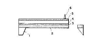
Fig. 1 shows a sectional view of the micro-
displacement element of the present invention, and Fig.
2 shows its perspective view.
An elastic thin film 2 is formed on an Si
20fi0'~02
_ 13 -
1 substrate 1, and on this elastic thin film 2, there
are laminated a lower electrode 3, a piezoelectric
thin film 4, an upper electrode 5 and a probe 6 in
this order. A plurality of such micro-displacement
elements are disposed on a same Si substrate, and an
electric field is applied to the piezoelectric
portions to drive the cantilevers, whereby reading
and writing are carried out by the use of a tunnel
current.
Now, the present invention will be described
in detail in reference to examples.
Example 1
Fig. 5 shows a schematic view of plural micro-
displacement elements.
Twelve (4 x 3 = 12) cantilevers 8 each com-
prising an elastic thin film and a piezoelectric thin
film having a pair of electrodes formed in the under-
mentioned steps are provided on an Si (100) substrate
1 having a size of 6 mm x 6 mm and a thickness of 0.3
mm, and a probe 6 for writing or reading of signals
is provided on each cantilever. With regard to the
size of each cantilever, its width is 100 um and its
length is 500 um.
The preparation method of each of the above
mentioned cantilevers will be described in reference
to Fig. 1. In the first place, an Si3N4 film having
a thickness of about 1500 A was formed as an elastic
2~6~'~~2
- 14 -
1 thin film 2 on an Si (100) substrate 1 (thickness
0.3 mm) by a CVD method. In this case, the Young's
modulus of this Si3N4 film was 2 x 10¹¹ N/m2. The
used gas was SiH2C12:NH3 = 1:9, and the film formation
temperature was 800°C. Next, the elastic thin film 2
was patterned in a desired shape by photolithography
0
and CF4 dry etching. Afterward, a Cr film of 50 A
0
and an Au film of 1000 A were formed thereon to
prepare a lower electrode 3, and patterning was then
carried out by photolithography and wet etching. Next,
a Zn0 film of 3000 A was formed as a piezoelectric thin
film 4 by a sputtering method. This sputtering was
carried out in an 02 atmosphere by using sintered Zn0
as a target. Furthermore, patterning was made by
photolithography and wet etching. Afterward, two-
divided upper electrodes 5 were formed in the same
manner as in the case of the lower electrode 3. Next,
a W film was formed as an electrode material for a
probe, and a probe 6 was then formed by photolitho-
graphy and lift-off. Afterward, desired portions of
the Si substrate 1 were removed therefrom by Si
anisotropic etching with KOH to prepare a micro-
displacement element.
The warpage of the thus prepared micro-
displacement element was determined on the basis of the
height gap between the tip of the free end of the
cantilever and the Si substrate. The measured height
20fi~'~~2
.. - 15 -
1 gaps of the 12 cantilevers were in the range of about
~1 um.
Furthermore, the above-mentioned warpage did
not change even in the temperature range of 0 to 60°C.
Next, an alternating current having such a
triangular wave as shown in Fig. 3A was applied to
one of the cantilevers of the micro-displacement
element array. In this case, frequency was 500 Hz.
At this time, the response of the cantilever was as
shown in Fig. 3B, and it was confirmed that the
cantilever was excellent in responsiveness. As is
apparent from the drawing, host vibration scarcely
occurred.
In addition, when electric fields having differ-
ent waveforms were separately applied to the two-divided
upper electrodes 5, drive could be given as much as
°
about 100 A in the crosswise direction.
Com arative Example
The same procedure as in Example 1 was effected
except that the number of steps was increased, to form
a micro-displacement element having a bimorph structure
in which two piezoelectric thin films having a medial
electrode therebetween were contained. At this time,
with regard to warpage, height gaps between the tips
of the free ends of 12 cantilevers and the Si substrate
were ~150 um.
Furthermore, such a triangular wave as shown
X000702
- 16 -
1 in Fig. 4A was applied to one of the cantilevers having
the bimorph structure (frequency 500 Hz). In this
case, the response of the cantilever was as shown in
Fig. 4B. That is, host vibration occurred, and in an
image observation by the use of this cantilever, much
noise was present, which made the correct image
observation difficult.
Example 2
Example 2 will be described in regard to Fig.
6. After an elastic thin film of Si3N4 was formed in
the same manner as in Example 1, two-divided lower
0
electrodes 3 having a Cr film of 50 A and an Au film
of 1000 A were then formed. Afterward, a PbTi03 film
of about 5000 A was formed by a sputtering method.
The target used was a PbTi03 sintered body, and the
sputtering was carried out in an 02 + Ar atmosphere to
form a piezoelectric thin film 4. Afterward, the film
was patterned by lithography and etching, and A1 was
then vapor-deposited thereon to form upper two-divided
electrodes 5. Afterward, a Pt film was formed and a
probe 6 was then prepared.
A constitutional point which is different
from Example 1 is that both of the upper and lower
electrodes are divided into two portions. When
electric fields having different waveforms are applied
to the two pairs of facing electrodes, not only up-
and-down movement but also planar movement can be
achieved.
20~97J2
- 1~ -
1 Example 3
The same procedure as in Example 2 was followed
except that Si3N4 was replaced with Mg0 as an elastic
thin film, that PbTi03 was replaced with Zn0 as a
piezoelectric thin film and that the thicknesses of
the thin films were both 1 um, to form a micro-
displacement element array. The rate of change of the
warpage of this displacement element was 100 ppm or
less in the range of -20°C to 60°C.
Example 4
The same procedure as in Example 2 was followed
except that Si3N4 was replaced with Mo as an elastic
thin film, that PbTi03 was replaced with A1N as a
piezoelectric thin film and that the thicknesses of the
°
thin films were both 5000 A, to form a micro-displace-
ment element array. The rate of change of the warpage
of this displacement element was 100 ppm or less in the
range of -20°C to 60°C.
Example 5
The same procedure as in Example 2 was followed
except that Si3N4 was replaced with Si as an elastic
thin film, that PbTi03 was used as a piezoelectric
thin film and that the thickness of the thin films were
both 3000 A, to form a micro-displacement element
array. The rate of change of the warpage of this
element was 100 ppm or less in the range of -20°C to
60°C.
2~~~'~02
- 1g -
1 Example 6
A micro-displacement element array having
thirty (5 x 6 = 30) micro-displacement elements
prepared as in Example 2 was attached to an information
processor shown in Fig. 7.
Reference numeral 101 is a substrate for a
medium, numeral 102 is a metallic electrode layer, and
103 is a recording layer. Furthermore, numeral 201 is
an XY stage, 202 is a probe of the micro-displacement
element, 203 is a support for the micro-displacement
element array, 204 is a linear actuator for driving
the micro-displacement element array in the Z direction,
205 and 206 are linear actuators for driving the XY
stage in the X and Y directions, respectively, and 207
is a bias circuit for recording and reproduction.
Reference numeral 301 is a tunnel current detector for
recording and repoduction which detects a current
flowing from the probe electrodes to the electrode
layer 102 through the recording layer 103. Numeral
302 is a servo circuit for moving the cantilevers in
the Z axis direction, and 303 is a servo circuit for
driving the actuator 204. Numeral 304 is a driving
circuit for moving the plural cantilevers in the Z
axis direction, and 305 is a driving circuit for
coarse control of the distance between the probe
and the recording layer. Numeral 306 is a computer
for controlling the above-mentioned operation.
2~6~'~~2
- 19 -
1 In this embodiment, the micro-displacement
element array was attached to this information
processor, and Cr/Au was vapor-deposited on the glass
substrate as a recording medium. On this recording
0
medium, four-layer polyimide LB film (about 15 A) was
formed, and the thus obtained product was used. A
voltage of 1.5 V was applied to the electrode of the
recording medium and the probe of the micro-displacement
elements. Electric fields were applied to the piezo-
electric thin films of the micro-displacement elements
to move the positions of the probes so that a tunnel
current of about 10 8 A might flow through each of the
probes of the 30 micro-displacement elements. In
this case, the electric fields which were independently
applied to the 30 piezoelectric thin films were almost
uniform, and their deviations were in the range of
~10 ~ or less.
Furthermore, when a pulse voltage is applied to
this recording medium, the resistivity of the recording
medium characteristically changes as much as about 2
figures.
Afterward, a pulse voltage (10 V) was applied
to the probes, and information was recorded at a
desired position. In this case, the region of the
0 0
position was very small, i.e. about 100 A x 100 A,
whereby the ultra-high-density recording could be done.
Next, a voltage of 1.5 V was applied to between
200702
- 20 -
1 the probe and the electrode of the recording medium
to inspect the change of the tunnel current. As a
result, a change of the resistance value was detected
at a recorded position. In this example, it was
confirmed that the writing and reading of information
could be achieved.
Example 7
In this example, reference will be made to the
results of an experiment by the use of the above-
mentioned recording/reproduction apparatus as STM.
A recording medium which was a material to be
observed was scanned by the use of the information
processor described in Example 6, and a voltage was
applied to between the probe electrodes 202 and the
material to be observed to output the results of tunnel
current values, whereby an STM image was obtained. In
this example, an Si substrate (100) was used as the
material to be observed to obtain the STM image. As
a result, the image could be observed in an atomic
order in a wide range of the Si substrate, and in this
case, a stable image scarcely having noise could be
obtained.
Example 8
A cantilever was fabricated as in Example 1
At first, on an Si (100) substrate 1 (thick-
ness: 0.3 mm) was formed an acrylic resin film as an
elastic thin film 2 to a thickness of about 1 um
2~~~'~02
... - 21 -
1 according to a coating method. The Young's modulus of
this acrylic resin was 2 x 10~ N/m2. The elastic thin
film 2 was then patterned to a desired shape according
to photolithography and wet etching. Butyl acetate was
used as an etchant. Subsequently, Cr and Au films
0 0
were formed to thicknesses of 50 A and 1000 A,
respectively, followed by patterning according to
photolithography and wet etching, whereby a lower
electrode 3 was formed. Next, an A1N film was formed
to a thickness of 1 um as a piezoelectric thin film 4
according to a sputtering method. A sintered A1N
target was used and the sputtering was conducted in an
Ar atmosphere. The film formed was then patterned
according to photolithography and wet etching. Sub-
sequently, an upper electrode 5 was fomred in the same
manner as for the lower electrodes 3.
Next, a Pt film as an electrode material for
probe was formed, followed by photolithography and
lift-off to form a probe 6. Thereafter, desired
portions of the Si substrate 1 were removed through
anisotropic etching of Si by KOH to complete the
fabrication of micro-displacement elements.
The thus obtained micro-displacement element
was subjected to measurement of displacement properties
and was found to have a characteristic frequency of 15
KHz. The mechanical Q value at a resonance was about
2.
2000'02
- 22 -
1 As an elastic material, a low rigidity material
having a Young's modulus of 1 x 10⁶ to 5 x 10⁸ N/m2 may
preferably be employed to further reduce the host
vibration and improve the responsiveness. This is
effective particularly for operating the micro-
displacement element of the present invention as an
STM.
In the STM operation, the tunnel current is
monitored and the STM probe moves following the
irregularity of the medium. The micro-displacement
element for moving the STM probe should desirably be
free from overshooting, host vibration, etc.
For this purpose, an elastic thin film having
a small Young's modulus may be used to decrease the
mechanical Q value. Thereby obtaining a micro-
displacement element free from overshooting.
Figs. SA to 8C show the characteristics of the
micro-displacement device of this example. A rec-
tangular wave voltage of 10 msec and 10 V as shown in
Fig. 8A was applied to the micro-displacement element.
The displacement (response) in case of using an
elastic material having a small Young's modulus
exhibits no overshooting as shown in Fig. 8B, while
the displacement in case of using an elastic material
having a large Young's modulus exhibits some over-
shooting at the rising points as shown in Fig. 8C,
thus needing a time to determine the position.
2Ufi9702
.. - 23 -
1 As above, by employing a material having a
Young's modulus of 1 x 10⁶ fo 5 x 10⁸ N/m2 as an
elastic material, an STM of high-speed response is
realized.
In addition, when an elastic thin film having
a small Young's modulus, generation of bending by
temperture change can be eliminated even if the
thermal expansion coefficient of the piezoelectric
material differs greatly from that of the elastic thin
film.
As described above, according to the present
invention, there can be utilized a micro-displacement
element in which a probe for detecting a tunnel current
is provided on a cantilever comprising a silicon
substrate, and an elastic thin film, a pair of
electrodes and one piezoelectric thin film interposed
between the pair of electrodes on the silicon substrate,
whereby an information processor suitable for a high-
speed operation can be obtained which is excellent in
temperature characteristic, responsiveness and
operability and in which STM is applied. Furthermore,
in a micro-displacement element array having plural
probes, the respective cantilevers do not warp and
maintain a planar state, and therefore yield increases
and a control effect also heightens.
In consequence, according to the information
processor in which the STM is applied, ultra-high-
.. - 24 -
1 density recording and reproduction can be achieved,
and an inexpensive processor can be supplied.
10
20