Note: Descriptions are shown in the official language in which they were submitted.
RADIO PAGER 2 0697 81
The present invention relates to a radio pager
for receiving a paging signal sent from a central station
of a radio paging system with a microstrip antenna and,
more particularly, to a radio pager which has a high
performance microstrip antenna capable of reducing the
radiation of unnecessary electromagnetic waves, operates
stably, and implements a miniature and inexpensive
configuration.
It is a common practice with the above-described
type of radio pager to convert a paging signal
(electromagnetic wave) sent from a central station to a
received signal by a half-size microstrip antenna and
apply the received signal to a radio frequency circuit, or
simply radio circuit. A double superheterodyne receiving
section is included in the radio circuit for converting
the received signal to an intermediate frequency (IF)
signal. A demodulator also included in the radio circuit
demodulates-the IF signal to produce a corresponding
digital signal. A waveform shaping circuit shapes the
waveform of the digital signal and feeds the resulting
signal to a decoder. The decoder compares a call signal
included in the digital signal with an address number
assigned to the pager and stored in a ROM (Read Only
Memory). If the former is identical with the latter, the
decoder drives a loudspeaker to produce an alert tone. If
a message signal is also included in the digital signal,
*
2 2069781
the decoder makes a corresponding message display on a
liquid crystal display (LCD). The pager includes a
battery package while the decoder includes a DC/DC
converter fed by the battery package. The circuits
mentioned above are each fed by either or both of the
battery package and the DC/DC converter.
To fabricate the microstrip antenna, use is made
of a microstrip base plate consisting of a dielectric base
plate and a thin conductor provided on both surfaces of
the dielectric base plate. The microstrip base plate is
etched and then formed with through-holes. Specifically,
the conductor is left on one surface of the dielectric
base plate in a quadrangular shape to form an antenna
element, and is left on the other surface over
substantially the entire surface of the latter to form an
earth plate. The antenna element is connected to the
earth plate in the vicinity of one side of the quadrangle
thereof by a number of through-holes, so that the one side
forms a short-circuit side. Usually, the earth plate is
provided with a greater area than the antenna element to
increase the antenna gain in the frontal direction (toward
the antenna element surface).
In the conventional pager, most of the electric
and electronic parts (except for the microstrip antenna,
LCD and battery package), i.e., a major part of pager
circuitry is mounted on a printed circuit board. A frame
supports the circuitry mounted on the printed circuit
-P^'9
3 2069781
board and substantially determines the contour of the
pager. Further, the frame supports the antenna such that
the earth plate of the antenna faces the ground surface of
the printed circuit board. Such constituent parts and
elements of the pager are accommodated in a case.
Generally, the radiation level of unnecessary
electromagnetic waves from the radio pager is regulated by
standards. For example, U.S. Federal Communications
Commission Rules and Regulations, Part 15 prescribes that
the radiation level of unnecessary electromagnetic waves
from radio frequency devices, including the radio pager,
should be lower than 46 dB~V/m for frequencies of 16 MHz
to 960 MHz and measured at a distance of 3 m. Regarding
the radio pager, the greatest radiation is usually
ascribable to a first local oscillation circuit included
in the double superheterodyne receiving section.
Therefore, the radiation from the first local oscillation
circuit included in the circuitry on the printed circuit
board needs primary attention.
To meet the FCC standards, for example, the
state-of-the-art pager has only the first local
oscillation circuit disposed in a shield case to reduce
the radiation level by about 1.0 dB. The shield case,
however, increases the height of the printed circuit board
of the first local oscillation circuit and, therefore, the
overall thickness of the pager. In addition, the shield
case has to be soldered or otherwise affixed to the
~,
- 2069781
printed circuit board, increasing the production cost of
the pager.
Another problem with the conventional pager is
that signal interference is apt to occur between the
microstrip antenna and another pager circuitry and between
other pager circuitry via the antenna. The pager is,
therefore, not only prevented from operating stably but
also susceptible to external circuitry, especially human
body, which may approach it.
Moreover, there is a keen demand for the saving
of production cost by reducing the consumption of
expensive microstrip base plate while preserving the high
performance of the microstrip antenna, as well as for
further miniaturization.
lS It is therefore an object of the present
invention to provide a radio pager which radiates a
minimum of unnecessary electromagnetic waves.
It is another object of the present invention to
provide a radio pager operable in a stable manner and
feasible for miniaturization.
It is still another object of the present
invention to provide a radio pager having a high
performance and inexpensive microstrip antenna structure.
It is a further object of the present invention
2S to provide a radio pager having considerable design
freedom.
~. ~
- 2069781
s
A radio pager of the present invention, like the
conventional pager, includes a microstrip antenna, a radio
circuit, waveform shaping circuit, a decoder, a ROM, a
loudspeaker, an LCD, and a battery package. The pager of
S the invention is characterized by the structure thereof
and the improved structure of the antenna.
Most of the electric and electronic parts and
elements constituting the pager are mounted on the printed
circuit board. Two conductive plates implemented by sheet
metal, for example, are positioned to sandwich the printed
circuit board. The outer surface of one of the conductive
plates and the earth plate of the microstrip antenna are
connected to each other with respect to high frequency by
thermal adhesion or similar technology. The conductive
plates are fastened together by screws or similar
conductive connecting pins around the circuitry mounted on
the printed circuit board. The conductive plates and
connecting pins constitute a shield case for the circuitry
mounted on the printed circuit board, whereby the
circuitry is electromagnetically shielded from the antenna
and external circuitry. As a result, radiations from, for
example, a first local oscillator mounted on the printed
circuit board are confined in the shield case formed by
the conductive plates and connecting pins. This not only
reduces the radiation of unnecessary electromagnetic waves
from the radio pager to external circuitry but also
eliminates signal interference between the independent
~,
J
~:3
6 2069781
circuits on the printed circuit board via the antenna and
thereby stabilizes the operation of the circuitry.
To increase the antenna gain of the microstrip
antenna in the frontal direction, it is necessary to
provide the earth plate with a greater area than the
antenna element. In the pager of the invention, one of
the conductive plates each being broader than the earth
plate is connected to the earth plate with respect to high
frequency, so that the conductive plate of interest may
equivalently serve as an antenna earth plate. Hence, an
expensive microstrip base plate has only to have an area
substantially the same as the area of the antenna element.
Since the conductive plate is far thinner than a
microstrip base plate, substituting the conductive plate
for part of the antenna earth plate is successful in
providing an extra space for accommodating parts which
corresponds to the thickness of a microstrip base plate,
thereby miniaturizing the pager.
Further, a conductive film (or plate) is
provided on the microstrip antenna further outside of the
antenna element and connected to the antenna earth plate
by through-holes. Then, the conductive film has ground
potential. It follows that the conductive film and
through-holes prevent a displacement current from the
antenna element from reaching the screws and other
conductive structural parts and elements, so long as the
former is located to surround the latter. Therefore, the
f~
2069781
radiation directivity pattern of the antenna is not
effected by changes in the size and position of the
structural parts and elements, whereby the structural
design freedom of the pager is enhanced.
If desired, the antenna element may be formed
with slits in the vicinity of the short-circuit side in
order to lower the resonance frequency of the microstrip
antenna. Then, if the frequency of the paging signal is
the same, the area of the antenna element and, therefore,
the overall size of the pager can be reduced.
The above-mentioned and other objects, features
and advantages of the present invention will become more
apparent from the following detailed description when
taken in conjunction with the accompanying drawings,
wherein:
Figure 1 is a block diagram schematically
showing a radio pager embodying the present invention;
Figure 2 is a partly taken away front view of
the embodiment;
Figure 3 is a section along line A1-A2 of Figure
2;
Figure 4 is a section along line B1-B2 of Figure
2 and in which a radio circuit 2 and a first local
oscillator 24 are representative of areas for mounting
parts;
Figures 5(a) and 5(b) are respectively a front
view and a section along line C1-C2 of Figure 5(a),
2069781
showing a specific configuration of an antenna assembly
included in the embodiment;
Figure 6 is a front view showing another
specific configuration of the antenna assembly; and
Figure 7 shows an antenna pattern particular to
the antenna assembly of Figure 6.
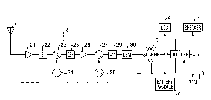
Referring to Figure 1 of the drawings, a radio
pager embodying the present invention is shown and
includes a half-size microstrip antenna 1. A paging
signal (frequency of 930 MHz) coming in through the
microstrip antenna 1 is applied to a radio circuit 2. The
radio circuit 2 receives the paging signal by the double
superheterodyne principle to produce a corresponding
second intermediate frequency (IF) signal (frequency of
455 kHz) and then demodulates it into a digital signal.
The digital signal has its waveform shaped by a waveform
shaping circuit 3 and then fed to a decoder 6. The
decoder 6 compares a call signal included in the digital
signal with an address number assigned to the pager and
stored in a ROM 8. If the former is identical with the
latter, the decoder 6 drives a loudspeaker 5 to produce an
alert tone. At the same time, if the digital signal
includes a message signal, the decoder 6 displays a
message corresponding to the message signal on an LCD 4.
A battery package 7 feeds the radio circuit 2, waveform
shaping circuit 3, and decoder 6. A DC/DC converter, not
9 2069781
shown, is included in the decoder 6 for feeding various
circuits constituting the decoder 6, LCD 4, etc.
The radio circuit 2 includes an amplifier 21 for
amplifying the received signal coming in through the
microstrip antenna 1, a band-pass filter 22, and a first
frequency converter (referred to as a first mixer herein-
after) 23 which receives the output of the band-pass
filter 22. The first mixer 23 mixes the amplified
received signal with a first local oscillation signal
(frequency of 908 MHz and signal level of about -15 dBm)
fed from a first local oscillator 24, thereby outputting a
first IF signal (frequency of 21.4 MHz). The first IF
signal has unwanted high and low frequency components
thereof removed by a band-pass filter 25, amplified by an
amplifier 26, and then applied to a second frequency
converter (referred to as a second mixer hereinafter) 27.
The second mixer 27 mixes the amplified first IF signal
with a second local oscillation signal (frequency of
20.945 kHz) from a second local oscillator 28 to thereby
produce the previously-mentioned second IF signal. The
second IF signal has unwanted high frequency components
thereof removed by a low-pass filter 29 and then converted
to the previously-stated digital signal by a demodulator
(DEM) 30. The receiver further includes a power switch
and other conventional electric and electronic elements,
although not shown or described.
2069781
Referring also to Figures 2, 3 and 4, the radio
pager has a printed circuit board 107 on which electric
and electronic parts 108 implementing part of the receiver
circuitry, i.e., radio circuit 2, waveform shaping circuit
3, loudspeaker 5, decoder 6, and ROM 8 are mounted. Sheet
metal or similar electrical conductive plates 106 and 110
are positioned on both sides of the printed circuit board
107 and LCD 4 supported by the board 107. The conductive
plates 106 and 110 are fastened together by metal screws
103a-103f located around the circuit board 107 and nuts
104a-104f affixed to the inner surface of the conductive
plate 110 by spot welding. An arrangement is made such
that the inner surface of the conductive plate 106 and the
ground surface of the printed circuit board 107 (opposite
to the surface carrying the parts 108) are connected to
each other with respect to DC and high frequency. Hence,
the conductive plates 106 and 110, screws 103a-103f and
nuts 104a-104f form a shield case accommodating the
printed circuit board 107 and electric and electronic
parts 108. This is successful in reducing the radiation
of unnecessary electromagnetic waves from, for example,
the first local oscillator 24 to the outside of the
pager. For example, a radio pager R5N4-14D (available
from NEC Corp., Tokyo, Japan, and on the market since
December, 1991) having the above configuration was found
to reduce the radiation level to 25 ~V at a distance of 3
m without having resort to a shield case for the first
~,
11 2069781
local oscillator 24. The outer surface of the conductive
plate 106 and the earth plate, not shown, of the
microstrip antenna 1 are connected to each other with
respect to high frequency by thermal adhesion with the
intermediary of a thermal adhesion tape 105. With such a
configuration, the pager prevents high-frequency
electromagnetic coupling from occurring between the
antenna 1 and the printed circuit board 107 and parts 108
and insures stable operations of the circuitry mounted on
the circuit board 107. It is to be noted that the
conductive plates 106 and 110 exhibit a satisfactory
electromagnetic shield effect even when locally perforated
or provided with a mesh structure. The screws 103a-103f
and nuts 104a-104f may be replaced with other conductive
connecting pins so long as the pins are capable of
affixing the conductive plates 106 and 110 while spacing
them apart by a predetermined distance.
A frame 102 is implemented as a plastic molding
and surrounds the antenna 1, conductive plates 106 and
110, printed circuit board 107, LCD 4, and battery package
7 to substantially determine the contour of the pager.
Further, a case 101 covers the frame 102, conductive
plates 106 and 110, antenna 1 and other parts constituting
the pager. If desired, smoothly-planed board may be
arranged on the outside of the conductive plates 106 and
110 and antenna 1 to protect the above-mentioned
constituent parts. The conductive plate 110 and case 101
C
12 2069781
(as well as the smoothly-planed board) are provided with
openings to make the display surface of the LCD 4 visible
from the outside of the pager.
As shown in Figures 1 - 4, the conductive plate
106 is bent in a step or crank configuration to form a
recessed flat portion and a projected flat portion. The
earth plate of the microstrip antenna 1 is fitted on the
recessed portion of the conductive plate 106 by pressure
while the battery package 7 having a substantial height is
accommodated in the projected portion of the plate 106.
Specifically, since the conductive plate 106 is far
thinner than the antenna 1, it is bent in a crank
configuration to increase the space available in the pager
by an amount corresponding to the thickness of the antenna
15 1.
The microstrip antenna 1 has an antenna element
11 and receives a paging signal in a direction
perpendicular to the general plane of the antenna element
11, i.e., in the frontal direction of the pager. In the
antenna 1, a short circuit 13 is constituted by a number
of through-holes 13a and forms the short-circuit end of
the antenna element 11. A through-hole 12 is interposed
between the short circuit 13 and the open end lla of the
antenna element 11, defining the feed point of the antenna
1. The previously-mentioned projected portion of the
conductive plate 106 equivalently constitutes an earth
plate of the antenna 1 to thereby increase the overall
~.~
13 2 0 69 781
area of the earth plate and, therefore, the antenna gain
Ga in the frontal direction. A jumper line, e.g.,
soldered wire 109 connects the through-hole 12 and the
input terminal of the radio section 2 (input terminal of
amplifier 21) mounted on the printed circuit board 107.
As shown in Figures 5(a) and 5(b), the
microstrip antenna 1 and conductive plate 106 constitute
an antenna assembly. To fabricate the antenna 1, a
dielectric base plate 15 made of Teflon and carrying
copper foil on both surfaces thereof is etched to remove
part of the copper foil. As a result, the antenna 1 has
the quadrangular antenna element 11 on one surface and a
conductive earth plate 16 on the other surface, the earth
plate 16 extending over substantially the entire area of
the antenna 1. A side conductive plate 14 surrounds the
antenna element 11 on the surface of the base plate 15
where the antenna element 11 is formed. A number of
through-holes 14a are formed on the side conductive plate
14 adjacent to the edges of the latter, whereby the
conductive plate 14 is maintained at the same potential as
the earth plate 16, i.e. ground potential. Further, the
antenna 1 has a land 18 on the surface thereof where the
earth plate 16 is located. The land 18 is connected to
the through-hole 12 and insulated from the earth plate 16,
defining the feed point 17 of the antenna 1.
Assume that the velocity of light is C0, the
dielectric constant of the dielectric base plate 15 is ~r,
.~
-
14 2069781
and the distance between the open end lla of the antenna
element 11 and the short circuit 13 is Dl. Then, a
resonance frequency fO that maximizes the gain Ga of the
microstrip antenna 1 may be expressed as:
fO - CO / { 4D1 (~r) ~}
which is very sensitive and depends upon, for example, the
thickness t of the base plate 15. Assume that the
frequency fO is 930 MHz, and that the base plate 15 is
made of Teflon and has a dielectric constant ~r of 2.17
and a thickness t of 1.6 mm. Then, the distance D1 is
54.5 mm as determined by calculation, although it was
found to be 55.3 mm by actual measurement. The short
circuit 13 and the through-hole 12 are spaced apart by a
distance S which is selected to match the input impedance
of the radio circuit 2 after the impedance of the antenna
1, as viewed from the radio circuit 2 side, has been
determined.
As shown in Figure 5, the through-holes 14a and
side conductive plate 14 surround the screws 103a-103d and
isolate them from the antenna element 11. Therefore,
whatever dimension and whatever position the screws 103a-
103d may have under the above condition, they do not
effect the radiation pattern of the antenna 1 at all.
Specifically, assume that a surface current S41 flows
through the antenna element 11 and earth plate 16, and
`~ `
..,,..~
2069781
that the screws 103a-103d, side conductive plate 14 and
through-holes 14a are absent. Then, the surface current
S41 will turn into a displacement current S42 at the open
end lla of the antenna element 11, and the current S42
will be terminated by the earth plate 16 and again turn
into the current S41. On the other hand, if the side
conductive plate 14 and through holes 14a are absent and
the screws 103a-103d are located in the vicinity of the
antenna element 11, a displacement current, not shown,
from the open end lla will be coupled to the screws 103a-
103d as well. In this manner, the displacement current
S42 is dependent on the dimension and potential of the
screws 103a-103d, so that the radiation pattern of the
antenna 1 is effected by the screws 103a-103d. This makes
it difficult to predict the directivity characteristic of
the antenna 1 at the design stage of a radio pager. In
the illustrative embodiment, since the side conductive
plate 14 and through-holes 14a adjoin the antenna element
11 to be electromagnetically isolate it from the screws
103a-103d, the surface current S41 will by simply split
into a displacement current S43 directed to the side
conductive plate 14 and the displacement current S42
directly terminated by the earth plate 16. Since the side
conductive plate 14 assumes a fixed position and has a
fixed size, the displacement current S42 is not effected
by the dimension and potential of the screws 103a-103d
and, therefore, the radiation pattern of the antenna 1 is
~,
16 2069781
not disturbed by the screws 103a-103d. Clearly, such an
electromagnetic shield effect is achievable despite other
conductive structural parts and elements which may be
included in the pager, so long as such parts and elements
are surrounded by the side conductive plate 14 and
through-holes 14a.
The antenna gain Ga of the microstrip antenna 1
in the frontal direction increases as the area of the
earth plate 16 increases beyond the area of the antenna
element 11, as stated earlier with reference to Figures 2
to 4. In the antenna assembly shown in Figure 5, the
conductive plate 106 is connected to the earth plate 16
with respect to high frequency, and the flat projected
portion of the plate 106 exten~ing in the same direction
as the earth plate 16 is further extended from the short
circuit 13 over a distance W1 to provide the antenna 1
with an extra earth plate area. The antenna assembly,
therefore, has a greater antenna gain Ga in the frontal
direction than with the antenna 1 alone. Specific
numerical values regarding the antenna gain Ga will be
described later.
Figure 6 shows another specific construction of
the antenna assembly. As shown, the antenna assembly is
made up of a microstrip antenna 50 and the conductive
plate 106. The antenna 50, like the antenna 1 of Figure
4, has an antenna element 51 including an open end 51a and
a short circuit 53, a through-hole 52, side guide plates
. ~
17 2069781
54a and 54b, and an earth plate, not shown. The
difference is that the side guide plates 54a and 54b are
separated from each other since there is no side guide
plate that faces the open end 51. The antenna element 51
has the conductor thereof partly removed to form slits 55a
and 55b in the vicinity of the short circuit 53. The
slits 55a and 55b have lengths L1 and L2, respectively.
With the slits 55a and 55b, it is possible to lower the
resonance frequency fO of the antenna 1 and, therefore, to
reduce the size of the antenna 50. Specifically, the
antenna 1 of Figure 5 implements the resonance frequency
of 930 MHz by spacing apart the short circuit 13 and the
open end lla by a distance Dl of 55.3 mm. By contrast, in
the antenna 50 of Figure 6, the slits 55a and 55b are
formed in the antenna element 51 over a length Ll of 7.5
mm and a length L2 of 6 mm, respectively, whereby the
distance D2 between the short circuit 53 and the open end
51a is desirably reduced to 48 mm.
Referring also to Figure 7, the earth plate of
the microstrip antenna 50 has dimensions E and F which are
nearly equal to each other and are substantially 50 mm,
and the conductive plate 106 extends over a distance W2 of
30 mm as measured from the end of the antenna 50. The
antenna assembly was measured to have an antenna gain Ga
in the frontal direction which was about 1.5 dB greater
than the case wherein the distance W2 was zero, i.e.,
wherein the conductive plate 106 was not connected to the
18 2069781
earth plate of the antenna 1 with respect to high
frequency. Obviously, such an increase in antenna gain Ga
is also attainable with the antenna assembly of Figure 5.
Experiments showed that the antenna directivity pattern is
effected little by the step between the outer surface of
the conductive plate 106 and the earth plate of the
antenna 50, which step is equal to the thickness of the
dielectric base plate which is substantially 1.6 mm.
Further, in the embodiment of Figures 2 to 6,
instead of the through-holes 13a (53a), the short circuit
13 (53) may be constituted by through-holes 13b (53b)
which are positioned on the side of the open end lla
(51a). In this case, the case 101 may be constituted by a
metal plate and a frame.
In summary, the radio pager of the present
invention has the two conductive plates 106 and 110 and
screws 103a-103f which constitute a shield case
surrounding the printed circuit board 107 and electric and
electronic parts 108. The shield case reduces the
radiation of unnecessary electromagnetic waves to the
outside of the pager from, for example, the first local
oscillator 24 while stabilizing the operation of the pager
circuitry.
The antenna earth plate 16 is connected to the
crank-shaped conductive plate 106 with respect to high
frequency, and the flat projected portion of the plate 106
equivalently plays the role of an antenna earth plate.
19 2069781
Therefore, the area of the antenna element 11 suffices for
the area of an expensive microstrip base plate alone.
This, coupled with the fact that an extra space for
accommodating parts and corresponding to the thickness of
a microstrip base plate is available, promotes the
miniaturization of a radio pager.
The side conductive plate 14 is provided on the
surface of the antenna where the antenna element 11 is
positioned in such a manner as to surround the antenna
element 11, and it is connected to the earth plate 16 by
the through-holes 14a. Hence, so long as the screws 103a-
103d and other structural parts and elements of the pager
are surrounded by the through-holes 14a, the radiation
directivity pattern of the antenna 1 is not effected at
all by changes in the position and size of the structural
elements and parts. This enhances the structural design
freedom of the pager.
When the slits 55a and 55b are formed in part of
the antenna element 51 of the microstrip antenna 50, the
resonance frequency fO of the antenna 50 and, therefore,
the area of the antenna element 51 can be increased to
thereby implement a miniature radio pager.
Although the invention has been described with
reference to the specific embodiment, this description is
not meant to be construed in a limiting sense. Various
modifications of the disclosed embodiment, as well as
other embodiments of the invention, will become apparent
C
2069781
to persons skilled in the art upon reference to the
description of the invention. It is therefore
contemplated that the appended claims will cover any
modifications or embodiments as fall within the true scope
of the invention.