Note: Descriptions are shown in the official language in which they were submitted.
2069973
AN ALL DIGITAL CONFERENCE CIRCUIT
CROSS-REFERENCE TO RELATED APPLICATIONS
The present application is related to the following
co-pending U.S. patent application both being assigned to
the same assignee, entitled:
"POWER-UP AND INITIALIZATION OF A MULTIPROCESSOR
SYSTEM", "(Attorney Docket 91-1-205)".
FIELD OF THE INVENTION
The present invention relates in general to telecom-
munication systems, and more particularly, to a DigitalMulti-Port Conference Circuit for providing up to twenty-
four party conference call.
BACKGROUND OF THE INVENTION
In order for a conference conversation to be as
natural as possible, a conferee must be able to hear
other conferee's speech at all times. Thus, the confer-
ence circuit should be able to handle periods of inter-
ruptions when two or more people may be talking. To do
this basic conference function, the conference circuit
must add up the signals from all the conferees. Before
the summed signal is sent back to an individual conferee,
this conferee's voice sample must be subtracted from the
sum so that the conferee does not hear his own voice.
The conference circuit also must take care of reflected
2S energy and unwanted noise.
Prior to the present invention, CODECs (Coder-
Decoder) and analog OP-AMPs were used to create a pseudo
digital conference circuit. The conferees' voices were
presented to the conference card in the form of a PCM
(Pulse Code Modulation) bit stream. The prior conference
circuit used CODECs to extract samples from this bit
stream and convert them into analog form. The analog
output of up to ~ CODECs was then fed into OP-AMPS, which
did the summation necessary for a conference circuit.
The output of the summation OP-AMPs were fed back into
.: , : : .
:. ,,, : :
" . ,~ , . . . .
2069973
the CODECs to be reconverted to digital PCM information.
The resulting digital information was then placed into
the PCN digital stream by the CODEC.
One of the fundamental limitations of the old con-
ference card was its inadequate handling of energy re-
flected from the hybrids. When a conference circuit
sends a signal toward one of the conferees the signal
interacts with the conferee's hybrid that does the 4 wire
to 2 wire conversion. This conversion is not perfect and
some of the energy is reflected back toward the confer-
ence circuit. If this reflected energy is not accounted
for by the conference circuit, the quality of the confer-
ence call can be severely degraded.
In the new circuit, digital echo cancellation is
used to remove the unwanted reflected echo. Echo cancel-
lation is a technique that uses digital signal processing
to synthesize a replica of the echo, which is subtracted
from the conferee's signal. Once the echo is subtracted,
only the desired signal remains. The details of digital
echo cancellation are beyond the scope of this document
and will not be discussed further. For more information
see, e. g., David Messerschmitt et. al., Digital Voice
Echo Canceller with a TMS32020, in Digital Signal Pro-
cessing Application with the TNS320 Family Theory, Algo-
rithms, and Implementations (Texas Instruments 1~86)
(incorporated herein by reference).
It is therefore a primary objective to provide an
all digital solution to conference calling circuits.
SUMMARY OF THE INVENTION
In order to accomplish the object of the present in-
vention there is provided a digital conference circuit
for creating a conference call. The digital conference
circuit receives a received Pulse Code Modulated (PCM)
bit stream and transmits a transmitted PCM bit stream.
Both the received PCM bit stream and the transmitted PCM
bit stream contain a plurality of digital voice samples
where each of the plurality of digital voice samples
--2--
: ~ . , i, . . .
., ' " ;" '.. ; ' : :'
2069973
digitally represents an individual party of the confer-
ence call.
The digital conference circuit includes a time slot
assigner that determines an appropriate time to extract
from the received PCM bit stream and to inject into the
transmitted PCM bit stream.
There are a plurality of CHANNEL DSP that extract
the plurality of digital voice samples from the received
PCM data stream, where each of the plurality of CHANNEL
DSP extracts from the plurality of digital voice samples
one unique digital voice sample that represents an indi-
vidual party to the conference call. After extracting
the plurality of digital voice samples, the plurality of
CHANNEL DSP converts the samples from a logarithmic for-
mat to a linear format. The plurality of CHANNEL DSP
next removes any echo from the linear voice samples.
Next, a CONFERENCE DSP receives the linear voice
samples from the plurality of CHANNEL DSP and determines
their sum. The plurality of CHANNEL DSP subtracts from
the sum the digital voice sample that represents the
unique individual party, to create a plurality of indi-
vidual conference sum samples.
Finally, the plurality of CHANNEL DSP convert the
individual conference sum samples to a logarithmic for-
mat. The plurality of CHANNEL DSP then injects the
logarithmic voice samples into the transmitted PCM data
stream.
DESCRIPTION OF THE DRAWINGS
A better understanding of the invention may be had
from the consideration of the following detailed descrip-
tion taken in conjunction with the accompanying drawings,
in which:
FIG. 1 shows a block diagram of the present
invention.
FIG. 2 is a timing and operation diagram for the
CHANNEL DSPs.
FIG. 3 is a timing and operation diagram for the
CONFERENCE DSPs.
- - . . : :
. . , ~: ~ ~: -: . :, ::: : . . :,
. ::- . ~ . ,. .: . . - . .
2~69973
FIG. 4 shows the cabling arrangement for two and
three DMPCC cards.
DESCRIPTION OF THE PREFERRED EMBODIMENT
The Digital Multi-Port Conference Circuit (DMPCC) is
intended to provide up to twenty-four conferees with con-
ference capability. The construction of the Digital
Multi-Port Conference Circuit (DMPCC) is in such a way as
to allow for the interconnection of up to three DMPCC
cards; thereby, providing for bridge sizes of eight, six-
teen or twenty-four ports.
OVERALL ARCHITECT
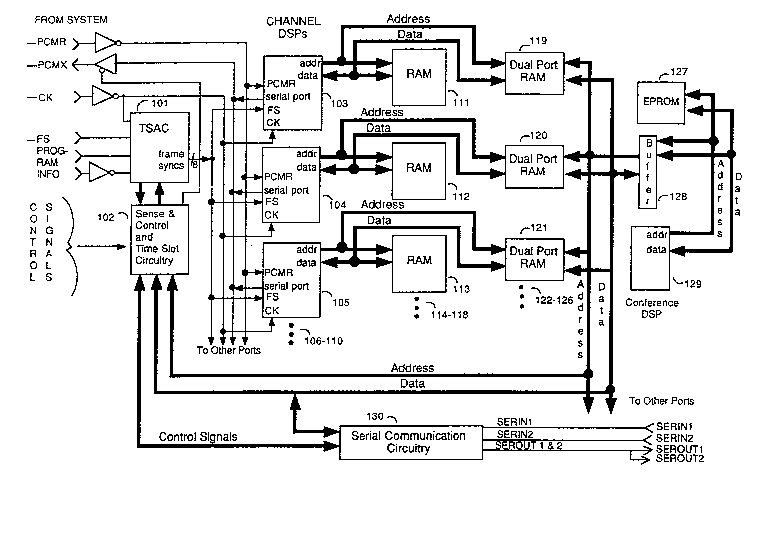
Referring first to FIG. 1, the block level diagram
will now be described. The DMPCC uses Digital Signal
Processors (DSP) to implement echo-cancelation on each
line, and also to sum the conference samples. Specifi-
cally, the DSP chip used in the present embodiment is the
Texas Instruments TMS320C25. However, any of the general
purpose DSPs on the market today could be used with only
slight modification to the present embodiment.
In the DMPCC card, a DSP terminates each channel (or
subscriber) in a manner similar to a CODEC. The DSPs
103-110 each terminate a single line and will be referred
to collecti~ely and individually as CHANNEL DSPs. (Note:
In FIG. 1 only the first three CHANNEL DSPs (103-1~5) and
their associated circuitry are shown.) The CHANNEL DSPs
103-110 perform ~Law to linear conversion, echo-
cancelation, and removal of the subscribers own voice
sample. DSP 129, which is connected to the EPROM 127 and
the other DMPCC cards, performs the summation function
and will be referred to as the CONFERENCE DSP. The
CONFERENCE DSP 129 performs the conference summation of
all local active CHANNEL DSPs and any remote DMPCC
samples.
At a high level, the DMPCC performs the following
events. The CHANNEL DSPs receive the PCM voice samples,
perform echo-cancelation and then send the resultant data
to the CONF~RENCE DSP. Here all channel data samples are
summed and the overall sum is sent back to the CHANNEL
.,
' ' . . ~ ' ~, : . ` . . `
- . - . , ~ :
: . :
20~9973
DSPs. The CHANNEL DSP receives the sum, subtracts the
original data from the sum and transmits the data back
into the PCM data stream.
Using a DSP chip to terminate each channel as stated
above, the CHANNEL DSPs must interface to the PCM bit
stream in a manner similar to the CODECs. The CODECs
communicated with the receive and transmit PCM highways
via two serial ports. Using the ~Law PCM CODEC specifi-
cation as a reference, the serial interface pins on the
CODEC are:
PCMR - Receive PCM highway (serial bus)
interface. At the proper time as
defined by FSR and CLKR, the CODEC
serially receives a PCM byte (8 bits)
through this lead.
CLKR - Master receive clock defines the bit
rate on the receive PCM highway.
FSR - Frame synchronization pulse for the
receive PCM highway.
PCMX - Transmit PCM highway (serial bus)
interface. At the proper time as
defined by FSX and CLKX an 8-bit PCM
byte is serially sent out on this pin.
CLKX - Master transmit clock defining the
bit rate on the transmit PCM highway.
FSX - Frame synchronization pulse for the
transmit PCM highway.
NOTE: In this design CLKR = CLKX = CK; and
FSR = FSX = FS. However, this is not a
requirement and is not meant to limit
the present invention to such a
configuration.
The CHANNEL DSPs 103-110 do not receive time slot
programming information directly from the system. In-
stead, a time slot assigner (TSA) 101 circuitry is used
to receive the programming information. This TSA cir-
cuitry is used to generate one frame sync per channel.
Thus, the CHANNEL DSPs 103-110 will interact with the PCM
highway immediately after receiving a frame sync from the
-5-
- . -
': . ~ : :, . ' : .
. .
!` `' . : .
2~69973
TSA 101 circuitry and do not use an internal timer as the
CODECS did. There will, therefore, be up to nine "frame
sync" type signals, one external frame sync from the
system signifying the start of a frame and, up to eight
frame syncs generated by the TSA circuitry 101 used to
notify the DSPs to shift in the next eight bit sample.
Throughout this document, the former will be referred to
as a system frame sync, the latter will be referred to as
local frame syncs.
In the DMPCC card there is only one EPROM 129, which
is addressed directly by the CONFERENCE DSP 129. The
DMPCC card is designed in this manner for primarily three
reasons: 1) By having only one section of EPROM, future
enhancements or changes are much easier; 2) Firmware
modifications are more economical, and; 3) Because each
CHANNEL DSP does not require its own EPROM, board space
and cost are reduced.
Each CHANNEL DSP has its own associated local RAM:
for example, CHANNEL DSP 103 uses RAM 111 and so on.
This local RAM can be used for either CODE or DATA stor-
age. Because the CHANNEL DSPs do not have their own
EPROM, the CONFERENCE DSP 129, in conjunction with the
CHANNEL DSPs, is responsible for downloading the CHANNEL
RAMs 111-118 with the necessary program code. The DMPCC
card is designed so that when power is applied to the
circuit, the CONFERENCE DSP chip 129 is initialized
first. Specifically, the CONFERENCE DSP chip 129 is
reset and then reads the EPROM 127. Next, the CONFERENCE
DSP 129 does any necessary self-test functions. Once the
CONFERENCE DSP is finished its initialization and self-
test, it reads channel boot program code from the EPROM
127 and writes it into the DUAL-PORT RAMs 119-126, of
each CHANNEL DSP.
While the CONFERENCE DSP 129 is downloading the
DUAL-PORT RAM with the boot program, the CHANNEL DSPs
103-110 are prevented from accessing memory through some
channel initialization circuitry. Once all DUAL-PORT
RAMs are loaded, the CHANNEL DSPs are reset; thereby,
entering their initialization and self-test modules.
- ~ - ., ;
., : . ,.;. , . .: . . . ~
. .
.
-
2~9973
After the CHANNEL DSPs have completed their initializa-
tion and self-test modules, the reminder of the channel
program code is passed from the EPROM 127 to the DUAL-
PORT RAMs by the CONFERENCE DSP 129 and then from the
DUAL-PORT RAM to the CHANNEL RAM by the individual
CHANNEL DSPs. The downloading and initialization of the
CHANNEL DSPs is described in more detail in co-
application: I'POWER-UP AND INITIALIZATION OF A
MULTIPROCESSOR SYSTEM", "(Attorney Docket 91-1-205)".
OPERATION
In order to explain how the DMPCC card functions
during a conference call, the processing of one set of
voice samples from the time they are received by the
CHANNEL DSPs until the time the conference sum is trans-
mitted out, is discussed in the following sections.
In the DMPCC card, the eight CHANNEL DSPs (103-110
of FIG. 1) are performing signal processing on their
respective voice samples using identical firmware. Be-
cause the CHANNEL DSPs are running identical firmware, it
is feasible and desirable to have the CHANNEL DSPs oper-
ate on their respective voice sample simultaneously.
Referring to FIGs. 2 and 3. Consider a snapshot of
four frames in time; frames n, n-l, n-2, and n-3 where
frame n is the current frame. During a frame, frame n
voice samples are being shifted-into the receive serial
port of the CHANNEL DSP, frame n-l voice samples are
being processed by the CHANNEL DSPS, frame n-2 samples
are being summed by the CONFERENCE DSP and the conference
sum derived from frames n-3 samples are being transmitted
out of the CHANNEL DSP transmit serial port (refer to
FIG. 2).
While the serial port is receiving a sample from
frame n and transmitting a sample from frame n-3, the
CHANNEL DSP is processing a sample from frame n-l. 8K
words of memory are provided to the CHANNEL DSP to do the
processing. Near the end of a frame, when the processing
is done, the CHANNEL DSPs write the processed sample to
the bus interface logic (i.e. the DUAL PORT ~AM 119-126
-7
2069973
in FIG. 1) for the CONFERENCE DSP to read upon receiving
a system frame pulse.
After the CONFERENCE DSP has read in the voice
samples from up to eight channels on the card, it then
calculates a sum. The CONFERENCE DSP also adds in any
sums from up to two other cards (up to three cards can be
hooked together to form a conference of up to twenty-
four). For the purpose of explanation, it is assumed
that three cards are hooked together. The DMPCC there-
lo fore needs to do two things; the sum that has been formed
must be sent to the two other cards, and the sum from
each of the two other cards must be read and added to its
own local sum.
Serial communication between the cards is accom-
plished over a 50 ohm coaxial cable. Specifically, in a
three card arrangement, each card will have four cables
connected to it, two cables for transmitting data to the
two other cards and two cables for receiving data. See
FIG. 4 for a diagram of the cabling arrangement.
CHANNEL DSPs
Upon receiving a local frame sync from the TSA cir-
cuitry each active CHANNEL DSP will shift-in the next
eight bits from the PCMR highway into its serial port re-
ceive register. The actual time a sample is read-in de-
pends on the channel assigned to that DSP within a frame.
There can be up to any number of channels in a frame,
however 24 or 32 channels in a frame are the most common
numbers. The present design uses a frame of 24 channels,
however one of ordinary skilled in the art can modify the
present invention to function in a 32 channel frame
system. Voice samples can be shifted-in at the start of
any of the channels. The exact channel these voice sam-
ples will be shifted-in defined by the local frame sync
signal as described supra. The channel number for each
local frame sync is programmed into the TSA (101 in FIG.
1) by the system. When the system frame sync occurs at
the beginning of the next frame, the CHANNEL DSPs begin
processing the new samples.
8--
,'
' ' , ' ' ". ~ ' ' ~j' '''' '' ,
2069973
As stated supra, there are six timing phases in the
CHANNEL DSP which cover a total period of three frames
(375 ~sec). This corresponds to the time when the voice
sample is first read off the PCM receive (PCMR) bus until
the summed conference sample is put on the PCM transmit
(PCNX) bus. The six CHANNEL DSP timing phases are de-
scribed below (Refer to^ FIG. 2, where the individual
phases are represented by the circled phase number.
Phase-l corresponds to the voice samples being
shifted-into the DSP's serial port receive register from
the PCMR bus. Upon receiving the last bit, an interrupt
internal to the DSP is generated to inform the CHANNEL
DSP's firmware that a sample has been received. These
samples are referred to as frame n samples, in FIG. 2,
because they occur in the first frame of the three frame
operation. The samples are not processed until the fol-
lowing frame, in order to allow all CHANNEL DSPs to begin
processing the channel samples in sync.
During phase-2 the CHANNEL DSP reads the voice
sample from the DSP serial port receive register. (These
samples are referred to as frame n-l samples because they
correspond to the sample shifted-in one frame ago.) The
samples are read in almost immediately after a system
frame sync pulse.
Phase-3 occurs when the CHANNEL DSP has completed
echo cancelling on the n-l sample and has written it to
the interface circuitry. This event should occur around
the 13th/24 (or 18th/32) channel segment.
During phase-4 after the CONFERENCE DSP has written
the frame n-2 voice sample to the interface circuitry,
the sample is read by the CHANNEL DSP, this should occur
around channel segment 20/24 (or 27/32) within the frame.
Once this sample is read, gain adjustment and linear to
~law conversion operations take place as well as subtrac-
tion of the subscribers own voice sample.
Phase-5 corresponds to the frame n-2 voice samples
being written to the internal DSP serial port transmit
registers where t:hey are shifted-out to the PCMX bus in
the next frame. This timing is very critical and corre-
_g_
2~69973
sponds to a time right after channel segment 24 (or 32)
within the frame. An interval timer is used to inform
the CHANNEL DSPs the precise timing for this phase. This
timing has been picked so the channel 24 (or 32) frame
n-l sample is shifted-out before the frame n-2 sample is
loaded. Also, the serial port must be loaded before the
channel 1 frame n-3 sample is shifted-out.
Phase-6 is the last phase and corresponds to frame
4/24 (or 5/32) where the frame n-3 voice samples are
shifted from the DSP serial port transmit registers onto
the PCMX bus. This shifting begins when the local frame
sync pulse is received from the TSA circuitry. Once this
pulse is received, eight bits are serially shifted-out to
the PCMX bus.
CONFERENCE DSPs
There are four phases of timing per frame for the
CONFERENCE DSP. Refer to FIG. 3, where the individual
phases are represented by the circled phase number.
There is a two frame delay from when the voices are
pulled off the PCM receive bus until the CONFERENCE DSP
begins processing these samples. Interrupts and an in-
ternal timer are used to synchronize the timing with the
CHANNEL DSP.
At Phase-l the CONFERENCE DSP reads the frame n-2
samples from the interface circuitry. This phase begins
immediately after a system frame sync pulse is received.
once read, the sum is calculated for the eight channels.
During Phase-2 the frame n-2 summed voice samples
are written to the two other conference cards. This
should correspond to the channel 3/24 (or 4/32) segment
within the frame.
Phase-3 corresponds to the frame n-2 voice summed
samples being received from the other two conference
cards. These samples are only read if the boards are
present, which is established at the beginning of the
conference call. The timing for this phase is estab-
lished by the internal timer in the CONFERENCE DSP and
is set to match the time when the hardware shifting of
the other two conference samples is complete. Phase-3
--10--
, , - , . , -
.,: , , , . ~ ~ :
2069973
should occur around c~lannel segment 6/24 ~or 8/32). Once
these samples are read they are summed with the previous
sum to form the twenty-four channel conference sum. The
sum is then checked to see if clipping is needed and ad-
justed as necessary.
Phase-4 is the final CONFERENCE DSP phase and corre-
sponds to the conference sum, from up to twenty-four
channels, being written to the eight interface circuits
where they are read by the CHANNEL DSPs. This occurs im-
mediately after phase-3 is completed. The CONFERENCE DSP
then idles until the next frame begins.
After studying FIG. 2 and FIG. 3, it is evident
that during a given frame, several functions are occur-
ring in parallel. To summarize, the parallel processing
can be broken down into three main functions: the serial
port operation, the voice sample processing by the
CHANNEL DSPs and the conference function of the
CONFERENCE DSP.
Although the preferred embodiment of the invention
has been illustrated, and that form described, it is
readily apparent to those skilled in the art that various
modifications may be made therein without departing from
the spirit of the invention or from the scope of the
appended claims.
--11--