Note: Descriptions are shown in the official language in which they were submitted.
20'~0~41
1
LIQUID CRYSTAL COMPOSITION, LIQUID CRYSTAL ELEMENT AND
PROCESS FOR THE PREPARATION OF LIQUID CRYSTAL ELEMENT
S FIELD OF THE IN .NTTnN
The present invention relates to a liquid crystal
composition, a liquid crystal element comprising the liquid
crystal composition and a process for the preparation of the
liquid crystal element.
Display devices utilizing liquid crystal compounds which
are widely employed at present are usually driven by TN
(twisted nematic) mode.
1S When the display device is driven by TN mode, however,
the positions of liquid crystal compound molecules in the
element of the device must be changed in order to change a
displayed image. As a result, there are involvedlsuch
problems that the driving time of the device becomes
2 0 prolonged, and a voltage required for changing the positions
of the liquid crystal compound molecules, namely, power
consumption becomes large.
Switching elements using ferroelectric liquid crystal
compounds, different from those in which TN mode or STN mode
2 S is utilized, are able to function only by changing the
2 .20'0541
molecular orientation direction of the liquid crystal
compounds, and hence the switching time is markedly
shortened. Further, the value of Ps x E, which is obtained
from a spontaneous polarization (Ps) of the ferroelectric
liquid crystal compound and an intensity of the electric
field (E), is an effective energy output for changing the
molecular orientation direction of the liquid crystal
compounds, and accordingly the power consumption is also
significantly diminished. Such ferroelectric liquid crystal
compounds as mentioned above have two stable states, namely,
bistability, in accordance with the direction of the applied
electric field, and therefore show significantly excellent
switching threshold value characteristics. Accordingly, the
ferroelectric liquid crystal compounds are particularly
suitable for display devices for animations.
Antiferroelectric liquid crystals also have the above-
mentioned excellent characteristics, and in addition, they
show easy realization of memory and high contrast.
Accordingly, the antiferroelectric liquid crystals are also
2 0 particularly suitable for display devices.
As the antiferroelectric liquid crystals (also referred
to as "AFLC" for short hereinafter), there have been so far
reported a liquid crystal MHPOBC (abbreviation for [4-(1-
methylheptyloxycarbonylphenyl)4'-octyloxybiphenyl-4-
2 5 carboxylate], etc.
3 _207041
However, the conventionally known antiferroelectric
liquid crystals are insufficient in the orientation
characteristics when practically used for display devices.
For enhancing the orientation characteristics of the
aforementioned ferroelectric liquid crystal, molecules of the
ferroelectric liquid crystal are arranged in such a manner
that the liquid crystal is in a cholesteric phase on the high
temperature side where the molecules can be freely
orientated, and that the liquid crystal phase is changed to
be Iso (liquid phase) - Ch (cholesteric phase) - SmC* (chiral
smectic phase) as the temperature is changed from a high
temperature to a low temperature to make the initial
orientation directions of the molecules almost the same. As
a result, high orientation of the ferroelectric liquid
crystal molecules can be achieved.
As for the antiferroelectric liquid crystals (AFLC),
however, no liquid crystal showing phase change of Iso - Ch -
(SmA) - SmCA* (AFLC phase) in accordance with lowering of a
temperature has been found yet.
An object of the present invention is to provide a
liquid crystal composition capable of producing display
devices having excellent characteristics such as high
2 5 orientation characteristics of a liquid crystal contained
4 _ ~o7o~m
therein, easy orientation of the liquid crystal, an
especially wide operating temperature range, a high switching
speed, an appropriate switching threshold voltage, an
extremely small amount of power consumption, and a high
contrast.
Another object of the present invention is to provide a
liquid crystal element comprising the above-mentioned liquid
crystal composition and a process for the preparation of the
liquid crystal element.
The liquid crystal composition of the present invention
comprises at least one kind of a compound which shows an
antiferroelectric phase and at least one kind of a compound
which shows a cholesteric phase.
In the liquid crystal composition, a carboxylic acid
ester compound represented by the following formula [A] is
preferably contained as the compound which shows an
antiferroelectric phase.
II ~ XlYlZl
Ri-Bi-Ai-Bz-A2-Bs-As-C-0-Ba- i * -~ CHz ~ B5-R2
H ... [A]
In the formula [A], R1 is an alkyl group of 3-20 carbon
atoms or a halogenated alkyl group of 3-20 carbon atoms; B1,
20'~0~41
B2, B3 and BS are each independently a group selected from the
group consisting of -O-, -COO-, -OCO-, -CHz-CHZ-, -CH=CH-, -
CHZO-, -OCHZ-, -S-S-, -S-, -CO-CH2-, -CHZ-CO-, -NH-CO-, -CO-
NH-, -CH=N-, -N=CH-, -NH-, -CO-, -NH-NH-, -NH-CHZ- and -CHZ-
S NH-, or a single bond; B9 is -(CHz)W- wherein w is an integer
of 0 to 3; Al, A2 and A3 are each independently a group
selected from the group consisting of
~~- ~ o H
-~-, H o , 0 0
H H
N ,
N , i i
F and
F
or a single bond and A1, A2 and A3 may be substituted by a
halogen such as fluorine and chlorine or a lower alkyl group
such as methyl or ethyl; X1, Y1 and Z1 are each independently
a hydrogen atom or a halogen atom; n is an integer of 0 to 4;
and R2 is an alkyl group of 1-20 carbon atoms.
_ 20'~054i
6
In the liquid crystal composition, a compound
represented by the following formula [B] is preferably
contained as the compound which shows a cholesteric phase.
CH3
S Rg-B6-Aq-B~~Bg-A5-B9-f- CH2~ C*H-Rq . . . [B]
In the formula [B], R3 is an alkyl group of 3-20 carbon
atoms or a halogenated alkyl group of 3-20 carbon atoms; B6 is
-O- or a single bond; B~, Be and B9 are each independently -
COO-, -OCO- or a single bond; Aq and A5 are each independently
a group selected from the group consisting of
~~ and
or a single bond; m is an integer of 1 to 3; and R4 is an
1$ alkyl group of 2-5 carbon atoms.
By the use of the liquid crystal composition of the
invention, there can be obtained display devices having
excellent characteristics such as high orientation
characteristics of the liquid crystal contained therein, easy
2 0 orientation of the liquid crystal, an especially wide
operating temperature range, a high switching speed, an
2070541
appropriate switching threshold voltage, an extremely small
amount of power consumption, and a high contrast.
Fig. 1 is a diagram schematically showing one embodiment
of the liquid crystal element according to the invention.
Fig. 2 is a diagram schematically showing another
embodiment of the liquid crystal element according to the
invention.
The liquid crystal composition of the present invention
and uses of the composition are described below in detail.
In the liquid crystal composition of the invention, at
least one kind of a compound in an antiferroelectric phase
and at least one kind of a compound in a cholesteric phase
are contained.
As the liquid crystal (compound) in an antiferroelectric
phase, there are, for example, the aforementioned MHPOBC
2 0 compound, a carboxylic acid ester compound represented by the
following formula [A] and compounds represented by the
following formulas:
F
C8H1~0 ~~ COO O COO-C*H (CF3) -C6H13
2d7d~41
s
COO COO ~ COO - C*H (CF3) -C6Hls
CioHzl
In the liquid crystal composition, it is preferred that
at least one kind of a carboxylic acid ester compound
represented by the following formula [A] is contained as the
antiferroelectric liquid crystal. The carboxylic acid ester
compound represented by the formula [A] is also referred to
as "Compound [A]" hereinafter.
RZ-B1-A1-82-A2-83-A3-C-~-89- i * ~ CH2 ~ BS-R2
1 0 H ... [A]
In the formula [A], R1 is an alkyl group of 3-20 carbon
atoms, preferably an alkyl group of 6-16 carbon atoms, or a
halogenated alkyl group of 3-20 carbon atoms, preferably a
1 5 halogenated alkyl group of 6-16 carbon atoms.
When R1 in the formula [A] is an alkyl group of 3-20
carbon atoms, the alkyl group may be either a straight-chain
form, a branched form or an alicyclic form. A carboxylic
acid ester molecule with R1 of a straight-chain alkyl group,
2 0 however, exhibits excellent liquid crystal properties due to
the linearly extended rigid straight structure of the
molecule. Concrete examples of the straight-chain alkyl
20'0541
9
group include hexyl, heptyl, octyl, nonyl, decyl, undecyl,
dodecyl, tetradecyl, hexadecyl and octadecyl.
When R1 is a halogenated alkyl group of 3-20 carbon
atoms, an example of such halogenated alkyl group is a group
S obtained by substituting at least a part of hydrogen atoms of
the above-mentioned alkyl group with halogen atoms such as F,
C1, Br and I.
B1, B2, B3 and BS are each independently a group selected
from the group consisting of -O-, -COO-, -OCO-, -CHZ-CH2-, -
1 O CH=CH-, -CH20-, -OCH2-, -S-S-, -S-, -CO-CH2-, -CH2-CO-, -NH-
CO-, -CO-NH-, -CH=N-, -N=CH-, -NH-, -CO-, -NH-NH-, -NH-CHZ-
and -CH2-NH-, or a single bond. Of these, each of B1 and BS
preferably is any of
-O-, -COO-,
-OCO-,
-CO- and
a single
bon, and each of B2 and B3 preferably is of -O-, -COO-,
any -
15 OCO-, -CH2-CHZ-, -OCHZ- and a singlebond. More
-CHZO-,
preferably, B1 is -O- a single bond, eachof BZ and B3 is
or
any of -COO-, -OCO- and -CH2-CH2-, and BS -COO-, -OCO- or
is a
single bond. When each of B1, B2, B3 and is such a group
BS
as above or a single bond, a liquid crystal composition
2 0 exhibiting high orientation characteristics can be obtained.
B9 is -(CH2)W- (wherein w is an integer of 0 to 3). As
B9, preferred is - (CHZ) - or a single bond (w=0) .
Al, A2 and A3 are each independently a group selected
from the group consisting of
2070541
to
~o, o o, ~o~~-
~ ~-, o o .
,
N ,
-~ o~-- ~ o~- O
N , , ;
F and
F
or a single bond. Of these, preferred are the following
groups and a single bond.
~o-, o o , H o ,
More preferably, A1 and A2 are each independently a group
selected from the group consisting of
20'~0~41
11
~O- , 0 0
O H and H O
and A3 is a group selected from the group consisting of
~o , o o , ~,
00 ,
Especially when A1 is
O H
and each of AZ and A3 is
a liquid crystal composition showing excellent properties
(e. g., high contrast) can be obtained.
2070541
12
These A1, A2 and A3 may be substituted by a halogen
atom such as fluorine and chlorine or a lower alkyl group
such as methyl or ethyl.
X1, Y1 and Z1 are each independently a hydrogen
atom or a halogen atom, and it is preferred in the invention
that all of X1, Y1 and Z1 are hydrogen atoms or all of X1. Y1
and Z1 are halogen atoms.
The symbol n is an integer of 0 to 4, preferable 0
or 1.
R2 is an alkyl group of 1-20 carbon atoms,
preferably an alkyl group of 1-10 carbon atoms.
Particularly preferred among the carboxylic acid
ester compounds of the formula [A] are those in which:
R1 is an alkyl group of 3-20 carbon atoms or a
halogenated alkyl group of 3-20 carbon atoms;
B1 is a single bond or -0-;
B2 is -C00- or -CH2CH2-;
B3 is a single bond, -C00- or -CH2CH2-;
B4 is -(CH2)w- wherein w is an integer of 0;
A1 and A2 are each independently a ring selected
from the group consisting of:
~o , o o .~.
0 0 . ~..~~.
each of which may be substituted by a halogen or a lower
72932-131
20 70 54 1
12a
alkyl group;
provided that at least one of A1 and A is a group
of the formula:
which may be substituted with a halogen atom or a
lower alkyl group;
when B3 is a single bond, A3 is a single bond and
when B3 is -C00- or -CH2CH2-, A3 is
CX1Y1Z1 is methyl or trifluoromethyl;
n is an integer of 0 to 4; and
R2 is an alkyl group of 1-20 carbon atoms.
Specific examples of the carboxylic acid ester
compounds showing antiferroelectricity which are represented
by the formula [A] include compounds described in Unexamined
Japanese Patent Publications No. 1(1989)-226857, No. 2(1990)-
40346, No. 2(1990)-264746 and No. 2(1990)-264747 and
compounds indicated by Compound Nos. [A-1] to [A-55] set
forth in Table 1. The antiferroelectric carboxylic acid
ester compounds also include compounds which are different
from each other only in the length of terminal alkyl chain,
such as the compounds indicated by Compound Nos. [A-5] to
72932-1:31
_~ 20 70 54 ~
12b
[A-11] in Table 1.
The symbols in Table 1 have the same meanings as
defined in the compound [A].
Further, the abbreviations in the symbols A1, A2
and A3 have the following meanings.
72932-131
2070541
13
p-Ph:
Bi-Ph:
S
Ph-Cyh:
Cyh:
1 0 Nap
O H
Tet
H O
Rt a
H O ,
Cyh-Ph:
... ~4 20'0541
v
ro
E
H. . ,5 20'0541
VJ H ..~ tf7 tn tn In M M M M M
CC , ~I rr .-~ .-n 'r
N f..
U
I t" c0 N N N N cD c0
tO c0 c0
I I I I I I I I I I
O O O O O O O O O
O
Y! ?~ w x x x x x x w
N
w
f N
3 O
_ ~ ~ ~ .-I M M O O O O O
U
H
C. .C t t t L ,= L
M 0. 0. 0. C4 O. 0. 0.
U ~ 1 I I I 1 I I I I I
a a a a a a a
N
i I I 1 1
1 I
E' C O O o o O o I I I
V V U U U V U
I I 1 1 I 1 I
.C t S L .C L .C
N 0. 0. 0. 0. G. 0. 0.
~, I I I 1 I I I y.~ ,Nt
a a
a a a a a d
E H E,
I I I 1 I 1 1 I I I
N O O O O O O O O
. _
_
O O
O O O O O O O O
O O
U V V U V
V U V V U
1 I I I I I I I I 1
+~ +~ Y +~ +.~ +~ +a +~ ~
N C7 ~ N C1 N C7 d y.
d N
H E' E' E" H E
E H E F
O O I O I 0 I O I
O
CO
I
~
M N N N N N
0.., N N N N
V (O O O O O O O O O o
O' r
r .r .r .r .-~ rr .--I .~ .-i .-i
N M d' ~ O ~ 00 p O
S-1 '~ '~ ~ "~ ~ .-n ..r .r r
r N
I I
I i i I I i I I
U Z
20'~0~41
H M ~''~ M M M
"~ .r .-~ .-I M ~
N L M
M
M
.r
V
L~ cp c0 O ~O c0 tp t0 c0 c0
N
I I ~ I I
O O O O O O O O O O
x w r.>~x x w w x x w
3
a N
_ x 3 0 0 O O O O O O O O
~ U -
H
H
C r
4 L s t t
U ~ I ' n. a. ca.
a I I I I a I I I
.- c. a
_
.4 I
ro ~ 0 1 ~ I
4 V I I I I " o O O I
1 V U U U
1 I I
N t t ~ L'
~, ~ i~ ~ i~ y,i ~ ~'Z'G' O. LY
d d1 N N I I 1 I 1
E~ E-n E E. H d d d d 4
1 I 1
N O I O I I I I I 1
O O O O O
CC Q O V O
U U O O O O
1 O I U V O O U
U U U
U
I
I
t I
Q, (Z (Z,, ~ ~
+~ z z, G1'.,p~" ~E 1J
~ x
~
H
~r~z
x i I I o
I
I
I ~
'r tn .r .r .-r .r
~ .-r
~
.-.
v
~'
N
..w
.-n
(Y, .-r ~ N N N N N
x
o
L' O O O O O
Q
'~ '~ rr
.-r
Z7
", d' In N C' 00 O
N N N ~
M I I I ~ c~
a a a a ~ ~ ~c
Sa ~ a
N
N
N
I
I
a
~
17
207041
H M M M M M M
v1 .r .r .r M M M M
x 'r "'~ ~'~ .r
N f..
V
1 ~ ~ ~ O O t0 c0 c0 t0 ca
I I I I I I I I I I
O O O O O O O O O O
7C >. w x x r~. w w w x x w
N
3
N
,.., x , 3 0 0 0 0 O O O O O O
I-I ~ U
v
C
O
U
I I I I I I I I i I
N
.>a
H
m
w
I I I I I I I I I I
N t t t L .C L ~ Z
4 O. C, O. C. t = i~
a' I I 1 I I I ~' n' IS, U
a a a a a a a a I I
a .a
G>r
I I I ,
N O O O O O I I
(I7 O O C O O 1 O
U U V V I O O
1 7 I 1 G O U
O O
O O
V U
V U
O
I
1
V
.1.~~
-L~J z z
~ z
~
~
!1
~L
'~
~
~
z
z
z
z
I o p
o I
I
o
0
o
I
x --n
N N
N
N
~
N
M
N
U
O O O
O O
O ,.y
p, .-r
~ rr
O
t0
~'~
.--~
.-n
~y
~
O
N
M C O
In ~
(O
f-1 M
M
M
c'~
M
M
M
~
M
I
I
I
I
I
I
I
E I I
E I
V
z
Q
~
~
~C
,$ 2070541
ch c~ c~ M M c'~ c'~
V1 N .--1~r N .--1 N N ~-y ~ ~ H
N L
V
Oi I 7r c0 cD c0 cD cD ~D t0 N N ~D
I I I I
I I I p O I
U V
O O O O O O O .-~ .-r O
C
N CL G4 GL CL w L~ L4 GL (Y GL
3
H r N
3 0 0 0 0 0 0 0 0 0 0
~ U
V
I I I I I I I I I I
ro
H
I I I I
I I I I I I
t t
>. t t t t t t t L i.
N U 0. 0. 0. 0. 0. 0. 0. 0. V
1 I I I I I I 1 1 1
t ..., ." .., .., a a a ' t
a
a. m m m m o"
I t I I I 1 1 I I I
N O O O O O O O O O O
O O O O O O O O O O
U V U V V U V V V U
1 I 1 I I i I I I I
t t t t t t t
7, ~ ~ ~ a
(~f ~ (d V U U V U V U
1 I I 1 I I 1
z z s t t t t t
0. 0. 0. 0. 0. 0. 0.
I o I o I o I O I
CO
I .--n.r rr rr ,-i ..r ...~ .~ ,H
o ~ N N N N N N N N N N
x
o _
V O O O O o O O O O O
a .~ r. r. r. .~ r. .. ~. ...
---. ~ N n'7 V' In tD r ~.....O O
S-1 ~ ~' ~' ~' ~' d' ~' sT V' t!7
I I I I ~ I i I I
I
Q~. C~.
U Z
20'70541
19
M M M
fn N r1 H r1 ~ l!~
x
N L
V
p.,' Y, c0 c0 ~D N N
I
I I
I I I
O O O O O
C,
~C > w w w x x
N
3
a N
~, 3 0 0 0 .. ...
V
>~
O
U
m
I I I I I
O
r~
,p
ro
H
m I I I I I
w
t
a, t t t t
N U L4 C1, CY O.
1 1 ~ I I
t ... .. a a
0. p0 Cp
N N
I 1 I
N O O O N N
0 0 o x x
U V U V V
1 ~ I
S t t
T ~ t t
V U U 0. 0.
1 1 I ~ I
t t t a a
c>r a. c4
I O I O I
P0
1 H
~
- v N N N N N
x
p _
V O O O O O
Q
N M C tn
("p n t17 117 Ifs In
p, ~ I I I i I
20'70541
Such carboxylic acid ester compounds as described above
can be prepared utilizing known synthetic techniques in
combination.
For example; the carboxylic acid ester compounds can be
5 synthesized through the synthetic route as illustrated below.
In the compound shown in the following synthetic route,
R is an alkyl group of 3-20 carbon atoms or a halogenated
alkyl group of 3-20 carbon atoms. R* is an optical active
group of 4-20 carbon atoms having at least one asymmetric
10 carbon atom. Hydrogen atoms which are bonded to the carbon
atoms of the optical active group may be substituted with
halogen atoms such as F, C1, Br and I, preferably a fluorine
atom. Examples of such optical active groups include
-C*H (CH3) -C6H13, -C*H (CH3) -CSH11, -C*H (CZHS) -CSH11, -C*H (C2H5) -
1 $ C6H13, -C*H (CF3) -C6H13 and -C*H (CF3) -CHZ-COO-C2H5.
_ 20'0541
. , 21
CHZ-O ~ COOH HO~
COOR
I N,N'-dicyclohexylcarbodiimide/methylene chloride
RO 0 O COOH
CHZ-O ~ COO ~ COOR*
HZ/5~Pd-carbon/THF
RO H O COOH ~
HO~ COO ~ COOR*
N,N'-dicyclohexylcarbodiimide/methylene chloride
RO H O COO ~ COO ~ COOR*
That is to say, for example, 6-n-alkoxynaphthalene-2-
carboxylic acid is hydrogenated under application of heat and
pressure in the presence of palladium/carbon catalyst, to
obtain 5,6,7,8-tetrahydro-6-n-alkoxynaphthalene-2-carboxylic
acid.
Separately, 4-hydroxybenzoate which is derived from an
optical active alcohol is caused to react with 4-benzyloxy
benzoic acid in a mixture solvent of 4-N,N-
dimethylaminopyridine and methylene chloride while a N,N'-
dicyclohexylcarbodiimide solution is added dropwise, to
obtain 4-(4'-benzyloxybenzoyloxy)benzoate which is derived
from the optical active alcohol.
200541
22
The resulting 4-(4'-benzyloxybenzoyloxy)benzoate which
is derived from the optical active alcohol is introduced into
a solvent such as tetrahydrofuran, and reduced using hydrogen
gas in the presence of a reduction catalyst such as
S palladium/carbon, to obtain 4-(4'-hydroxybenzoyloxy)benzoate
which is derived from optical active alcohol.
Thus obtained 4-(4'-hydroxybenzoyloxy)benzoate which is
derived from the optical active alcohol is caused to react
with the 5,6,7,8-tetrahydro-6-n-alkoxynaphthalene-2-
carboxylic acid obtained in the above stage in a mixture
solvent of 4-N,N-dimethylaminopyridine and methylene chloride
while a N,N'-dicyclohexylcarbodiimide solution is added
dropwise, to obtain a carboxylic acid ester compound
according to the invention.
The above-mentioned process is given as an example of
processes for preparing antiferroelectric liquid crystals
(carboxylic acid ester compounds [A]) used in the invention,
and it should be construed that a process for preparing the
carboxylic acid ester compounds [A] used in the invention are
2 0 by no means limited to this process.
The carboxylic acid ester compound having the formula
[A] prepared as above are used as an antiferroelectric liquid
crystal compound.
The carboxylic acid ester compound, particularly a
2 5 compound indicated by the above-mentioned Compound No. [A-8],
200541
23
is mixed to a cholesteric liquid crystal compound (described
later), whereby a liquid crystal composition remarkably
enhanced in the liquid crystal properties such as contrast
(i.e., orientation properties) can be obtained.
The liquid crystal composition of the invention contains
at least one kind of a compound which shows a cholesteric
phase (i.e., cholesteric liquid crystal compound), as
described before. That is, in the liquid crystal composition
of the invention, at least one kind of the above-mentioned
antiferroelectric liquid crystal compound and at least one
kind of a cholesteric liquid crystal compound are contained,
so that the composition exhibits phase change of Iso
(isotropic phase) - Ch (cholesteric phase) - (SmA (smectic A
phase)) - SmCA* (antiferroelectric phase, AFLC phase) in
accordance with lowering of a temperature, or is enhanced in
the orientation properties of the liquid crystal.
Moreover, by the use of the liquid crystal composition,
there can be obtained display devices having excellent
characteristics such as high orientation properties of the
2 ~ liquid crystal contained therein, easy orientation of the
liquid crystal, an especially wide operating temperature
range, a high switching speed, an appropriate switching
threshold voltage, an extremely small amount of power
consumption, and a high contrast.
20'~0~41
24
Examples of the cholesteric liquid crystal compounds
include compounds represented by the following formulas
C2H50--(( )rN = N-(( )?-CH2-C*H (CH3) -C2H5
~/0
CSH11 ~~ COO-CHZ-C*H (CH3) -CzHs
CzHs-C*H (CH3) -CHZ-O ~~ CN
and a compound represented by the following formula [B].
Particularly, the compound represented by the formula [B]
(also referred to as "Compound [B]" hereinafter) is
preferably contained in the liquid crystal composition of the
invention.
1 $ Compound [B]
CH3
R3-B6-A9-B7~B8-A5-B9~ CH2~ C*H-Rq . . . [B]
In the formula [B], R3 is an alkyl group of 3-20 carbon
2 0 atoms, preferably an alkyl group of 6-18 carbon atoms, or a
halogenated alkyl group of 3-20 carbon atoms, preferably a
halogenated alkyl group of 6-18 carbon atoms; B6 is -O- or a
2070541
single bond; B7, B$ and B9 are each independently -C00-,
-OCO- or a single bond; A4 and A5 are independently a ring
selected from the group consisting of
~o-. o o .~ oo .
or a single bond; m is an integer of 1 to 3; and R4 is an
alkyl group of 2-5 carbon atoms.
Among the compounds of the formula [B],
particularly preferred are those in which R3 is as defined
above; B6 is -0-; B7 is a single bond; B$ is -C00- or -OCO-;
B9 is -C00-, -0- or a single bond; A4 is a single bond; A5 is
10 the ring defined above; and m and R4 are as defined above.
Specific examples of the compounds [B] are set
forth in Table 2. The abbreviations shown in Table 2 have
the same meanings as those in the compounds [AJ.
,~''t 72932-131
270541
26
N
N
G.
V fr N N N N "
A
M
x 1
V
1
O I I
I O O O
~ V I I
t
~ G. d ~. 4
I A I I
, a .~ z .
_ a
..
x
N
1 I 1 1
V O O O
Cn O U U O
.ta o 0 o v
ro
I I I 1
pp I I I I
I I t I
m
0 0 0 0
r. m
ra N .-~ N
x
x
V o 0
a oo ... ~" -.
b ~, N
a N
o i I I
~ I
oa
w co c~
v z
207041
27
Phase transition temperatures of a particularly
preferred liquid crystal composition containing the
antiferroelectric liquid crystal compound (preferably
Compound [A]) and the cholesteric liquid crystal compound
(preferably Compound [B]) are set forth in Table 3.
In Table 3, phase transition temperatures of Compound
[A] (Compound No. (A-8]) and Compound [B] (Compound No. [B-
1]) are also set forth.
As is apparent from Table 3, in the liquid crystal
composition of the invention, physical properties inherently
belonging to each of Compound [A] and Compound [B] entirely
disappear, and the phase transition temperatures of the
liquid crystal composition are completely different from
those of Compound [A] or Compound (B]. This means that the
liquid crystal composition of the invention is not a mixture
in which Compound [A] and compound [B] in the form of liquid
crystal are simply mixed but a homogeneous mixture. Such
homogeneous mixture can be prepared, for example, by a
process as described in Example 1.
2 0 In the tables given hereinafter, Cry, SmCA*, SmA, Ch and
Iso denote a crystal phase, an antiferroelectric phase, a
smectic A phase, a cholesteric phase and an isotropic liquid,
respectively.
... ~0'~0541
28
Table 3
Phase Transition Temperature
Compound Cry-SmCA* SmCA*-SmA SmCA*-Ch SmA-Iso
$ or or or
Cry-SmA SmA-Ch Ch-Iso
[A-8] 44°C 78°C 94°C
[A-8](l0wt.~)
+ [B-1] ( 90wt . ~) 40°C 69°C 80°C 149°C
1B-11 76°C 89°C 155°C
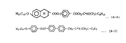
Note: Compound [A-8] and Compound [B-1] are compounds
represented by the following formulas.
HaiCio-O O H COO-(~ COO)2-C*H(CF3)-C6H13
v ... [A-8]
H1~C8-O~OO~~CHZ-C*H (CH3) -C2Hs .
. [B_1 ]
In the case of using the liquid crystal composition of
the invention, there can be obtained liquid crystal elements
2 0 much more improved in the liquid crystal orientation and the
electrooptic response speed, as compared with the case of
using the antiferroelectric liquid crystal alone.
The amount of the antiferroelectric liquid crystal
compound, preferably a liquid crystal compound represented by
29 . 20054.1
the formula [A], contained in the liquid crystal composition
is determined in consideration of properties of the used
compound, viscosity of the composition, operating temperature
range thereof, uses thereof, etc. The amount thereof
generally is in the range of 1 to 99 parts by weight,
preferably 5 to 95 parts by weight, more preferably 15 to 85
parts by weight, per 100 parts by weight of the liquid
crystal composition. When the amount of Compound [A] is
within the above range, the obtained composition maintains
antiferroelectricity and is improved in the orientation
properties. When the amount of Compound [A] is less than 1
part by weight, the obtained composition tends to exhibit no
antiferroelectricity. When the amount thereof exceeds 99
parts by weight, the obtained composition is not improved in
the orientation properties.
The amount of the cholesteric liquid crystal compound
represented by the formula [B] contained in the liquid
crystal composition of the invention generally is in the
range of 1 to 99 parts by weight, preferably 5 to 95 parts by
2 0 weight, more preferably 15 to 85 parts by weight, per 100
parts by weight of the liquid crystal composition. When the
amount of Compound [B] is within the above range, the
obtained composition exhibits antiferroelectricity and is
improved in the orientation properties. Therefore, liquid
2070541
crystal elements comprising the composition show excellent
contrast.
Liquid crystal compositions having antiferroelectricity
such as the liquid crystal composition of the invention show
5 an optical switching phenomenon when an electric field or a
magnetic field is applied thereto as in the case of
ferroelectric liquid crystals. Accordingly, display devices
having a good response can be prepared by utilizing this
phenomenon, as described in Japanese Patent Provisional
10 Publication No. 56(1981)-107216 and No. 59(1984)-118744.
The ferroelectric liquid crystal compounds
conventionally used in the display devices utilizing the
optical switching phenomenon exist in a chiral smectic C
phase, a chiral smectic F phase, a chiral smectic G phase, a
15 chiral smectic H phase, a chiral smectic I phase, a chiral
smectic J phase or a chiral smectic K phase. However,
display elements comprising such liquid crystal compounds
other than those in a chiral smectic C phase (SmC* phase)
generally show a slow response speed. Therefore, driving of
2 0 a liquid crystal element comprising a liquid crystal compound
in a chiral smectic C phase has been considered effective
from the practical standpoint.
The liquid crystal composition of the present invention,
however, can be used not only in an antiferroelectric chiral
2 5 smectic C phase (SmC*A) but also in a smectic A phase by
20'0541
31
utilizing such a method for driving a display device
comprising a liquid crystal material in a smectic A phase as
having been already proposed by the present inventors in
Japanese Patent Provisional Publication No. 64(1989)-3632,
and this is the same as for the ferroelectric liquid crystal
composition which can be used not only in a chiral smectic C
phase (SmC*) but also in a smectic A phase. A method for
driving a liquid crystal element comprising the liquid
crystal composition of the invention will be described later.
The liquid crystal composition of the invention may
further contain other liquid crystal compounds in addition to
the above-mentioned essential components of the
antiferroelectric liquid crystal and the cholesteric liquid
crystal.
Examples of such liquid crystal compounds employable in
combination with the above-mentioned essential components are
as follows.
(+)-4'-(2"-methylbutyloxy)phenyl-6-octyloxynaphthalene-
2-carboxylate,
2 0 4'-decyloxyphenyl-6-((+)-2"-methylbutyloxy)naphthalene-
2-carboxylate,
Liquid crystal compounds such as
32 2070541
HziCio ~ O O CH=N O COO-CHz-C*H (CH3) -CZHs
HzlCio - O ~~ COO O O - C*H (CH3) - C6H13
N~ /~
H2sCii - O ~N~ O O CHz - C*H (CH3) - CZHs
Schiff base liquid crystal compounds such as
H3C - O ~ CH = N ~ C4H9
Azoxy liquid crystal compounds such as
H3C-O--(( )?-N = N~C9Hg
~/O
Benzoic acid ester liquid crystal compounds such as
HgCq-O~COO~C6H13
and
HlsC~-O~ COO CN
Cyclohexylcarboxylic acid ester liquid crystal compounds
such as
H11C5~COO~CN
2 0 and
33 20'0541
HllCs-~ COO-- 0-C5Hli
Biphenyl liquid crystal compounds such as
HllCs~~ CN
Terphenyl liquid crystal compounds such as
HllCs ~~--~ CN
Cyclohexyl liquid crystal compounds such as
HlsC~~~CN
1 5 and
H11CS~O~ CN
Pyrimidine liquid crystal compounds such as
HlsC~~O ~~ CN
~N
The liquid crystal composition of the invention may also
contain other additives which can be added to the
conventional liquid crystal compositions, such as
2070541
34
electroconductivity-imparting agents and life-extending
agents.
When the liquid crystal composition of the invention is
used for a liquid crystal element which is driven utilizing
S dichroism of dyes, the composition may contain dichroic dyes.
The liquid crystal composition of the invention can be
prepared by mixing the antiferroelectric liquid crystal with
the cholesteric liquid crystal, and if desired, other liquid
crystal compounds and additives can be added.
A liquid crystal element comprising the above-mentioned
liquid crystal composition as a liquid crystal material is
described below.
Fig. 1 and Fig. 2 are sectional diagrams showing
embodiments of the liquid crystal element of the present
invention. The same symbols in those figures indicate the
same part.
The liquid crystal element of the invention basically
2 0 comprises, as shown in Fig 1 as an example, a cell 33
including two substrates 31a, 31b facing each other and
having a gap 34 therebetween, and a liquid crystal material
35 filled in the gap. That is to say, the liquid crystal
element of the invention basically comprises a cell 33
2 S composed of two substrates 31a, 31b (also referred to as
2070541
simply "substrate(s)" so arranged as to form a gap 34
therebetween and a liquid crystal material 35 filled in the
gap 34.
At least one of the substrates 31a, 31b is required to
5 be transparent, and examples of the substrate materials
include glass, transparent plastics (e.g., polycarbonate and
TPX (4-methyl-1-pentene polymer or copolymer)) and amorphous
polyolefins (e.g., copolymer of ethylene and
tetracyclo [4, 4, 0, 125, 1w1°] 3-dodecene) .
10 In the invention, flexible transparent substrates such
as various polymer films can be also employed as the
transparent substrates, in addition to the above-mentioned
glass substrates and plastic substrates.
In the case of using a glass substrate, an undercoat
15 layer (i.e., a layer for preventing permeation of unnecessary
components) comprising silicon oxide, etc. as the major
component may be provided on the surface of the glass
substrate to prevent deterioration of the liquid crystal
material caused by elution of an alkali component of the
2 0 substrate.
The transparent substrate has a thickness of usually
0.01 to 1.2 mm when it is a glass substrate.
On the inner sides of the substrates 31a, 31b (i.e.,
sides facing the liquid crystal material), electrodes 32a,
2 5 32b made of indium tin oxide, etc, are provided. In the
zo7o~41
36
invention, a transparent electrode substrate in which a
transparent electrode is united to the above-mentioned
substrate can be also employed as the substrate.
The transparent electrode can be formed by coating the
transparent substrate surface with, for example, indium oxide
or tin oxide.
The transparent electrode has a thickness of usually 100
to 2,000 A.
In the liquid crystal element of the invention, an
orientation control film (i.e., orientation layer) is
preferably provided on the inner surface side (i.e., side
facing the liquid crystal material) of at least one of the
two substrates. More preferably, the orientation control
film is provided on the inner surface side of each substrate.
In Fig. 1, an embodiment of the liquid crystal element
wherein two orientation control films are provided is shown,
and the orientation control films are indicated by 37a and
37b.
In the invention, the orientation control film is an
2 0 organic or inorganic film such as polyimide, silicon oxide,
polyvinyl alcohol, polyamide, polyester, etc., and
particularly a polyimide film is preferable as the
orientation control film. For example, when one orientation
control film is provided in the element, the orientation
2 5 control film is made of polyimide, and when two orientation
2070541
72932-131
films are provided in the element, at least one of them is
made of polyimide, preferably both of them are made of
polyimide.
Any polymers containing an imide bond can be employed as
S the polyimide for forming the orientation control film, and
such polymers preferably have film-forming ability. Concrete
examples of the polyimide include Upirex-R (trade-mark,
available from Ube Industries, Ltd.), Sunever 130 (trade -
mark. available from Nissan Kagaku Kogyo Co., Ltd.), Optomer
A1-1251, JIA-28 (both: trade-mask, available from Japan
Synthetic Rubber Co., Ltd.), Chelimide 601 (trade-mark,
available from Mitsui Petrochemical Industries, Ltd.) and LX-
1400, HL-1100 (both: trademark, available from Hitachi Kasei
Kogyo Co., Ltd.). However, these examples are given by no
means to restrict the polyimides employable in the invention.
As described above, polyimide is a resin containing as a
host component a polymer having imide bond, but the
orientation control film used in the invention may~contain
other resins than the polyimide or resins containing other
2 0 recurring units than the imide recurring unit, provided that
those resins do not mar properties of the polyimide.
When one of the orientation control films is formed from
other material than polyimide, this orientation control is an
organic material or an inorganic material.
20'0541
38
Examples of the orientation control films formed from
organic materials include films of resins such as polyvinyl
alcohol, polyamideimide, polyester, polycarbonate, polyvinyl
acetal, polyvinyl chloride, polyvinyl acetate, polyamide,
polystyrene, cyloxane polyimide, cellulose resin, melamine
resin, urea resin, acrylic resin and electroconductive
polymer.
Further, the orientation control film may be a cured
film of cyclized rubber type photoresist, phenolic novolac
type photoresist or electron rays-photoresist (e. g.,
polymethyl methacrylate and epoxidized 1,4-polybutadiene).
The orientation control film may be formed from an
inorganic material, and examples of the inorganic materials
for forming the inorganic orientation control film include
1 S SiO, Si02, GeO, A1203, Y205, Zr02, MgF2 and CeF3.
The orientation control film can be formed by various
method depending on the material used. For example, there
can be employed a method of applying the resin as mentioned
above on the inner surface of the substrate (i.e., surface
2 0 facing the liquid crystal material) by spin coating and
heating the coated layer of the resin, a method of bonding a
resin film to the inner surface of the substrate, a method of
coating a photosensitive resin thereon and curing the coated
layer under application of energy rays, and a method of
2 5 depositing an organic material thereon.
200541
39
Further, the orientation control film (orientation
layer) can be also formed by chemical adsorption of an
organosilane coupling agent or a carboxylic acid multinuclear
complex, or it can be formed by deposition of silicon oxide
S through a declined vapor deposition. Otherwise, the
orientation layer can be also formed by coating a polyimide
resin on the transparent electrode and then rubbing the
coated resin in the predetermined direction.
The orientation layer may be so formed as to also have a
function of a spacer which is described later.
Two of the transparent substrates 31a, 31b are arranged
in such a manner that the two transparent electrodes 32a, 32b
provided on the substrates face each other and a gap to be
filled with a liquid crystal material is formed between the
two substrates.
The width of the gap 34 (i.e., distance between the
substrates) is usually in the range of 1 to 10 ~.m, preferably
1 to 5 ~t.m. The gap can be easily formed, for example, by
arranging the two substrates in such a manner that they hold
2 0 a spacer therebetween.
The thickness of the orientation control film is
generally in the range of 0.005 to 0.25 elm, preferably 0.01
t o 0 . 15 ~.Lm .
In the invention, the orientation control film is
2 5 provided on the inner side surface of the substrate as
2~'~0~41
described above, and it is preferred that two of the
orientation control films are arranged in such a manner that
the orientation direction of the liquid crystal material
determined by one orientation control film is almost parallel
5 to the orientation direction of the liquid crystal material
determined by the other orientation control film and that
those directions are the same or opposite to each other.
However, arrangement of the two orientation control films is
by no means limited to this case.
10 The orientation control films 37a, 37b function to
orientate the liquid crystal material. Accordingly, the same
or opposite orientation directions of the liquid crystal
material determined by the two orientation control films are
better than a random arrangement of the direction. Thereby,
15 the liquid crystal material introduced into the cell is
enhanced in the initial orientation properties, and as a
result, a liquid crystal element showing high contrast can be
obtained.
The orientation control film has been preferably
2 0 subjected to an orientation treatment. The term "orientation
treatment" used herein means a treatment for orientating the
liquid crystal molecules in the predetermined direction. For
example, polyimide can be orientated by rubbing it with cloth
in one direction.
20'0541
. 41 _
As described above, the cell used in the invention has a
gap 34 to be filled with the liquid crystal material between
two substrates 31a, 31b which are provided, if desired, with
orientation control films 37a, 37b. The gap 34 can be
formed, for example, by arranging the substrates 31a, 31b
holding a spacer 38 therebetween, as shown in Fig. 2. By the
arrangement of the spacer 38, the gap 34 to be filled with
the liquid crystal material can be formed without fail, and
moreover the liquid crystal material can be prevented from
leaking. The gap 34 can be formed not only by a sidewall
having a specific thickness but also by adding particles
having a specific particle diameter (i.e., internal spacer)
to the liquid crystal material.
As the spacer, there can be employed, for example, a
polyimide type polymer material obtained by patterning a
photosensitive polyimide precursor. By virtue of using such
a spacer as mentioned above, a monodomain is formed by
interfacial effect between the spacer and the liquid crystal
material. An orientation film and a spacer can be integrated
2 0 into one system, for example, by using a concentric spacer or
a comb-like spacer which also acts as an orientation film.
Instead of using such a spacer as mentioned above,
fibers can be added to the liquid crystal material, and
thereby the transparent substrates can be held to form a gap
2 5 having a constant width.
42 _ 2170541
Furthermore, granular particles may also be used in
place of or together with the above-mentioned fibers.
The particles as referred to above include those
composed of melamine resin, urea resin or benzoguanamine
resin having a particle diameter of 1 to 10 N.m, preferably 1
to 5 elm, more preferably 1.6 to 5 ~l.m.
The two transparent substrates so arranged as to form a
gap therebetween using a spacer, etc. are then generally
sealed with a sealing material 36 along their peripheries to
be bonded.
Examples of the sealing material 36 include epoxy resin,
UV curable resin and silicone resin, and they may be modified
with acrylic rubber, silicone rubber, etc.
In the liquid crystal element of the invention, a
variety of thin films such as a photoconductive film, a light
screening film and a light reflecting film can be provided
between the orientation control film and the substrate.
In the liquid crystal element of the invention, a liquid
crystal material, that is, the aforementioned liquid crystal
2 0 composition 35, is filled in the gap 34 of the cell.
The liquid crystal element of the invention is
remarkably improved in its properties such as contrast, and
it can be favorably used, for example, as a surface
stabilized ferroelectric liquid crystal element, a surface
2 5 stabilized antiferroelectric liquid crystal element, a
.. . 43 20'~054~
helically modulated element, an overly scattered element, a
guest-host element, a vertically orientated liquid crystal
element.
In a liquid crystal element containing a liquid crystal
composition exhibiting antiferroelectricity, such as the
liquid crystal element of the invention, the element is
beforehand so arranged as to be in a dark state, and a
triangular wave voltage of low frequency is applied to the
element. Through observation of the liquid crystal element
using a polarization microscope, there is found such a double
hysteresis curve that the amount of the transmitted light
becomes the minimum value (i.e., dark state) when the voltage
is 0 (V/~tm) and it becomes the maximum value (i.e., bright
state) when the applied voltage is +Va (V/~.m) and -Va (V/~.m) .
Therefore, an optional bias voltage Vb (0 < Vb < +Va (V/~.m))
between 0 and +Va (V/~.m) is initially applied to the element,
and then an appropriate pulse wave is piled on the bias
voltage and applied to the element, whereby the amount of a
light transmitted by the liquid crystal element can be
2 0 changed from the bright state to the dark state. By driving
the antiferroelectric liquid crystal element in this manner,
the element can be much more enhanced in the apparent memory
properties as compared with the liquid crystal element
utilizing ferroelectricity.
44 2070541
Among the liquid crystal elements of the invention, a
liquid crystal element filled with the liquid crystal
composition in a chiral smectic C phase can be used as a
storage type liquid crystal display element such as a thermal
write type liquid crystal display element and a laser write
type liquid crystal display element. Using these liquid
crystal elements, various liquid crystal display devices and
electrooptic display devices can be produced.
Furthermore, the liquid crystal elements of the
invention can be also used as optical switching elements such
as optical shutters or liquid crystal printers, piezoelectric
elements and pyroelectric elements. Using these liquid
crystal elements, various liquid crystal display devices and
electrooptic display devices can be produced.
The liquid crystal element of the invention can be
driven, for example, by methods described below.
The liquid crystal composition of the invention is
orientated in parallel to the substrates in the cell
utilizing a control power of the substrates. The cell is
2 0 placed between two polarizing plates, and an external voltage
is applied to the liquid crystal element in the
aforementioned manner. As a result, the orientation vector
of the antiferroelectric liquid crystal composition is
changed, and this change of the orientation vector produces
2 S birefringence of the liquid crystal composition. That is,
20~~541
this method is a display method utilizing polarization of the
two polarizing plates and the birefringence. In this method,
the liquid crystal composition is allowed to produce
antiferroelectricity in the cell and reversed in the electric
5 field between two stable states, to conduct optical
switching.
Moreover, such antiferroelectric liquid crystal material
as mentioned above shows apparent memory effect when a fixed
bias voltage is initially applied to the liquid crystal
10 material and then an appropriate pulse wave is further
applied thereto in addition to the bias voltage.
Accordingly, utilizing this memory effect, the liquid
crystal element can be driven under application of an
optional bias voltage to the element. Further, when a
15 display device is produced using the liquid crystal element,
the obtained display device can be remarkably enhanced in
contrast, and a liquid crystal display such as a displayed
image becomes very sharp. Furthermore, the contrast of the
display device is stable and extremely sharp.
2 ~ In the switching element containing the liquid crystal
composition of the invention, switching operation can be
performed by only altering the orientation direction of the
molecule. In this case, the first term of the electric field
applied to the switching element acts on driving of the
2070541
46
element, and therefore the element can be driven at a low
voltage.
The switching element realizes a high speed response of
not longer than several tens of microseconds, and as a result
significantly shorten the operation time thereof.
Accordingly, a display device (liquid crystal display device)
having a large screen with many scanning lines can be easily
produced by using the liquid crystal element. The display
device can be driven at room temperature or at a temperature
not higher than room temperature, and therefore the device
can be driven without auxiliary means for controlling the
driving temperature.
Furthermore, in the liquid crystal material used for the
liquid crystal element of the invention, the molecules of the
material are inducibly orientated when an electric field is
applied even in a smectic A phase where the molecules are
generally considered not to exhibit tristability. Optical
switching can be conducted by utilizing this property.
A second display method of the liquid crystal
2 ~ composition according to the invention is a method in which
the liquid crystal composition of the invention and a
dichroic dye are used, and which utilizes dichroism of the
dye. In this method, display is achieved by changing the
orientation direction of the ferroelectric or
2 5 antiferroelectric liquid crystal composition to change a
.. , 4~ 207041
light absorption wavelength of the dye. The dye used herein
is usually a dichroic dye, and examples of the dichroic dye
include azo dyes, naphthoquinone dyes, cyanine dyes and
anthraquinone dyes.
$ The liquid crystal composition of the invention can be
also employed in other various display methods conventionally
used than the above-mentioned methods.
The display devices produced using the liquid crystal
composition of the invention can be driven by electric
address display system such as static driving, simple matrix
driving and composite matrix driving, optical address display
system, thermal address display system and electron beam
display system.
1$ Process for Pre ar;ng Liquid Gr"y a1 E m nt
A process for preparing such liquid crystal element as
mentioned above will be described below.
The liquid crystal element of the invention can be
basically prepared by filling a gap of the above-mentioned
2 0 cell with a liquid crystal material containing the above-
mentioned liquid crystal composition.
In detail, the liquid crystal material is usually heated
until it becomes in a molten state, and filled (poured) into
the gap of the cell kept at a reduced pressure while being
2 $ molten. After the liquid crystal material is filled in the
20'0541
gap, the cell is usually sealed. Then, the liquid crystal
material filled in the gap of the cell is subjected to an
initial orientation.
For conducting the initial orientation of the liquid
crystal material, the cell having been sealed as above is
heated until a temperature of the liquid crystal material
filled in the cell becomes not lower than the temperature
where it begins to show an isotropic phase, and cooled to a
temperature where the liquid crystal material shows a liquid
crystal phase. In this cooling, the cooling rate is
preferably not more than 2 °C/min, more preferably in the
range of 0.1 to 2.0 °C/min, most preferably in the range of
0.1 to 0.5 °C/min. When the cell is cooled at such a cooling
rate as mentioned above, the liquid crystal material is
improved in the initial orientation, and hence there can be
obtained a liquid crystal element having a liquid crystal
phase free from orientation defects and composed of a
monodomain. The term "initial orientation" designates an
arranged state of a liquid crystal material before changing
2 0 the orientation vector of the liquid crystal material by
applying an electric voltage, etc. to the liquid crystal
element.
The liquid crystal material filled in the gap of the
liquid crystal cell can be orientated, for example, by a
2 S temperature gradient method using a spacer edge or a
20'~0~541
49
monoaxial orientation control method such as a surface
treatment with an orientation film. In the present
invention, the initial orientation of the liquid crystal
material can be also conducted by applying an electric field
formed as the result of applying a direct current bias
voltage to the liquid crystal material while the crystal
material is heated.
By virtue of using the liquid crystal composition of the
invention which comprises both the antiferroelectric liquid
crystal and the cholesteric liquid crystal as described
above, there can be obtained a liquid crystal element having
high orientation properties (high contrast).
Further, in a liquid crystal display device produced
using the liquid crystal element, an operation time can be
markedly shortened, a power consumption can be reduced, and a
stable contrast can be obtained. Moreover, driving at a low
voltage is possible.
2 0 The devices produced using the liquid crystal
composition of the invention utilize antiferroelectric
properties, so that they can be favorably employed for
optical switching system driven at room temperature or a
temperature not higher than room temperature. Further, a
2 S liquid crystal element comprising the liquid crystal
2070541
so
composition is excellent in the memory properties and can be
easily prepared. The liquid crystal composition of the
invention can be remarkably enhanced in the orientation
properties as compared with the conventional liquid crystal
compositions.
Examples of the present invention are given below, but
the invention is in no way limited to the examples.
In the examples, R and S mean an R structure of optical
isomer and a S structure of optical isomer, respectively.
At first, synthesis examples of the antiferroelectric
liquid crystal compounds are given below.
Synthesis of R-1"'trifluoromethylheptyl 4-[4'-
(5",6",7",8"-tetrahydro-6"-n-decyloxy-2"-
naphthoyloxy)benzoyloxy]benzoate
328 mg (1.0 mmol) of 6-n-decyloxynaphthalene-2-
2 0 carboxylic acid and 0.1 g of 5 ~ palladium/carbon were added
to 10 ml of tetrahydrofuran, and the resulting mixture was
stirred in a hydrogen atmosphere at 120 °C and 25 atm.
The temperature and the pressure of the reaction system
were returned to normal temperature and normal pressure, and
2 5 the reaction mixture was then filtrated with celite (filter
20'0541
51
aid). The filtrate was concentrated to obtain a solid, and
the solid was recrystallized with hexane to obtain 90 mg
(0.27 mmol) of 5,6,7,8-tetrahydro-6-n-decyloxynaphthalene-2-
carboxylic acid as a white solid.
second step
To a mixture of 9.20 g (50 mmol) of R-1-trifluoromethyl
heptanol, 11.40 g (50 mmol) of 4-benzyloxybenzoic acid, 0.61
g (5 mmol) of 4-N,N-dimethylaminopyridine and 100 ml of
methylene chloride was dropwise added 70 ml of a methylene
chloride solution containing 11.33 g (55 mmol) of N,N-
dicyclohexylcarbodiimide at room temperature with stirring
over a period of 2.5 hours.
The resultant mixture was allowed to react at room
temperature for 4 hours.
Then, the reaction mixture was filtered, and the
filtrate was concentrated. The concentrate was separated
using column chromatography to obtain 15.96 g (40.6 mmol) of
R-1'-trifluoromethylhexyl 4-benzyloxybenzoate as a~white
solid.
2 0 Thi__rd Step
Into a mixture of 15.96 g (40.6 mmol) R-1'-
trifluoromethylhexyl 4-benzyloxybenzoate obtained in the
second step, 1.6 g of 5 $ palladium/carbon and 80 g of
tetrahydrofuran was blown hydrogen over a period of 8 hours
2 5 at room temperature and normal pressure with stirring of the
20'~0~41
... 5 2
mixture. The reaction mixture was filtrated with celite
(filter aid), and the filtrate was concentrated to obtain
12.34 g (40.6 mmol) of R-1'-trifluoromethylhexyl 4-
hydroxybenzoate as a white solid.
$ Fourth step
To a mixture of 12.34 g (40.6 mmol) of R-1'-
trifluoromethylhexyl 4-hydroxybenzoate obtained in the third
step, 9.26 g (40.6 mmol) of 4-hydroxybenzylbenzoate, 0.49 g
(4 mmol) of 4-N,N-dimethylaminopyridine and 80 ml of
methylene chloride was dropwise added 50 ml of a methylene
chloride solution containing 9.2 g (44.7 mmol) of N,N-
dicyclohexylcarbodiimide at room temperature with stirring
over a period of 2 hours.
The resultant mixture was allowed to react at room
temperature for 3.5 hours.
Then, the reaction mixture was filtered, and the
filtrate was concentrated. The concentrate was separated
using column chromatography to obtain 19.64 g (38.2 mmol) of
R-1'-trifluoromethylhexyl 4-(4'-benzyloxybenzoyloxy)benzoate
2 0 as a white solid.
Into a mixture of 19.64 g (38.2 mmol) of R-1'-
trifluoromethylhexyl 4-(4'-benzyloxybenzoyloxy)benzoate
obtained in the fourth step, 3.0 g of 5 ~ palladium/carbon
2 5 and 100 g of tetrahydrofuran was blown hydrogen over a period
20'0541
53 -
of 14 hours at room temperature and normal pressure with
stirring of the mixture. The reaction mixture was filtrated
with celite (filter aid), and the filtrate was concentrated
to obtain 6.29 g (38.2 mmol) of R-1'-trifluoromethylhexyl 4-
(4'-hydroxybenzoyloxy)benzoate as a white solid.
Sixth step
To a mixture of 0.332 g (1 .0 mmol) of 5, 6, 7, 8-
tetrahydro-6-n-decyloxynaphthalene-2-carboxylic acid obtained
in the first step, 0.424 g (1.0 mmol) of R-1'-
1~ trifluoromethylhexyl 4-(4'-hydroxybenzoyloxy)benzoate
obtained in the fifth step, 0.012 g (0.1 mmol) of 4-N,N-
dimethylaminopyridine and 25 ml of methylene chloride was
dropwise added 10 ml of a methylene chloride solution
containing 0.247 g (1.2 mmol) of N,N'-
dicyclohexylcarbodiimide at room temperature with stirring
over a period of 2.5 hours. The resultant mixture was
allowed to react at room temperature for 2 hours.
The reaction mixture was filtrated, and the filtrate was
concentrated. The concentrate was separated using column
2 0 chromatography to obtain 0.23 g of a white solid.
The M/e value of FD-mass spectrum on the white solid was
738.
From the results of the analyses, the compound was
identified to be R-1"'trifluoromethylheptyl 4-[4'-
s4 20'70541
(5",6",7",8"-tetrahydro-6"-n-decyloxy-2"-
naphthoyloxy)benzyloxy]benzoate which was the aimed compound.
When the liquid crystal temperature range of the
compound was measured, the compound was in a SmCA* phase
s (antiferroelectric phase) between 79 °C and 64 °C, and it was
in a SmA phase between 64 °C and 47 °C.
Each phase transition temperature was determined based
on DSC measurement and phase observation using a polarization
microscope. Further, whether the compound is ferroelectric
or antiferroelectric was judged based on the phase
observation, hysteresis form of the transmitted light and
selection reflection.
Judgement based on the phase observation was made as
follows.
The crystal element is so arranged that it is in a dark
state using a polarization microscope. To the liquid crystal
element were applied a voltage of +30 V/~im and a voltage of
-30 V/N.m. If the liquid crystal element becomes a~ bright
state in each case, the compound is antiferroelectric.
2 0 Judgement based on the hysteresis form of the
transmitted light was made as follows.
The crystal element is so arranged that it is in a dark
state using a polarization microscope. To the liquid crystal
element is applied a triangular wave between +30 V/~im and -30
2 5 V/E.i.m at 0 . 1 Hz or 0 . O1 Hz, and the amount of a light
ss 207041
transmitted by the liquid crystal element is monitored. If
the hysteresis form of the transmitted light is a double
hysteresis form, the compound is antiferroelectric.
Judgement based on the selection reflection was made as
s follows.
The compound is treated with a silane coupling agent to
prepare a homeotropic liquid crystal element. A light is
irradiated onto the liquid crystal element at an incidence
angle of 30°, and a spectrum of the transmitted light is
measured. If the spectrum shows a single trough, the
compound is antiferroelectric.
Synthesis of R-1"-trifluoromethylheptyl 4-(5',6',7',8'-
is tetrahydro-6'-n-decyloxy-2'-naphthoyloxy)benzoate
To a mixture of 0 . 332 g ( 1 . 0 mmol) of 5, 6, 7, 8-
tetrahydro-6-n-decyloxynaphthalene-2-carboxylic acid obtained
in the first step of Synthesis Example 1, 0.304 g ~(1.0 mmol)
of R-1'-trifluoromethylhexyl 4-hydroxybenzoate, 0.012 g (0.1
2 0 mmol) of 4-N,N-dimethylaminopyridine and 25 ml of methylene
chloride was added dropwise 10 ml of a methylene chloride
solution containing 0.247 g (1.2 mmol) of N,N'-
dicyclohexylcarbodiimide at room temperature with stirring
over a period of 1.5 hours. Then, the reaction mixture was
2 s filtrated, and the filtrate was concentrated. The
s 6 20'0541
concentrate was separated using column chromatography, to
obtain 0.30 g of a white solid.
The M/e value of FD-mass spectrum on the white solid was
618.
1H-NMR spectrum on this compound was measured.
From the results of the analyses, the compound was
identified to be R-1"-trifluoromethylheptyl 4-(5',6',7',8'-
tetrahydro-6'-n-decyloxy-2'-naphthoyloxy)benzoate which was
the aimed compound.
Exam, 1
10 ~ by weight of the antiferroelectric liquid crystal
compound [A] represented by Compound No. [A-8] obtained by
the above Synthesis Example 1 or 2 was mixed with 90 ~ by
weight of the cholesteric liquid crystal compound [B]
represented by Compound No. [B-1], to prepare a liquid
crystal composition of the invention.
HaiCio-O 0 H COO-(~ COO)2-C*H(CF3)-C6H13
...[A-8]
H1~C8-O~OO~~CHZ-C*H (CH3) -C2H5
~/ . . [B-1 ]
The phase transition temperatures of the obtained
composition were measured.
200541
s~
The results are set forth in Table 4.
In Table 4, phase transition temperatures of the
compounds represented by Compound No. [A-8] and Compound No.
[B-1] (also referred to simply as "compound [A-8]" and
s "compound [B-1], respectively, and the same can be mentioned
also in other compounds) are also set forth.
Table 4
1 ~ Phas . Trans s s on T ~eratmrP
Compound No. Cry-SmCA* SmCA*-SmA SmCA*-Ch SmA-Iso
or or or
ry-Sm_A A- h Ch-ran
[A-8 ] 4 4°C 78°C 94°C
1 s [A-8] (lOwt.~)
+ [B-1 ] ( 90wt . ~ ) 40°C 69°C 80°C 149°C
fB-11 76°C 8 ° 1 5°C
E. xamnle 2
2 0 The liquid crystal composition obtained in Example 1 was
filled in the cell shown in Fig. 1, to prepare a liquid
crystal element.
The operation temperature range of the obtained liquid
crystal element was between 44 °C and 149 °C, and in this
5g ~0~0~41
temperature range the liquid crystal element showed stable
contrast.
The liquid crystal element was prepared as follows.
The liquid crystal composition set forth in Table 4
(compound [A-8] + compound [B-1]) was melted by heating, and
introduced into the gap kept at a reduced pressure of a cell
which was composed of two transparent substrate having ITO
(Indium Tin Oxide) and two orientation control films (each
thickness: 150 A) each formed on each inner side of the
substrates, as schematically and sectionally shown in Fig. 1,
the orientation control films being made of polyimide
(Optomer AL1251, available from Japan Synthetic Rubber Co.,
Ltd.), and rubbed in such a manner that the orientation
directions become almost parallel to each other and in the
same direction.
After the liquid crystal composition was filled in the
gap of the cell as described above, the cell was heated to
150 °C, held at 150 °C for 5 minutes, and cooled to 60 °C
at
a rate of 1 °C/min, to obtain a liquid crystal element.
2 0 Thus obtained liquid crystal element showed a contrast
of 50.
The cell condition is as follows:
(a) External size: 2.5 cm long x 2.2 cm wide x 1.5 cm
thick
2 5 (b) Substrate: 0.7 mm thick, composed of glass
s9 207041
(c) Distance between substrates: 2 ~m
(d) Sidewall size: 1.8 mm long x 0.1 cm wide x 2 ~Lm
thick
The above-mentioned cell used for evaluation of the
s liquid crystal was prepared in the following manner.
A glass substrate having an ITO transparent electrode
film thereon was coated with polyimide. That is to say, the
ITO transparent electrode film was coated with polyimide
(Optomer AL1251, available from Japan Synthetic Rubber Co.,
Ltd.) by spin coating.
In detail, the polyimide was coated on the electrode
film by means of spin coating method at 2000 r.p.m., and
cured by heating at 180 °C for 1 hour to form a polyimide
film having a thickness of 300 to 400 A. The polyimide film
is was then rubbed with a nylon cloth in one direction, thereby
imparting a liquid crystal orientation ability thereto.
Two of the polyimide film-coated glass substrates
prepared as above were used to form a cell. That ~is, an
epoxy adhesive was applied onto one of the polyimide film-
2 0 coated glass substrates by means of silk screen printing in
order to bond the two substrates together and to control the
gap of the cell. The epoxy adhesive was prepared by mixing
an adhesive base (LCB-304B, available from EHC Co., Ltd.)
with a curing agent (LCB-310B, available from EHC Co., Ltd.)
60 _2070541
and beads (GP-20, available from EHC Co., Ltd.) for
controlling the cell gap in the proportion of 130 . 30 . 3.
The two substrates were stacked in such a manner that
the polyimide films of the substrates faced each other. The
coated epoxy adhesive was cured by stepwise heating at 50°C
for 15 minutes, 60°C for 15 minutes, 70°C for 15 minutes,
80°C for 15 minutes, 125°C for 15 minutes and 170°C for
60
minutes to bond the substrates together.
Using thus prepared cell having a gap of about 2 Etm, the
properties of the liquid crystal were evaluated.
The measurement of contrast in the invention was
conducted as follows. The liquid crystal element was placed
between two polarizers whose polarizing planes met at right
angles, and the liquid crystal element was rotated. The
intensity I of the transmitted light in the bright state and
dark state obtained by the rotation of the liquid crystal
element was measured, and the contrast was determined from a
ratio of I (bright state) / I (dark state) .
2 0 c~~ars son Exampl_~ 1_
The procedure of Example 2 was repeated except for using
only the antiferroelectric liquid crystal compound [A-8] but
not using the cholesteric liquid crystal compound [B-1], to
obtain a liquid crystal element.
2070541
61
The obtained liquid crystal element was evaluated on the
contrast in the above-mentioned manner. As a result, the
contrast of the liquid crystal element was 20.
$ Examples 3 - 6
The procedure of Example 2 was repeated except for
varying the amounts (wt.%) of the antiferroelectric liquid
crystal compound [A-8] and the cholesteric liquid crystal
compound [B-1] to those set forth in Table 5, to obtain
liquid crystal elements.
The obtained liquid crystal elements were evaluated on
the contrast in the above-mentioned manner.
The results are set forth in Table 5.
1 $ Table 5
Compound Phase Transition Temperature (°C) Contrast
[A-8] [8-1] Cry-SmCA* SmCA*-SmA SmCA*-Ch SmA-Iso (60 °C)
(wt.%) (wt.%) or or or
Ex.3 25 75 41 67 145 119
Ex.4 50 50 42 97 146 325
Ex.S 75 25 35 83 136 98
Ex.6 90 10 45 80 1 0 70
2$
- 20'~0~41
62
Examples 7 - 9
The procedure of Example 2 was repeated except for using
the antiferroelectric liquid crystal compound [A-8] in the
amounts set forth in Table 6, and using the cholesteric
liquid crystal compounds [B-2], [B-3] and [B-4] in the
amounts set forth in Table 6 instead of the cholesteric
liquid crystal element [B-1], to obtain liquid crystal
elements.
The obtained liquid crystal elements were evaluated on
the contrast in the above-mentioned manner.
The results are set forth in Table 6.
20'0541
72932-131
_.. 6 3
Table 6
Phase Transition Temperature (°C) Contrast
Compound Cry-SmCA* SmCn*-SmA SmA-Iso
(wt.~) or
C r5r-SmA
Ex.7 [A-8] (26~)
+[B-2] (74~) 62 108 25(70°C)
Ex.B [A-8](25~)
+[B-3] (75~) 36 54 77 19(50°C)
Ex.9 [A-8](24~)
+fB-4] (76$) 41 60 82 21 ( 0° .)
Note: In the above table, the compounds [B-2], [:B-3] and
[B-4] are represented by the following formulas. .
H2iCio-O~O-C0~\~ COO-CHZ-C*H (CH3) -CZHS
. [B_2]
H15C~-O~O-CO-(( )?-O-C3H6-C*H (CH3) _CZHS
~J . . . [B-3 ]
H2iCio-O~COO~O-C3H6-C*H (CH3) -CZHS
... [B-4]