Note: Descriptions are shown in the official language in which they were submitted.
2070776
-1
DESCRIPTION
LASER COATING PROCESS
BACKGROUND OF THE INVENTION:
1. Field of Use: This invention relates to the field
of use of fluorocarbon coatings applied to substrates of
similar or other materials for the protection of the substrate,
and to methods of such applications, employing electromagnetic
radiation to fuse the coating to the substrate.
2 . Prior Art : Many attempts have been made in the prior
art to apply coatings to surfaces of objects for protective
purposes. A relatively smaller number of attempts and
resulting patents have occurred that employ the use of a laser
as the energy source required. U.S. Patent No. 3,743,777,
issued July 3, 1973, to Hans-Dieter Hanus, et al., discloses
the use of a laser for hardening and/or curing paints after
their application to a surface . U. S . Patent No . 4, 224, 072,
issued September 23, 1980, to L. Stewart, discloses the use of
a low power laser to sinter an enamel-like coating unto human
teeth, in situ. Other techniques have been proposed in the
other patents identified in the file of the foregoing
referenced patents.
SUMMARY OF THE INVENTION:
A primary object of this invention is to provide a process
for creating a homogeneous, pin-hole free, continuous solid
coating on a surface to be protected.
Another object is to accomplish a fusion or baking of the
coating and the substrate together, employing a relatively
small size energy source (laser light generator) that is highly
manoeuvrable, so that an unrealistically large oven is not
required, as would be in the use of conventional baking
operations, if the substrate were on a boat or other large
obj ect . As larger and larger obj ects are done they become more
vulnerable to stress damage
C
N'O 91/05886 PCT/l'S90/0309
2~?'~~"7'~s
-2-
because of the excessive heat and time required to melt these fluorocarbons
in conventional convection ovens. Also long exposure to hot oxygen in the melt
state of the fluorocarbon materials will degrade this material even more,
which
creates a problem the instant invention resolves by localizing the heat
note at the surface and forcing very quick and short melt and flow times.
A further object is to employ a coherent form of radiation that .
concentrates in a small portion of the electromagnetic spectrum whereby the
fluorocarbon resin coating will absorb enough energy from the radiant laser
beam to melt the coating, and yet will pass enough of this energy through the
coating to heat the substrate at and near the joinder line to the same approx-
imate temperature, so as to produce an efficient uniform bond of a
fluorocarbon
film and any underlying substrate that is capable of withstanding the heat
required to melt the fluorocarbon resin into a film, contra oven problems.
An additional object is to utilize efficient and economical lasers
that possess the characteristics required to operate within the wave lengths
of coherent electromagnetic radiation compatible with both the fluorocarbon
resin and the substrate materials.
And yet another object is to employ infrared lasers, such as carbon
monoxide, carbon dioxide, methanol alcohol, and the like, lasers, whose wave
lengths are above one micrometer, for fast and efficient heating, fusion, and
bonding of the materials of the fluorocarbon coating and the usually metallic
substrate.
A still further object of this invention is to provide a process that
permits the application of a coating material to the surface of an object to
be submerged in fresh or salt water, wherein the coating material possesses
the multiple qualities of: preventing fouling by mazine micro-organisms of
the submerged object, such as ship's hull; and for increasing the aqueous slip
(ability to move thr~i the water with a smooth sliding motion) of the external
surface of the coating applied to a marine vessel: and for further protecting
the surface of any object from environmental or man-made hazards, such as
rust,
corrosion, and the like.
And another object is to provide a laser fusion system having a real
time feedback of temperature, variation of surface contour, and thermal distri-
bution throughout the coating and for a distance into the substrate.
Another object is to provide an accurate measurement of the temper-
ature of the fluorocarbon resin, (or plastic)' and/or the substrate, Without
requiring physical contact therewith.
V1'O 91 /0~88~ PCT/ L'S90/0309','
__ ? _ 2d~"~~"7 : s6
An additional object is to'provide the ability to inject heat into
the substrate faster than the su5strate can dissipate the heat.
Another object is to provide a laser system that uses selective wave-
lengths to more accurately distribute heat between a powdered coating and the
underlying substrate surface area.
And it is an object to provide a more efficient method of applying
fluorocarbon resin to another object.
An important ~b~ect of this invention is to provide a means and a
method of applying thicker layers of fluorocarbon resins than possible using
prior art methods and apparatuses, which greater thickness is critically
important for use in harsh environments.
An equally important objective is to provide a method of heating
only the fluorocarbon coating and the substrate interface, above the melting
point, but below the vaporization. point of the coating to avoid the release
of dangerous HF gases.
These and ot;~er objects and advantages Gill be apparent from an
examination of the following sp~cific2tion and drawing, in which:
Fig. 1 is a schematic block diagram of one embodiment of the laser
system and the method of this irwention;
Fig. 2 is a view similar to Fig. 1, of another embodiment of this
invention;
Fig. 3 is a detailed enlarged view, partly in section of the laser
gun of Figs. 1 and ?;
Fig. 4 is a schematic representation of the use of a powder gun to
spray on fluorocarbon material to form the protective coating;
Fig. S is a schematic similar to Fig. 4, depicting the use of a laser
to bond the coating of Fig. 4 to its substrate;
Fig. 6 is a schematic representation of the Lissajous pattern used
to deploy the electromagnetic radiation output of the laser onto the
substrate containing the fluorocarbon coating that is to be fu:;ed thereto;
Fig. 7 is a scher,~atio representation of the coating and substrate
being irradiated by the cc;ntrnl.led 1=rse: output beam;
Fig. 8 is one example o2 the laser system of this invention. usad
as a highly portable unit;
Fig. 9 is an e~ilarg~d detail view of another example of the usc: of
the laser system of this invention (having more complex auxiliary equipment)
in a guided mobile unit;
H'O 91 /05885 PCT/ l.'S90/03097
20'~~'7'~f>
Fig. 10 is a schematic and block diagram of the analog and digital
conversion interface used in the laser control system of this invention.
Fig. 11 is a block diagram of additional details of the circuitry
of Fig. 10.
Fig. 11A represents the thermal management subsystem of the analog
and digital conversion interface system of Figs. 1, 2 and 10, in block and
circuit form;
Fig. 11B represents the.X-Y-Z scanninb subsystem of the analog and
digital conversion interface system of Figs. 1, 2 and 10, in block diagram
format;
Fig. 11C represents the temperature to laser power conversion
subsystem of the analog and digital conversion interface system of Figs. 1, 2
and 10;
Fig. 11D represents the peak temperature to laser head speed level
conversion circuit subsystem of the analog and digital conversion interface
system of Figs. 1 2 and 10.
VfO 91/0588 PCT/l'S90/0309
~~~'7'i 6
a
DESCRIPTION OF THE PREFERRED EMBODIMENTS(S):
Referring now more particularly to the characters of reference on
the drawing, it will be observed that the laser system LS1, of Fig. 1 includes
a representation of the electronic circuitry necessary to direct the laser
beam "L" onto the substrate S, which in this case is a ship's hull in dry dock
preparatory to being coated with a selected material, which may be a fluoro-
carbon resin, such as PVF, FEP, PTFE, PFA, and the like, the applied coating
being identified as C1. After the laser bonding operation is completed, the
fused on coating is identified as C2 in Figs. 1, 2, 5 - 6.
One example of the steps for applying the initial powder coating CJ,
and preceding the formation of the protective coating C2, include:
1. Cleaning the metal substrate by any known method, including
sandblasting.
2. Prepare surface of substrate to accept bond and radiation by
treating with phosphoric acid etch solution.
3. k'here required, pre-heat substrate surface with laser beam L,
and scan target surface, using the galvonometer mirrors, with a sawtooth
waveform variable scan rate between about 50 - 100 Hertz in the "X" axis,
and 66.67 cycles/per second in the "Y" axis, over a predefined surface area,
using power input to laser of 150 watts.
~S. Electrostatically charge the substrate to polarity opposite
that of the spray "P" emitted by the powder spray gun SG.
5. Using the static spray gun SG, spray on coating of fluoro-
carbon powder, such as PFA, using 80-100 KV charge to a thickness of approx-
imately 125 um.
6. Repeat the spray operation until desired thickness of coating
obtained. (using 16 um particle size of PFA powder, a thickness of or above
2 mm is attainable) .
Prior to using the laser system LS1 of Fig. 1, or laser system LS2
of Fig. 2, it is necessary to wake certain adjustments and settings for
various articles of the equipments shown. The IR camera 11 and the IR thermal
image processor 12 must be set for the correct emissivity value of the surface
V1'O 91/0588, PCT/L~S90/0309'
2070776'
being treated. A typical value for this setting would be 0.85 for mild steel.
The IR sensor 5, must be set to its own correct emissivity value based on its
own optical path. A typical range for this value is 0.70 - 0.92.
If pre-heat scanning is employed, the grating tuned laser 7, shou_'
have its defraction grating set for 10.6 u~,icrons wavelength. If post-heat
scanning is used, the grating tuned laser should be set for a wavelength .that
will evenly distribute the IR radiation between the coating or dispersion
layer C1 & substrate interface layer I, by following the Spectral Transmission
and Absorption Response Curves of the coating or dispersion layer. This allows
a more uniform and equal temperature rise in these layers.
The telemetry measuring sensor 4, of Fig. 1, is placed in the optical
path of the laser beam L and its output passes through the scanning optical
corrector 1. This allows for distance measurements to be accurately made in
real time, as the laser beam 1, sweeps across surface of the interface of
substrate S and coating C being fused.
The telemetry measuring sensor 4 is alternatively placed next to the
laser scanning optical corrector 1 in Fig. ~. In this process, and using this
system, LS2, "look ahead surface profiling" can be done, as indicated at 14,
and the results stored in solid state memory thru the interface 9 and recalled
as the laser beam reaches these points.
A central processing unit terminal 70 activates the X and Y scannin~~
circuits of the analog and digital conversion interface circuit 9 to initiate
scanning in raster fashion through X and Y scanning mirrors 2 and 3
respectively.
The telemetry measuring sensor 4 then measures the correct distance to the
target
area and sends electronic signals back to the A 6 D conversion interface unit
9, which then correctly focuses the optical scanning corrector 1 for a con-
sistant optical focus onto the target.
CPU terminal 10 then activates the shutter control circuits in blocks
8 - 10 of Figs. 1 and 2, which then open the IR laser shutters 7.11 and
initiate the IFt lasing action through laser 7.
The IR laser beam leaving the lasing cavity of laser 7 may be adjusted
for format and alignment through waveguides, Axicon lenses, beam expanders
and/or condensors, etc., as indicated by box 16. As the beam passes through
the first optical deflector 17, a small percent is reflected back to a bread
band IR sensor 6, which accurately measures current real time laser power. An
analog or digital signal is then generated and sent back to the A 6 D
conversion
__ * T ~ __ _._.~__ _..._._._..i.. __
CA 02070776 2000-04-11
interface circuit 9, where the laser power from power supply
unit 8 is locked into the value specified by the CPU terminal
1G, for the instant situation.
The laser beam may then pass through a second deflector
18, as seen in Fi.g, 1. The beam then reflects off the Y scanner
mirror 3, and off the X scanner mirror 2, for correct
positioning of the beam during raster scanning. And the beam
then passes through optical scanning corrector 1, which keeps
the beam focused to a consistent size and angle with respect
to the target 13, which then increases in temperature and emits
IR radiation proportional to its own temperature. Some, of
this IR radiation passes back through the scanning optical
corrector l, reflects off the X and Y scanning mirrors 2 and
3, and passes through the rest of the optical elements, which
are transparent i.o TR radiation wavelengths transmitted by the
laser and by thermal emissions from the target 13. The target
radiation then reflects off a special optical element 17 that
is transparent to the IR laser wavelengths (8.5 thru 12 um, for
example), and that is reflective to target wavelengths (2 to
8.4 um, for example) . This reflected IR energy is then directed
to IR feedback sensor 5, by mirror 15 which in turn generates
an analog or di<~ital signal that is sent back to the A & D
conversion interface 9 for real time processing to correctly
control the sweep rate of the fastest moving axis (X or Y) ,
and/or regulate the laser power as needed when a parameter
limit has been approached.
Some of the target IR radiation is collected by IR camera
11, which passes IR video data to IR thermal image processor
12, which includes a display 12A for visual monitoring. Thermal
activities, such as rise, peak, fall and dispersion temperature
data is then parsed to the A & D conversion interface 9 and
then, in correct format, this data goes to the CPU terminal 10,
where software interprets the data and modifies other process
parameters . For example the "slowest moving scan axis (X or Y) ,
the dispersion ~~pray thickness and temperature, laser power
distribution throughout the system, pre-heat scan temperature
post-heat scan temperature, etc."
CA 02070776 2000-04-11
r
-7a-
In one example of the operation of the laser system of
this invention, referring to Fig. 5, the IR radiation L, of
10.6 micron wavelength is projected onto the target area of the
coating (initially C1) on substrate S, whereupon the IR beam
largely passes thru the coating C1 to the interface region 1,
whereupon it heats this region and part of the beam is absorbed
by the coating C1 and melts the coating until it fuses into a
completely molten state, and since the fusing temperature of
t-1~~c c"hof-r~1-a ~r,r7 tl-,v nr~~t;nr~r pro c."l-,o~~r,f-;~ll~r
15
25
35
N'O 91/05885 PCT/l'S90/03097
2~~~~~i
the same, particularly its interfac~,region, the adjacent materials fuse
together at or near their interface, and the surface of the C2 solidifies to
be substantially smooth, pin-hole free and flat, with a coating thickness of
about .02 -.125 mm thick per pass, with variation of + 20z.
As the beam L is reflected from the target as seen in Figs. 1 6 2,
it passes thiu the optical corrector 1 'and onto scanning mirror 2 to mirror
3, and thence thru telemetry measuring system mirror 18, and this signal is
picked up by the telemetry scanner 4, which relays the signal thru the inter-
face 9 and computer 10 to generate and transmit adjustment and connection
signals
to the remainder of the system LS1 and/or LS2.
The elements shown in Figs. 1 b 2 are described by function below,
and are specifically identified in Exhibit A, attached hereto and made a part
hereof by reference, by manufacturers part or model number.
The galvo optical corrector 1, of Figs. 1 ~ 2, maintains a constant
i5 beam spot size over a scanned target surface, by moving internal lenses
closer
and further away from each other at very high speeds to maintain the constant
desired spot size. The signal to initiate this lens movement comes from the
system's Ab~D conversion interface unit 9.
The X galvo mirror 2, deflects the beam spot, the IR feedback view
spot, and the telemetry light path in the X axis. The "X" position is supplied
from the A6D conversion interface 9.
The Y galvo mirror 3, deflects the beam spot, the IR feedback view
spot, and the telemetry light path in the Y axis, and its position is also
supplied from the AbD conversion interface 9.
The telemetry sensor device 4 electronically measures the distance
of the target surface beam spot B from the corrector 1, by sending a short
pulse of coherent light through the demonstrated optical path and measuring
the amount of time for the reflection to return. This procedure is repeated
many times a second, so these measurements can be made even when the optical
path is sweeping. This measurement can be performed separate and apart from
the optical path as demonstrated in Fig. 2.
The high speed thermal sensor S measures IR emissions off of the beam
spot which is aligned with this sensor's view field through components 15, 17,
18, 2, 3, and 1. The measured IR emissions are in turn converted to a pre-
caliberated voltage level that corresponds to a temperature value based upon
the known emissivity level of target 13. This voltage level is in turn sent
T _ _ __ __. _ __.~.__._..~ ? _._.~_..~.._.
N'O 91 /0588 PCT/US90/0309 ~
2:~~o'7~I s
to the A6D conversion interface 9, so that proper thermal management of the
target's surface can be more accurately controlled. This IR sensor S will
also use filters Chat prevent this device from "seeing" the same part of the
electromagnetic spectrum that the laser beam is generating.
The laser power feedback sensor 6 measures the current real time
laser power coming from laser 7 through formating optics 16. A voltage level
is generated that is proporitonal to laser power output and is fed back to
the A6D conversion interface for locking the laser power to its proper levels.
The IR laser or laser 7 supplies coherent infrared radiation (IR),
for the controlled fusion of the surface materials. A grating will be used
when the fundamental wavelength of the lasing gas medium needs altering to
to accommodate the fusing materials. Power in the form of high DC voltage or
RF excitment is required from the laser power supply 8. The laser beam L
generated by this laser is sent through beam formating optics 16, thermal
view spot laser beam combiner optics 17 and telemetry laser beam combiner
optics 18, X 6 Y galvo mirrors 2 and 3, and gaivo optical corrector 1, which
directs the laser beam L onto the target 13.
Laser power supply.8 delivers electrical power in the form of AC or
DC voltages or RF excitment as required by the laser cavity 7. This subsystem
requires a signal input from the AbD conversion interface 9 for determining
the proper laser power needed from the laser 7.
The analog b digital. (A6D) conversion interface unit 9 uses RAM
driven digital to analog (D/A) converters for dynamically positioning the
X 6 Y galvo mirrors 2 and 3 along with positioning the optics in the optical
corrector 1.
This subsystem also takes the thermal reading from the thermal feed-
back sensor S as an analog level, which is then converted into a digital value
for computer access and compared against Min, and Max. storage registers with
the results being:
3 0 a. If the incoming thermal level is below minimum (Min.) register
value, then the laser power is left at maximum (Max.) power.
b. If the incoming thermal level is above Min. register value, but
still below Max. register value, then the laser power is reduced by a linear
amount proportional to the required levels at the irradiated surface.
3 5 c. If the incoming thermal level is above both the Min. and Max.
register values, then the laser power is shut completely off until this value
falls below the Max. register value.
V1'O 91/0588; PCT/LS90/03097
_1~_
The output of the digital'thermal signal value can be stored in a
RA.'i, whose address is the same as the X 6 Y galvo RAM address, so that an
accurate thermal profile can be obtained. This feature is only needed for
diagnostic purposes and may not be required under normal operations.
The signal from telemetry sensing device 4 can be analog or digital
depending on the subsystem version. This signal is then revaiued and sent as
an analog signal to optical corrector device 1, for the correct optical focus
of the beam ana the view spot.
Peak thermal input values are received from the thermal image
processor 12, which in turn are compared to the IR Min. register, and the IR
Max. register, within interface unit 9, (these registers are independent of
the previously mentioned registers) for the purpose of comparing the readings
of the IR camera 11. The results of these comparisons are:
a. If the peak thermal input value received from subsystems 11
and 12, is below IR Min. value, then the laser head movement is stopped
until this value has been met.
b. If the peak thermal input value received from subsystems 11 and
I2 is above IR Min. register, but below IR Max. register, then the laser head
movement can proceed by a linear amount based on where the actual
value lies between Min. and Max.
c. If the peak thermal input value received from sybsystems 11 and
12 is above that of the IR Max. register, then the laser shutters are auto-
matically closed and the slowest moving axis stops until the peak temperature
falls below IR Max. register value.
This subsystem needs input from the central processing terminal 10
for getting the correct register values for: Min. register, Max. register, IR
Min. register, and IR Max. register. Additional input is needed for loading
and reading the RAMs for the X 6 Y galvo position values, and the thermal
profile values.
3 0 The central processing terminal is where the input parameters for
subsystem 9 are supplied for:
a. Determining the X 6 Y galvo scan pattern and rates.
b. Min. and Max. temperature values allowed.
c. For general management of the system in real time.
The IR camera 11, looks into the part of the IR spectrum that is not
being used by the laser. A thermal image is. generated from the target surface
being irradiated, and this image is sent t.o the IR thermal image processor.
T ~ ~. T i ..
WO 91/0588: PCT/L S9(1/0309,
-11-
2~'~~'~'~6
The IR thermal image professor 12 processes the analog video signal
generated by the IR camera 11, and converts this image into a digital graphics
map of the surface being treated. A central processing unit, already part of
this subsystem 12, in turn extracts important thermal iaage data, such as peak
temperature, maximum temperature, rise and fall temperatures, and sends this
data as an analog or digital signal (determined by the subsystem model
version)
to the AbD conversion interface subsystem 9. In turn this thermal image can
and will be generated and displayed on a video monitor for the person
operating
this system so that quality control is possible.
Target 13 is the surface of the structure being coated; while target
14 is the surface of the structure being struck by distance measuring light
source. "B" represents the beam spot of laser light at the substrate.'
The IR mirror 15 is a gold or copper plated airror for reflecting the
IR emissions from the target surface, a~ optical alignsent of view spot.
The IR beam formating optics 16 is intended for correctly formating
the laser beam footprint for proper delivery through bean path elements 17,
18,
3, 2, and 1. This subsystem may include wave guides for proper delivery to the
laser head itself and the Axicon lenses for a more flat sad even profile of
the
beam footprint. This part of the system oay also include beam expanders, beam
?0 condensors, and beam projection pptics. In some optical versions, this is
where
the galvo optical corrector 1 would be located.
The IR beam spot and IR sensor view spot combiner optics 17, comprise
an optical element especially made to be highly transparent to the laser wave-
lengths (e. g., 8.5 um to 12 um), and highly reflective to IR emissions from
the target (e. g., 2 um to 8.5 um).
The IR beam spot and telemetry light source combiner optics 18,
comprises an optical element 18, especially made to be highly transparent to
both laser wavelengths and IR emissions from the target (e. g., 2 um to 12
um),
and highly reflective to the telemetry 4 light source wavelengths (e.g., 300
nm
to 2 um).
Fig. 3 shows the laser (cavity) 7, partly in cross-section with
details of equipments included or associated therewith, shown as decimal
adders
to the basic reference numeral 7. For example, 7.1 6 7.2 represent the
discharge
electrodes that ionize the lasing gas medium within gas filled tube 7.10.
After
the laser IR light beam is generated within tha tube it ezits at 7.3, strikes
diffraction grating 7.12, whereat it is reflected back as shown at 7.13, as a
CA 02070776 2000-04-11
-12-
beam having a :specific wavelength that is desired in this
system, and is determined by the selected diffraction grating.
A typical value for the discharge of electrodes 7.1 & 7.7, is
16KV of direct current, and a typical value for the wavelength
is 9.2 um to 11.7 um of reflected radiation 7.13.
The beam exiting from the tube or cavity 7.10 is
identified by arrow 7.4, just before it strikes the mirror lens
7.14 of front coupler 7.15, where some percentage of the
photons of the beam 7.4 exit as a beam of coherent IR light "L"
to pass through other optical structures on its way to the
target substrate.
Fluid coolant F for keeping the laser tube 7.10 cool,
enters the tubular shell 7.14 through inlet tube 7.5, as F1.
This coolant exits from shell 7.14 as warmed coolant F2 via
outlet tube 7.9, and is refrigerated and recycled back through
inlet 7.5.
The gas mixture which forms the lasing medium enters the
lasing tube or cavity 7.10 via inlet ports 7.6, and exits as
exhaust gas through port 7.8. An electrode of opposite
potential from e1_ectrodes 7.1 & 7.2 is located adjacent exhaust
port 7.7, and is identified as ground electrode 7.7.
The gas mixture used will contain selected percentages of
helium, nitrogen, and carbon dioxide. The specific percentages
used will depend on the desired intensity and wavelength of the
laser beam produced. A typical range of percentages used might
be 8 0 % He , 12 % :L~2 , and 8 % C02 . Thi s gas mixture i s ioni zed
within tube 7.10 by the discharging voltage from electrodes
7.1, 7.2, and ground electrode 7.7, and it is this discharge
that initiates the lasing action within tube 7.10 and beyond.
Notwithstanding the selected mixture ratios of the various
gases constitutng the gas mixture employed, the laser is
identified as a carbon dioxide, or C02 laser in this embodiment
of our invention.
Laser cavity shutters 7.11 are opened when the output
laser beam L is t:o be used in this system, and are closed when
no output is desired. When the system is in operation, the
intensity of the laser beam may be increased by increasing the
CA 02070776 2000-04-11
-13-
discharge voltage from electrodes 7.1 & 7.2, as well as, or in
lieu of increasing the gas pressure within laser cavity 7.10.
In Fig. 4, a cross section through the substrate S and
coating C1 il:Lustrates conceptually the depositing of
fluorocarbon povuder P from a spray gun SG, and forming an
interface I at the joinder of the material being deposited and
the existing substrate. Fig. 5 shows conceptually what happens
when the deposited powder P and the substrate are heated by a
laser beam L from a laser source LS. The coating, now
identified at C2 is substantially transparent to the wavelength
of the laser beam employed, so that the beam passes through the
coating C2 and heats the substrate sufficiently at or near the
interface area I, so that this heat is sufficient to melt the
coating C2 and a portion of the substrate at the interface and
cause the joining materials to fuse at the interface area I.
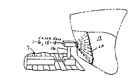
Fig. 6 is a schematic illustration of a portion of
substrate, which may be a ship's hull, that is being subjected
to this method of protection by the application of an
exceedingly smooth, pin-hole free, non-corrosive, coating of
fluorocarbon material, by the use of a laser fusion technique.
The controls of the previously described laser will cause the
laser beam to traverse many desired patterns while fusing the
fluorocarbon coating to the substrate. One such pattern
employed with excellent results is known as the "Lissajous"
pattern, identified at "LP" in the drawing Figs. 6 & 8.
Fig. 7 is a schematic illustration of cross-section taken,
through the substrate and coating at the target area during
laser fusion, for the purpose of approximating the power
distribution between the coating layer and the substrate and
interface regions. In this figure, the following definitions
need to be observed:
R1 - Refle~~ted IR laser beam radiation back from the
coating surface, measured in percent.
R2 - Refle~~ted IR laser beam radiation back from the
substrate and into the coating, in percent.
A1 - The level of absorption by the film, measured as a
percent per centimeter of thickness of the coating (or film).
CA 02070776 2000-04-11
-14-
A2 = the level of absorption of the substrate to the laser
beam, measured as a percent with respect to reflectivity and
transmissivity. The formula for this relation is: A2 - L1 -
R1 - A1 - R2.
D1 = The thickness of the coating measured in mm.
D2 - The depth of heat penetration into the substrate.
Using the above factors, the approximate total power
delivered by the laser beam L1 should be sufficient to
accommodate the energy utilized in generating the following
conditions: Total Power = R1 + A1 + R2 + A2.
Fig. 11 (i.e. Figs. 11A-11D) represents the internal
circuitry of the analog and digital conversion interface unit
9 of Figs. 1, 2, & 10 and discloses the circuit relationship
between each of the incoming, outgoing, and internal signals
of block 9. In Fig. 11A, it is seen that a "Smart" carrier
board 9.1 contains and supports memory module 9.2 for high
speed capture of incoming analog to digital conversion (ADC)
data by the analog input module 9.3 for the central processing
terminal 10. This nigh speed I/0 module 9.3 (Burr Brown Part
No. PCI-20023M-1) is used to receive incoming analog telemetry
sensing signals or levels from the high speed telemetry
measuring subsy:;tem sensor 4 of Figs. 1 & 2, and from the
thermal feedback sensor level, which comes from unit 5 of Figs.
1 & 2, and from the IR camera peak temperature analog signal
which comes from thermal image processor 12. These signals are
captured in real time by the central processing terminal 10 and
will be used by the supporting software for the correct
manipulation of t=he entire system by way of values obtained via
the Max laser power register unit 9.4C and the Max laser head
speed register 'unit 9.4F, as well as from the X & Y scan
pattern rates of unit 9.8A, and from the Galvo optical
corrector memory map stored in unit 9.8B of Fig. 11B.
Fig. 11A also contains PC Board 9.4 which can generate up
to 8 analog output channels with total throughput of 31, 200
outputs/sec. or up to 3900 outputs/sec. per channel. Output
values are supplied by central processing terminal 10 for Min.
T° register DAC 9.4A, for minimum temperature comparison for
CA 02070776 2000-04-11
-15-
thermal feedback of sensor 5, and for Max T° register DAC 9.4B
for maximum temperature comparison for thermal feedback sensor
5, and for Max power register DAC 9.4C, for the maximum laser
power allowed, temperature to power gain control signal DAC
9.4H, for controlling the gain of the delta between Max T°
register temperature value and actual temperature measured,
which in turn controls the laser power modulation output from
amplifier 9.10 to laser power supply unit 8, when the
temperature falls between minimum and maximum set values for
this system.
Also from unit 9.4, signals for monitoring and
manipulating the laser head speed will be done, by supplying
DAC analog levels for IR Min register DAC of unit 9.4D which
is for referencing the minimum peak temperature value; IR Max
register DAC unit 9.4E, which is for referencing the maximum
peak temperature value; Max laser head speed register DAC 9.4F,
which is for referencing the current maximum speed for the
laser head movement, and IR camera peak temperature to laser
head speed control gain register DAC 9.4C, which is for
controlling the gain of the temperature delta between the
maximum peak temperature reference and the measured peak
temperature thru the circuit of unit 9.15.
There are additional circuits that are added outside of
the PCI boards that further control the supplied signal levels.
There are two cornparators 9.9 that compare minimum and maximum
temperature values with incoming high speed temperature
measurements made by sensor 5 and the result of these two
comparators are used to properly address an analog multiplexes
unit 9.11 which i.n turn selects which correct analog level will
be supplied to the laser power modulation input of unit 8, from
amplifier 9.10; for example:
INPUT A1 AO Description of selection result:
INO 0 0 Output = Max Laser Power Reg. DAC 9.4C
IN1 0 1 Output - Temp. to Laser power conversion
output 9.16
IN2 1 0 Output = Ov
CA 02070776 2000-04-11
-15a-
IN3 1 1 Output = Ov
In Fig. 11F3, the General Scanning System shows that it
supports RAM driven DACs that drive limited turn servo motors
2 & 3 for X & Y galvo mirror drivers from electronic unit 9.8A,
along with RAM driven DACs that drive galvo-optical corrector
positioners from electronic unit 9.8B. This system is also
controlled by central processing terminal 10.
In Fig. 11C the temperature to laser head power conversion
is done by taking the difference between real time analog level
or signal TFS, from the thermal feedback sensor 5 complemented
through Z7 who'~~ gain is equal to -(R19/R18) and subtracting
this level or signal MXTR from Max T° register DAC of 9.4B
(MXTR) through operational amplifier Z1 which results in an
output equal to (R2/R1)*(MXTR-Z7 output) while assuming R1=R3
and R2=R4. The resultant level is then passed on to op amp Z2
for positive amplificaiton where the output gain is equal to
(1+(R6/R5)), but. modified by Q3's parallel resistance. This
resultant output. is then amplified again by op amp Z3 which
results in a gain of -(R8/R7). The resultant of this output is
then added to analog level (MPR) through op amp Z4 which
results in a gain of - ( (R12/R10) * (23output) + (R12/R11) * (MPR) ) .
The resultant of: this output is then passed on to op amp Z5
where the analog level is turned back to being positive again
with the resulting gain of -(R15/R14). The meaning of this
circuit can be summerized with the expression: ((MXTR-
TFS*Z7)*Z1*Z2*Z3+MPR)*Z4*Z5) where the "*" is the
multiplication factor of the amt~lifiers.
35
V1'O 91 /05885 PCT/US90/0309?
~'~~D'~'~ 6
In Fig. 11D, an analog level is supplied by IR Thermal image
processor 12 of Fig. l b ?; this analog level of IRI'T', represents the peak
temperature over the treated surface and is compared to IRMIi~ and IRMAh
analog reference levels from units 9.4D and 9.4E using comparators Z8 6 Z9
of unit 9.9, which in turn addresses the correct input for analog multiplexes
which supplies the current laser head speed level LHSL to amplifier Z10, and
unit 9.17 via unit 9.15.
In the event that the peak temperature signal IRPT is below IRMIA
and IRMAX then the output analog multiplexes level LHSL from unit 9.17 uill
equal Ov.
In the event that the peak temperature signal IRPT is greater than
IR'~IIN, but less than IRMA.X, then the difference of IRMAX and I1;PT is taken
and amplified by op ar~p Z1 who's output will equal (R2/R1)*(IkMAX-1RPT),
whic~~
in turn will be positively amplified by Z3 who's gain will equal (1+(R6,~R5))
1~ but modified by the parallel resistance of Q3. This result will in turn b=-
amplified again by Z3 with a gain of -(R8/R7). That result in turn will be
added to the Max Laser Head Speed register DAC 9.4F output signal MNSR, usinE
summing amplifier Z4 who's output will equal -((R12/R10)*(Z3output)+(R12/R11)
*tiHSR). The result of this level will be returned back to its positive ie~:el
z~~ value with op amp Z5 who's gain will equal -(k15/R14). This value will be
brought to IP;1 of analog multiplexes 9.11 that supplies si~;ual LHSI. to
ampllfir:
Z10 and to laser head speed level ~~it 9.15, and laser head speed control unit
9.17. Therefore, the meaning of this circuit can be summerized by the
expressi:>r;v
((IRMAX-IKPT)*Z1*Z2*Z3+riHSR)*Z4*Z5 where tl~e "*" is the multiplication
factor
~~ of the amplifiers.
In the event that IR peak temperature exceeds both IRMIN and IRMAX
then the output signal of Max laser head speed register DP.C unit 9.4F, whi::h
is the MHSR value, will be applied thru block 9.15 and to laser shutter
control
functional unit 9.18, located in unit 8, and its signal LSC will send a logic
30 "0" to subsystem 8 for causing shutters 7.11 to be closed.
Digital I/0 shutter control signals DIOSC and DIOSE frcu~ unit 9.8
can override the peak temperature to laser head speed level conversion :nutter
control signals from units 9.13 and 9.74, to temporarily shut down the systeTo
via output signal LSC when the peak temperature is too excessive too
frequently.
3~ In summary, one example of the steps forming tl~e final protection
coating C2, include:
t r T l _...W__ .__ .
1'VO 91 /0588
PCT/L S90/0309 i
2Q'~0'~'~6
1. Prepare target surface 13 by sandblasting the surface with san~!'
particles that are the approximate size or multiple size of tt;c IF:
wavelength
to be used.
2. Focus the radiometer of camera 11, onto the target surface to be
treated.
3. Determine the proper emissivity of the surface to be treated b
referring to the radiometer manufacturer's reference manual on known
emissivity
values for known surface materials. However if the surface material is
unknown;
then with all lights out and the surface kept from any type of wind or breeze,
place a precision thermal measurement probe on the unknown surface and view
this
same surface area with the radiometer cameras. Then adjust the emissivity
value
up and/or down until the radiometer measures the same temperature as the
ther~~r'
probe. When the two temperatures match, this represents the correct
emissivir~r
value of the unknown material at roo~a temperature. Some materials exhibit
different emissivity values at different temperatures, therefore, it is
advisable
to confirm the emissivity value again at normal process temperature and use
this latter value, if different.
4. Adjust the thermal feedback sensor's emissivity value up and!or
down while measuring the target's surface temperature with the radiometer and
comparing the two values. hhen these two values match, the correct emissivit:
value has been found for the thermal feedback sensor.
5. Apply the initial powder coating, which is PFA, in this example,
to target surface 13 which is 2mm thick mild steel, by setting the
electrostatic
sprayer charge to 80kv and then spraying the target surface until a fixed even
thickness layer builds up.
6. Set the laser head itself to a distance of 1 meter from target.
7. Set the maximum output power of laser 7 to 150 watts.
8. Set the Max power register 9. to 140 watts.
9. Set the Max T° register limit to 360°C.
10. Set the Min 1'° register limit to 330°C.
11. Set the IR Max register 9. limit to 360°C.
12. Set the IR Min. register 9. limit to 342°C.
13. Set the Max head speed register 9. to lcm/sec.
14. Select program software for a scan width of 5cm sawtooth.
15. Select program software ofr a.scan height of 5cm sawtooth.
16. Select program software to maintain a beam diameter of ? mm at
current target surface distance.
._ ~ 2070776
-18-
17. Select program software for a "X" axis scan rate of
66.67Hz.
18. Select program software for a "Y" axis scan rate of
50.OOHz.
19. Activate laser shutters 7.11 through software control
via terminal 10.
20. When target temperature reaches 342°C then apply
second coat.
21. When the current coating melts, set the electrostatic
spray gun to 100Kv and apply another spray burst.
22. Each successive coat adds O.lmm of thickness.
23. Continue until desired thickness is achieved. (i.e.
2mm in one example ) .
24. When the last coat melts, select program software to
reduce heat and close shutters, thus shutting off laser 7.
25. The finished surface will shortly acquire a glossy
finish that is pinhole free and possesses increased aqualous
slip, and increased resistance to corrosion and other
environmental or man-made hazards.
An itemized list of the principal operating components of
the system of this invention is shown in Exhibit A, attached
hereto.
From the foregoing description and examples it will be
seen that there has been produced a process and an apparatus
that substantially fulfills the objects of this invention as
set forth herein. These inventions are not limited to examples
shown herein, but may be made and performed in many ways within
the scope of the appended claims.
35
C
___ 207077fi
-18a-
Reference Part name or Designation/Manufacturer's Part
Number No./Mfg. or Supplier
1 Galvo Optical Corrector/EVK500 & EZ450/Laser
Lines, Ltd.
2 "X" Axis Scanning System/EXY3037 & EWK300/Laser
Lines, Ltd.
3 "Y" Axis Scanning System/EXY3037 & EWK300/Laser
Lines, Ltd.
4 Telemetry Measuring Sub-system:
Laser Light Source/lOR-TX/Metax
Telemetry Sensor/2L10/SiTek
Thermal Feedback Sensor/J15D5-M204-SO1M/EG & G
Judsons
6 Laser Power Sensor/J15D12-M204-250U/EG & G
Judsons
7 Laser/PRC1500/PRC Corporation
8 Laser Power Supply & Signal Input/(Included
with Laser, Ref. #7)
9 Analog & Digital Conversion Interface (Decimal
#'s represent functional and/or physical units
as appropriate):
9.1 Smart Carrier Board/PCI-20202C/Burr Brown
9.2 Memory Module/PCI-20201M/Burr Brown
9.3 Analog Input Module (ADC)/PCI-20023M-
1/Burr Brown
9.4 Analog Output Module (DAC)/PCI-20093W-
207077fi
-18b-
1/Burr Brown
9.5 PC Buss Expansion Box/PCI-20055H-4/Burr
Brown
9.6 PC Buss Interface/PCI 20063A/Burr Brown
9.7 Digital I/O Shutter Control/PCI-20087W-
1/Burr Brown
9.8 Dual Axis Scanning Sub-System/(Included in
Ref. Nos. 2 & 3)
9.8A X & Y Scanner Electronics (Included in
Ref. Nos. 2 & 3)
9.8B Galvo Optical Corrector Electronics
(Included in Ref. No. 1)
9.9 Comparator including TTL
Output/LM311/Texas Instruments
9.10 Operational Amplifier (Op Amp)/LM318/Texas
Instruments
9.11 Analog Multiplexer {MUX) 1 TMS 6005 & SN
7442/TI
9.12 NAND Gates/SN74LS00/Texas Instruments (TI)
9.13 AND Gates/SN74LS08/TI
9.14 Four Input NAND Gate/SN7420/TI
9.15 Printed Circuit Board (PCB)
Assembly/(Laser Head Speed function)
9.16 PCB/(Temperature to laser Power Conversion
function)
9.17 PCB/(Laser Head Speed Control Function)
9.18 PCB/(Laser Shutter Control Output
function)
Central Processing Terminal/Industrial
80286/Zenith & Heath
11 IR Camera/Probeye 7000/Hughes
12 Thermal Image Processor/Probeye 7000/Hughes
C
._ ~ X070776'
-18c-
13 Surface Application (Target)/PTFE, PFA, FEP,
TFE, ETFE, PVF, CTFE/DuPont, et al
14 Telemetry Reflection (Beam Spot)/Not Applicable
15 AU or CU Plated Mirror (for IR Optics)/12 MFC
007/Melles Griot
16 Beam Delivery & Formating System:
16.1 Beam Delivery IR Wave Guide/Per Customer
Specifications of distance from Laser to
Laser Head/Johnson & Johnson
16.2 Beam formating optics/Per Customer
Specifications of power density at distant
target and beam footprint shape/Melles
Griot or Laser Power Optics Co.
17 Beam-IR View Spot Combiner Optics/Per Customer
Specifications of lens with maximum
transparency for IR wavelengths of 8.5-12.0 um
and maximum reflectance for IR wavelengths of
2.0-8.5 um./STC Components, Ltd.
18 Beam-Telemetry Combiner Optics/Per Customer
Specifications of lens with maximum
transparency for IR wavelengths of 2.0-14.0 um
and maximum reflectance for IR wavelengths or
0. 4-2 . 0 um. /STC Componants, Ltd:------------------ ,
C