Note: Descriptions are shown in the official language in which they were submitted.
~~ ~~>ossn9 1 ~ ~ ~ ~ ~~i ~. ~ca~ius~oios~~~
WAVESHAPING TRANSVERSAL FILTER AND METf-IOD UTILIZING THE SAME
FOR DATA TRANSMISSION OVER COAXIAL CABLE
BACKGROUND
This invention relates generally to a pulse shaping
transversal filter which can be used in lieu of an equalizer
in equipment coupled to a coaxial cable. The invention more
particularly relates to a transversal filter for creating a
raised cosine wave which is transmittable over a coaxial cable
to a network interface without requiring line build-.out. The
invention has particular application to transmittal of data in
the DS3 format, although it is not intended to be so limited.
According to present standards, a data communications
pulse being received at a network interface over a coaxial
cable of up to four hundred fifty feet long must eomply with a
certain shape and amplitude as set forth in TlE1/88-00681
dated July 1988. Traditionally, the transmitted pulse shape
is in the form of a square wave, and massaging of the pulse is
r~quixed to,assure compliance with standards. The standard
mans for performing the massaging is '"line build.out" as is
v~ell knhwn ~in the art.
SUMMARY OF THE INVENTION
ii'~D ~i/08f~~19 ~ 2 P(.°flvS90/06~~2
network interface regardless of cable length (up to 450 feet).
The proper pulse shape which obviates line build out is a
raised cosine, or a pulse in substantially a raised cosine
format. Thus, the broad method of data transmission over a
coaxial cable is to obtain an input wave, to filter the input
wave according to a preset filter so as to produce a
substantially raised cosine waveform, and ~to transmit the
substantially raised cosine waveform over any coaxial cable of
up to four hundred fifty feet to the network interface.
The substantially raised cosine waveform is obtained from
the transversal filter. The transversal filter has a standard
pulse shape input. The standard pulse is then shifted a given
increment in tame, weighted, and added to itself. This,
procedure is repeated a number of times to arrive at the
desired output waveshape suitable for transmission over the
coaxial cable.
It is therefore an object of the invention to provide a
method and apparatus for transmitting data over a coaxial
cable without provision for line build-out.
It is another object of the invention to provide a method
and apparatus for generating a substantially raised cosine
pulse shape suitable for transmission over coaxial cable of
lengths up to four hundred fifty feet without equalization.
It is a further object to provide a transversal filter
capable of generating substantially raised cosine pulses
suitable for bipolar data transmission of a coaxial cable,
. WO 91/QS549 3 ~ 2 ~~~ ~~~ ~ ~ P("T/US90/06~92
The transversal filter in accord with the objects of the
invention broadly comprises a plurality of variable delay
lines each having multiple stages in series, with one of the
variable delay lines having a clock input, and at least one of
the variable delay lines having data signal inputs, a phase
comparator coupled to an output of the variable delay lines
with the clock input, a feedback circuit coupled to the
comparator and to each of the variable delay lines, and a
plurality of weighting circuits coupled via switches to each
of the variable delay lines having data signal inputs. Each
stage of the variable delay line has at least one transmission
gate and at least one inverter in series, and preferably two
of each. The phase comparator compares the phase of the
signal exiting the variable delay line with the phase of the
signal entering the variable delay line arid provides a signal
indicative thereof. The phase comparator signal is averaged
and averaged/inverted by the feedback circuit, and the average
and inverted average are fed back to respective gates of each
transmission gate of the multiple stages of each variable
delay line to control the speed at which data passes though
the stages. As a result, data (or clock) signals passing
through eaci~ stage of the variable delay line are an equal
fraction of a cycle delayed at each stage such that the phases
compared at the phase comparator are equal. Taps from each
stage of the variable delay lines with data signal inputs are
routed through the weighting circuits which weight the signal
according predetermined weights so as to provide a
substantially raised cosine waveform.
Where the signal is a nS3 signal at a frequency of
approximately 44.736 MHz, and coded according to the B3ZS
code, data must be sent as positive data, negative data, ar
zero data. As a result, four variable delay lines having
multiple stages in series are preferably provided; one each
for the positive (i.e. 5V), negative (i.e. ~V), and zero data
(i-.e. 2.SV), and one for the clock. Only the variable delay
line for the clock has a phase comparator and feedback
CA 02070811 2000-O1-17
72235-21
4
circuit. The feedback voltages generated from the feedback
circuit of the clock circuit are fed to the transmission gates
of all of the variable delay lines to guarantee equal delay
through each stage of the variable delay lines. Taps off each
stage of each variable delay line are then fed through switches
. to the weighting circuits which are basically voltage dividers.
Taps off the stages of the variable delay line for the clock
circuit are also subject to switches for purposes of providing
equalizing capacitance, although those switches are not
connected to the weighting circuit.
In accordance with the present invention, there is
provided a transversal filter for taking a square wave clock
signal and at least two different data value signals indicative
of a desired signal, and creating a substantially different
waveform representing said desired signal therefrom, said
transversal filter comprising: a) at least three delay lines
each comprised of at least three substantially identical stages
in series, each stage having a voltage controlled delay means,
a first of said delay lines coupled at its input to said clock
signal, and second and third of said delay lines to respective
of said two different data voltage value signals; b) phase
comparator means coupled to the clock signal delay line at the
outputs of two different non-adjacent stages of the clock
signal delay line, for comparing the phases of signals at said
outputs and providing at least one feedback signal indicative
thereof; c) feedback circuit means coupled to said phase
comparator and to said voltage controlled delay means, for
applying said at least one feedback signal as at least one
voltage control signal to each voltage controlled delay means
of each stage of each delay line, whereby said at least three
delay lines are thereby calibrated such that each corresponding
stage of each delay line is an equal fraction of
CA 02070811 2000-O1-17
72235-21
4a
a clock cycle delayed in time relative to a preceding adjacent
stage.
In accordance with the present invention, there is
further provided a method for transmitting encoded digital data
over a coaxial cable of desired length without providing for
line build-out, comprising: a) obtaining a digital data signal
with an associated clock signal; b) encoding said digital data
and providing as a result thereof at least three outputs
indicative of when a positive pulse is desired, when a negative
pulse is desired, and when a zero pulse is desired; c)
filtering said positive, negative, and zero pulses, with a
waveshaping transversal filter having said clock signal as
another input thereto, so as to produce a substantially raised
cosine waveform; and d) transmitting said substantially raised
cosine waveform over said coaxial cable without providing for
line build-out.
Additional details and advantages of the invention
will become apparent to those skilled in the art upon reference
to the detailed description taken in conjunction with the
provided Figures.
BRIEF DESCRIPTION OF THE DRAWINGS
Fig. 1 is a block diagram of an apparatus for taking
a square wave and producing B3ZS substantially raised cosine
waves therefrom;
Fig. 2 is a detailed block diagram of a portion of
the transversal filter of Fig. 1;
Fig. 3a is a detailed block diagram of the multiple
stage variable delay line and associated switches which are
part of each block of Fig. 2;
i~0 91f085~89 5 ,. , . - .. p~/US~O/06~92
Fig. 3b is a schematic diagram of the a single stage of a
variable delay line;
Fig. 4a is a wave shape diagram showing the permissible
pulse shapes at a network interface as defined by
T1E1/88-09681; and
Figs, 4b - 4d are respectively a wave shape generated by
the apparatus of Figs. 1-3, and resulting waveforms received
at a transmission network interface (9 feet), and after
transmission through a 129 foot and a 450 foot coaxial cable.
DETAILED DESCRIPTION OF TEIE PREFERRED EMBODIMENTS
The preferred apparatus as seen in Figures 1-3 relates to
a device which receives a DS3 signal which includes data and
clock, and which generates a substantially raised cosine
waveform in B3ZS format for transmission over a coaxial cable
to a network interface. For purposes herein the term
°'substantially raised cosine°° means any waveform which
is
intended to approximate a raised eosins or a similar wave in
shape, or any waveform which ma y be transmitted over coaxial
cables of lengths up to four hundred fifty feet and still meet
the T1E1J88=09681 standards for a network interface pulse w
shape without additional shaping, It will be appreciated by
those skilled in the arts, that the apparatus and methods
disclosed herein may be useful for other waveforms required by
other standards, and there is no intent that the invention be
limited to only DS3 signals, or to the B3ZS convention.
W~ 91 /88549 ~ ~ ~~ ~ ~ ~ 6 '~CT/US9~106892
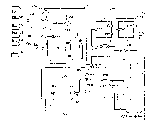
As seen in Fig. l, the apparatus lg of the invention is
comprised of the transversal filter 20, and associated
feedback circuitry 25, with additional prefiltering and post-
filtering circuitry provided, including a prefiltering
multiplexes 32, B3zS format block 34, and logic block 36, and
a post-filtering voltage regulating circuit 40. The
prefiltering circuitry basically instructs the transversal
filter as to whether it should output a positive or negative
substantially raised cosine pulse, or a zero pulse. As will
be described hereinafter, for a B3ZS raised cosine signal,
four variable delay lines are desired in the transversal
filter 2~, with each delay line comprised of four or more
stages. All of the delay lines should be located on the same
integrated circuit chip to help guarantee identical parameters
and delay.
In the preferred embodiment, the multi,plexer 32 is
provided as the interface into the circuit. Multiplexes 32 is
standard in format. It receives data and clock inputs 42c,
424, and 43c, 434 in DS3 square wave format from two sources,
and uses a control input 45 to determine which of the data and
clock input pairs is to be passed alone, The outputs of
multiplexes 32 include the square wave data signal 48, and two
clock signals 52 and 54 (csn and cmn) of alternate polarity,
but of the same frequency as the chosen clock input.
The data and clock signals output from the multiplexes 32
are fed to an 83ZS encoder 34 of standard format. The B3ZS
encoder takes the incoming signal and generates a data output
56 and a sign.szgnal 58 which are based on the incoming data
and which comply with the B3ZS coded format. The B3ZS encoder
is clocked according to the two phase clock pair cmn.and csn.
W~ 9l/08s~99 7 ~. . ~ PC1'/AJS90/~6Fd92
The data and sign outputs of the B32S encoder (as well as
ClUCk cmn) are forwarded to the logic block 36 which outputs
one of three possible signals in response thereto. Tf the
data signal 56 is a '°1" and the sign signal 58 is a "1'°, the
logic block 36 produces a pulse indicative of a positive
signal (tplus) at 60. If the data signal 56 is a "1", and the
sign signal 58 is a °'0", the logic block 36 produces a pulse
indicative of a negative signal (tgnd) at 62. Finally, if the
data signal 56 is a "A", the logic block 36 produces a pulse
indicative of a zero signal (tref) at 64, regardless of the
value of the sign signal 56.
The pulses indicative of positive, negative, and zero
signals are all coupled to the transversal filter 20 of the
invention. Other inputs into the transversal filter 20
include a reference voltage vref (e.g. 2.5V) obtained from a
voltage source 65, an input clock 54 Belated (via clock cmn)
to the input clock into the multiplexes, and as will
hereinafter be described, feedback voltages 7A and 72,
Turning to Figure 2, additional detail of the transversal
filter is seen. Basically, the transversal filter 20 is
comprised of four internally identical blocks llAa, ll~b,
21~c, and 1104. Each block 110, however, has different signal
and voltage inputs, as well as different output line
connections. The signal input into block llAa is clock 54,
and the voltage input which controls the output voltage of the
output signals of block llAa is tied to a positive voltage ._
rail Vdd (not shown). The data input into block ll~b ~.s the
positive signal pulse 6A, and the voltage input is also tied
to the positive voltage rail. The input into block llfdc is
the zero or reference signal pulse 64, and the voltage input
is tied to the voltage source 65. The input into block 1104
is the negative or ground signal pulse 62, and the voltage
w~ ~nos;~9 ~ '~ ~ g~ ~. ~- 8 ~~ri~~~oio~s~z
input is tied to ground. The outputs of blocks 110 will be
described hereinafter.
The internals of each block 110 is seen with reference to
Figure 3a where a six stage delay line is seen. The first and
last stages 120a and 120f are preferably buffer stages, and
stages 120b - 120e act to provide delay outputs as will be
described hereinafter. Each stage 120 includes a delay
circuit 125 which is shown in Figure 3b, as well as a switch
128 which permits the voltage associated with the particular
delay line to be switched to the voltage divider circuit.
Referring to Figure 3b where the details of the preferred
delay circuit are seen, each delay circuit preferably
comprises a CMOS transmission gate 132 having an n-type and a
p-type CMOS transistor in parallel, followed by an inverter
134, followed by another CMOS transmission gate 136, followed
by another inverter 138. As indicated, the feedback voltages
70 and 72 are applied to the respective gates of the n-type
and p-type CMOS transistors. The application of a voltage
difference across the gate leads of the CMOS transmission
gates controls the delay through the transmission gates 132
and 130; as CMOS device are voltage sensitive. By providing a
plurality of the delay circuits of Fig. 3b in parallel as w,
shown in Fig. 3a, a single variable delay line is provided.
As shown in Figure 2, block 110a, which has the DS3 clock
as its data input, has two outputs 141 and 143 which are
related to the phase of the clock signal as tapped from
locations shown in Figure 3a. In particular, the DS3 clock
signal is loaded into buffer stage 120a which basically
experiences no delay as a 5V voltage difference is applied to
the gates of the n-type and p-type CMOS transistors which help
constitute the buffer stage. The buffer stage 120a (as well
.. d~'~ 91/ID~54~ c~ ' F'CT/U~9~/06~92
as output buffer stage 120f) is provided so that the other
stages 120b ~ 12~e will see equal input arid output impedances
(i.e. for balancing). Because buffer stage 120a provides no
delay, the output of stage 120a is considered to be at time
zero in the cycle of a single clock pulse (i.e. t0 = 0). The
clock signal from the data output of stage 120a provides a
first phase detection point and provides phase output 141. As
the clock signal is transferred down the array of stages, the
signal is delayed somewhat due to the voltage difference
across each transmission gate not being a full five volts.
The output from the fifth stage 120e, which provides four
delay times, is taken as the second phase output 143. The
phase outputs 141 and 143 are then compared by a phase
detector 150 (see Fig. 1) which is part of feedback circuitry
25.
Phase detector 150 compares the phases of the signals
from the output of stages 120a and 120e, the signal from one
of the stages being inverted prior to comparison, and provides
a signal in response thereto. The signal is provided to the
RC eircuit comprised of resistor 152 and capacitor 154 which
is coupled to ground. The RC circuit takes the pulse from the
phase detector 150 and provides an average direct current
signal. The dizect current-signal is then provided to an op
amp 156 of unity gain which serves to buffer the RC circuit
from block 110a. The output of op amp 156 is fed to an
inverting op amp 158 (having gain of minus one provided by
resistors 161 and 163) as well as to the gates of all n-type
transistors of transmission gates 132 anc~ 136, while the
output of op amp 158 is fed to the gates of all p-type
transistors of transmission gates 132 and 136. In other
words, the feedback circuit 25 coupled to block 110a, is used
to create feedback voltages which are applied to all
transmission gates of each stage of each block where delay
ti~rough the stage is desired.
i~'~ 9! JOf35d9 ~ ~ ~ .~ ~ 1 ~ PC:TlUS9iD/06892
As in most feedback type circuits, the goal of the
feedback circuit 25 is to stabilize the transversal filter.
Stabilization occurs by eliminating any phase difference
between the phases of the signals being received at the phase
detector 150. When the phase difference is eliminated such
that the phase at the output of stage 120a is the inverse of
the phase at the output of stage 120e, the feedback circuit is
in equilibrium. In equilibrium, the clock input into block
110a is delayed by equal fractions of a half a clock cycle by
each stage 120 provided each stage of the block is identical
and has identical output impedances. Fecause the transversal
filter circuit is an integrated circuit, the make-up of each
stage is guaranteed to b~ virtually identical. Also, by
providing identical switches 128 coupled to each stage 120,
the impedances on the outputs are guaranteed to be virtually
identical. Thus, where four stages are provided as part of
the delay line (after the initial buffer stage 110a and before
the terminating buffer stage 110f) as in the preferred
embodiment, the clock signal at the output of each stage 120
is one eighth (i.e. one quarter of one half) of a clock cycle
removed from the clock signal at the output of the preceding
stage. If five active stages were provided, the clock signal
at each stage would be orse terwth of a clock cycle remaved from
the clock signal at the preceding stage. Regardless, stages
of.equal fractions of a clock delay are generated and are used
as a calibration for the delay lines not. having the feedback
circuit.
Returning to Figure 3a, it is seen that switches 128 are
CMOS switches which are provided with three inputs and a
single output. A first input inta switches 128 is the supply
voltage as discussed with reference to Figure 2. The second
and third inputs are voltage inputs from corresponding stages
of the delay line which are sent to the n and p gates of the
CMOS switch. As the data pulse into the delay line propagates
through the delay line, on the leading edge of the pulse, the
associated switch 128 is turned on, while an the trailing edge
WO 9i/086~39 11 ... ~ P~/1J~90/06892
of the pulse, associated switch 128 is turned off. mhos, as a
data pulse propagates through a delay line, the supply voltage
provided to switches 128a - 128e is provided at the output of
the switches during the length of the data pulse. Because the
data pulse is delayed, the voltage at the outputs of each of
switches 128a - 128e are delayed one eighth of a clock cycle
with respect to the previous adjacent output.
Each of the switches 128 of delay lines 110b, 110c, and
110d are coupled to the post-filtering voltage regulating
circuit 4g which essentially comprises a voltage summing and
divider circuit, and acts in conjunction with the signals
output from the delay lines to shape an output wave. As seen
in Figure 2, each output from delay lines 110b, 110c, and 110d .
is sunuued with outputs from the other delay lines which
correspond in time delay; i.e. the t0 outputs are all
connected, the tl outputs are all connected... The summed
outputs are fed through parallel resistors 180-0, 180-1,
180-2, 180-3, and 180-4 which act as the first resistor~in a
voltage divider with resistor 19~ whidh .is coupled to the
reference voltage of 2.5V. By appropriately choosing values
for resistors 180 and resistor 190, a substantially raised
COSin° waveform can be generated. For sake of completeness,
it should also be notad that another resistor 193 is provided
in parallel with resistor 190 to cause the amplitude of the
output voltage txout to decrease for short lines. Thus, a
control signal txlev 199 (transmit level) is provided as an
input to switch l96 and inverter 197. When txlev 199 is Iow,
switch 196 turns on and effectively planesresistor 193 in
parallel with resistor 190. When txlev is high, switch 197
turns off and effectively provides an infinite resistance,
such that the resistance of resistors 190 and 193 in parallel
is equal to the resistance of resistor 190.
WO 91/03549 . : _ P~'f/U590/06892 r,~."
12
According to the preferred embodiment of the invention
resistors 180 and resistor 19g are chosen such that the
relative conductance values of resistors 180-0 through 180-4
are 0.7, 0.5, 1, and .7 respectively. These values are then
scaled to the conductance of resistor 190 to give an
appropriate output voltage. With these conductance values, it
has been found via numerical summations that a substantially
raised cosine waveform is generated with both polarities with
the provided delay lines having outputs of five volts (Vdd),
two arid one half volts (Vref) , arid zero volts (gnd) . In
particular, the output voltage txout front the voltage
regulating circuit 40 is determined according to the following
equation:
txout = _ tn/R(180-n) + Vref/R(19g)
~(1/R(190)] + ~l/R(180-n)~ [1/R(19~)] +~1/R(180-k)
k.o
where tnnis the voltage output from the n'th stage o.f the
active delay line switched via switch 128n, and R( )
symbolizes the resistance of the appropriate resistor 180-0
thraugh 180-4 or resistor 190. The sum in the denominator is
simply the sum of the conductances of resistors 180 plus the
conductance of resistor 190. By way of example only, if the
denominator has a value of ten mhos,' the numerator is the
voltage value of.a given output tn weighted with the
conductance of its connected resisto r. Txout is referenced to
a fraction of Vref since resistar 190 is connected to vref and
not to ground, Assuming a zero pulse signal as a starting
point, where block llfdc is providing Vref sequentially at its
autputs, the output voltage txout is. exactly 2.5 vols (Vref)
since there. is no current flow in any of the resistors 180.
Then, assuming a positive output voltage at time t~, the
voltage\at the t0 output of block 110b goes to five volts
(Vdd). The output is then defined according to the formula:
txout = (5x0.7/10) + (2.5x1/10) + (2.5x0.5/10) + (~.Sxl/10)
+ (2.Sxf.7/lfd), + (2.5x6.1/10)
or txout = 2.b75 volts.
y~~~fs~~
CVO 9 ~ /~85d9 13 P~ fliJS9~l~6f392
One eighth clock cycle later, the voltage at the tl
output of block 110b goes to 5V, follotF~ed by the t2 voltage
one eighth of a clock cycle after that, etc. By half a clock
cycle, when the positive pulse reaches a maximum, the voltage
at the tl - t4 outputs are all high, with the switch 128 at t0
stage of block 110b turning off as the switch at the t4 stage
110b and the switch at the t0 stage of block 110c (2.5V) turn
on. Thus, over half a clock cycle, the voltage at the output
of the voltage regulating circuit continues to climb from
2.675 to 2.925, 3.05, and 3.30 volts respectively for each
eighth clock cycle. Then, as the positive pulse propagates
through block 110b, in successive eighth cycles, the five volt
tl, t2, t3, and t4 outputs of block 110b are turned off, while
the two and one half volt outputs of tl, t2, t3, and t~ of the
block 110c are turned on causing the voltage to decrement
successively from 3.3 to 3.05, 2.925, and 2.675 volts until
the 2.5V "zero" pulse value is reached and the raised cosine
wave of a complete cycle is completed.
If the next pulse is another positive. pulse, the same
cycle is repeated. If the next pulse is a "zero pulse°', all
of the switches on the outputs of block 110c are sequentially
turned on again, and an even 2.5V signal is applied across all
of the resistors 180. If the next pulse is a negative pulse,
the outputs of block 110d are activated, with zero volts being
applied to resistors 180-0, 180-1... in succession, as the
2.5V values are successively switched off. As a result, as
the negative wave propagates through delay block 1104, the
voltage at the eircuit output decreases from 2.5 to 2.325,
2.075, 1.95 and 1.7 volts. Then, on the second half of the
negative square wave, where a °'zero" value is entered, the
2.5V outputs of block 110c are turned back on as associated
outputs of block 110d are turned off, and the voltage at the
circuit output increases from 1.7 to 1.95, 2.075, 2.325 and
2.5 volts. At the end of the negative pulse cycle, the
negative raised cosine wave of a complete cycle is completed.
bV0 9~/~S5d9 '~ PC~'/1JS9~/06592
Turning to Figures 4a - 4d, it is seen that the waveform
(Fig. 9b) generated by the circuit of Figures 1 - ~ and
transmitted through both a one hundred twenty foot coaxial
cable and a four hundred fifty foot coaxial cable, provides .
waveforms (Figures ~c and 4d) which fall within the pulse
shape guidelines seen in Figure 4a. Thus, a raised cosine
waveform, which was generated from three input voltages, and
from a transversal filter which generates four equal delays
per half cycle (effectively creating a sampling at eight times
the clock rate), can be sent over any coaxial cable meeting
published specifications such that the signal received at the
network interface meets published specifications.
There has been described and illustrated herein a
transversal filter for creating a raised cosine wave which is
transmittable over a coaxial cable to a network interface
without requiring line build-out. The method invention is
closely related thereto. While particular embodiments o.f the
invention have been described, it is not intended that the
invention be limited thereby, as it is intended that the
invention be broad in scope and that the specifications be
read likewise. For example, while the invention was described
with relation to a B32S encoded DS3 signal, it will be
appreciated the invention applies to other square wave input .
signals> Also, while three input voltages were utilized,
desired output signals can be created from two or more input
voltages. Similarly, while delay lines generating signals
one-eighth cycle apart were described, delay lines having
three or more stages for generating signals one-third or more
cycles apart may have useful application. Indeed, other types
of output signals can be generated. Further, while CMOS
switches and delay elements formed as transmission gates were
described and illustrated, those skilled in the art will
appreciate that different arrangements for delay e7.ements and
switches can be provided with CMOS technology, and other
transistor technology such as bipolar or F3iCMOS could be
utilized. Likewise, while particular relative values for
~'l'~ 9i10~549 1~ PC'f/iJ~90/06~9~
resistors were provided according to the preferred embodiment,
it will be appreciated that other relative values could be
utilized to provide a substantially raised cosine waveform.
Therefore, it will be apparent to those skilled in the art
that other changes and modifications may be made to the
invention as described in the specification without departing
from the spirit and scope of the invention as so claimed.