Note: Descriptions are shown in the official language in which they were submitted.
~`
-
2071170
BP.C~GROUND OF INVENTION~
The present invention relates to a printed
circuit board support frame for protecting and trans-
porting a printed circuit board in a shipping container
or for protecting the circuit board when handled ky
persons in the trade.
It is known to ship printed circuit boards in
corrugated cartons with form cushioning material and
sometimes also in plastic containers which are comprised
of a base shell which supports a circuit board in an
elevated fashion, usually by a contour ridge, and wherein
a cover or ~ top shell is positioned over the bottom
shell and abuts the rear sLde of the printed circuit
board to clamp it in the support frame. The component
side of the board is usually facing downwardly and spaced
from the bottom wall of the bottom shell. One or a
plurality of these support frames can be retained in a
shipping container in a stacked f~shion with the circuit
boards immovable therein due to the close spacing between
the side walls and top wall of the container(s).
S11MMARY OF INV13WTION:
As far as the clamp shell type of plastic
container is concerned the present invention relates to
an improved support frame of the above-mentioned type and
which is formed rom moldable material, such as plastics,
and wherein the need to provide a cover for the support
frame i5 eliminated thereby making the container less
expensive to produce while offering excellent shock
absorbing properties to the printed circuit board when
transported in a shipping container.
*
-- 1 --
-2- 207l l70
Another feature of the present invention is to
provide a printed circuit board support frame for protecting
and transporting a printed circuit board and wherein the
frame is molded out of a single plastic sheet and therefore
has no 1008e parts coacting therewith to retain the board and
thereby eliminating the risk of losing a part and rendering
the ~rame unusable.
Another feature of the present invention is to
provide a printed circuit board support frame for protecting
and transporting a printed circuit board and wherein the
printed circuit board is ouickly positioned and engaged and
disengaged from within the support frame.
Another feature of the present invention is to
provide a printed circuit board support fr~me for protecting
and transporting a printed circuit board and wherein the
frame can be used to protect the board whether positioned
within or out of a shipping container with the electronics
components of printed circuit boards facing upwardly within
the support frame making them visible to the user znd wherein
the support frame is ~tackable one on top of another.
According to the above features, from a broad
aspect, the present invention provides a printed circuit
board support frame in combination with a shipping container
for protecting and transporting a printed circuit board. The
support ~rame is molded from suitable plastics material and
comprises a base wall section having elevated ~upport means
projecting rom a top face thereof for supporting the printed
circuit board elevated from the base wall section. The base
wall section has a hinged retention side wall member ~ormed
~long a pair of opposed parallel edges thereof. The
-2 -
-~ 207 1 1 70
retention side wall members, when hinged outwardly of the
base wall, permit the circuit board to be positioned on the
support means elevated from the base wall section. The
retention side wall members have one or more clamping means
to overlie opposed top side edge portions of the circuit
board when the side wall members are maintained in ~ vertical
positlon to clamp the circuit board over the support means.
The side wall members ~re maintained in the vertical position
by opposed vertical side walls of the shipping container.
Arresting means is provided to prevent the circuit board from
displacement .
BRIEF DESCRIPTION OF DRAWINGS:
A preferred embodiment of the present invention
will now be described with reference to the accomp~nying
drawings in which:
FIGURE 1 is n perspective view illustrating a
printed circuit board positioned in the support frame of the
present inventioni
FIGURE ~ is a top view of the printed circuit
support frame shown with the hinged retention side wall
members in ~ position of use to clamp a printed circuit board
therebetween;
FIGURE 3 is an end view of the printed circuit
~upport frame and which also illustrates the stdcl~ing
f eature;
FIGURE 4 is a section view across the printed
circuit support frame showing the configuration of the frame
and the positioning of a printe~ circuit over .I base wall
-3-
3~ 207 1 1 70
section of the ir~me;
FIGU~3 5 i9 a view similar to Figure 4 but showing
the hinged retention side wall members in a position of use
to clamp the circuit board;
, ~ f '~ ' '
-
." -3a-
' A
..~
. ".',~,
..... _~
2~7117~
FIGURE 6 is a section view through a shipping
container in which the support frame with the circuit
board clamped therein, is positioned; and
FIG[JRE 7 is a section view across the support
ribs formed in 'che base wall section.
DESCRIPTION OF PREFEF~RED EMBODIMENTS:
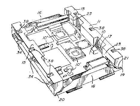
Referring to the drawings and more particularly
to Figure 1, there is shown generally at 10, a printed
circuit bodrd clampingly retained in a support frame 11
whereby to protect the circuit board while it is shipped
or handled by a person. The support frame 11 also
protects and offers shock absorbing properties, particu-
larly when positioned within a shipping container, as
shown in Figure 6. The printed circuit board support
frame as herein shown is molded from a single thin
plastic sheet by a thermoforming process, as is well
known in the art. The thin sheet provides flexible
properties to absorb shocks. The frame may also be
molded of other suitable material, such as pulp material.
Referring now additionally to Figures 2 to 7,
the printed circuit board support frame 11 has a base
wall section 12 which is a flat rectangular section
provided with elevated support ribs 13 formed in a top
face 14 thereof. The printed circuit board 10 is
disposed on these top ribs 13 and clamped thereon by
hinged retention side wall members 15 which are formed
integrally with the base wall section 12 along a pair of
opposed parallel edges thereof. P.t the opposed end edges
of the base wall section 12, there is provided stationary
abutment end walls 16 which are also formed with the base
wall section and extend transversely between the
-- 4 --
.. _ .
2071170
retention side wall members 15, as is better shown in
Figure 4~ The support frame 11 is custom-designed for a
specific circuit board to be shipped. It is pointed out
that the dimensions and configuration of the support
frame 11, the wall section 12, the support rib 13, and
top face 14, as well as wall member 15 may vary from time
to time in order to ~r- -,A ~te various printed circuit
boards . .
Elevated, spaced-apart abutment shoulders 17
are also disposed adjacent the elongated support ribs 13
and are elevated above the top face 18 of the suJ?port
ribs 13, as shown in Figure 4, whereby to retain the
circuit board 10 in close fit therebetween, as illus-
trated in Figures 1 and 5. The abutment end wall 16
constitutes arresting means to prevent the circuit board
from displacement in the transverse direction and
provides ease of positioning the printed circuit board
while packing. The board 10 is in close iit at its side
and end edges between the abutment shoulders 17 and the
abutment end walls 16.
Referring more specific~lly to Figures 4 and 5,
lt c an be seen that the retention side wall members LS
are formed integrally with the base wall section 12 but
spaced a predetermined distance along opposed side edges
thereoi. A straight creased hinge line 19 separates the
side wal~ members from the base wall and permits the side
wall members to be hinged towards the top face of the
base wa;Ll as shown in Figure 5. The base wall section 12
protrudes beyond the abutment shoulders 17 and have a
sloped edge wall 20 leaaing to the hinge line 19. The
side wall member 15 has an ad~acent sloped edge wall 21
. .
_ 5 _
_ _ _ _ _ _ , . .... . . _ . .
207117~
sloping upwardly from the hinge line 19 whereby these
sloped edge walls 20 and 21 are positioned in facial
arresting contact and form a strong ridge edge support,
as shown in Figure 7, when the retention side wall
members lS are maintained substantially upright, as shown
in Figures 5 and 7, in their position of use.
F~eferring again to Figures 4 and 5, it can be
seen that when the hinge retention side wall memhers 15
are hinged outwardly, the printed circuit board 10 can be
introduced to fit snugly over the elevated support ribs
13 between the abutment shoulders 17 and the abutment end
walls 16. When the circuit bo~rd i9 in this po6ition,
the opposed abutment shoulders 17 are hinged upwardly in
the direction of ~rrows 22 to clamp the circuit board.
As shown, the support ribs 13 are elongated ribs formed
along opposed parallel edge~ of the base wall section.
Each of the abutment wall members 15 are formed as a
casement and provided with clamping shoulders 23 which
proiect forwardly over respective one of the two
elongated ribs 13 when the side w~l 1 members 15 are in
their upright position of use. These clamping shoulders
23 each have a clamping notch 24 (see Fig. 4) in a lower
edge thereof to receive ~m edge portion of the circuit
board 10 to clamp the circuit board between the notch and
the elongated ribs 13.
The side wall members 15 are maintained in a
vertical positioll by an arresting me~ns which m~y be
constituted by the opposed side walls 29 of the
rectangular shipping container 30, as shown in Figure 6,
or by connecting tabs 34 described later. This container
also has a bottom wall 31 and a lockable hinged top wall
6 _ _ _ _
.~
2071170
or lid 32 with the hinge retention side wall members 15
of the support ~Erame 11 having a flat upper wall 15',
when in a vertical position. The side waIl members 15
are dimensioned for close fit between the top wall 32 and
the bottom wall 31. Accordingly, when the top wall is
closed, the support frame 11 is immovable in the
container and acts as a shock absorbing frame and spaces
the printed circuit board 10 intermediate the side walls
29, the end walls 33 and the bottom and top walls 31 and
32 of the shipping container 10.
As shown in Figures 4 to 6, the bottom wall
section 12 is also provided with two or more transverse
shock absorbing bumpers 28 formed integral therewith and
in a sp~ced-apart fashion, as better seen in Figure 2.
These bumpers provide shock absorbency and also
strengthen the bottom wall section 12 to give it
rigidity .
As illustrated in Figures 3, 4 and 5, the side
wall members 15 may be provided with two or more spaced
apart t~bs 34 for friction fit retention in aligned
c~vities 35 provided in the abutment wall 36 between the
hinge 19 and the shoulders 17. When the wall members 15
are r~ised to their vertic~l position, the tabs 34 are
press-fitted in their respective cavities 35 to retain
the wall member 15 upright with the circuit board in
position. This permits the boArd to be manipulated while
protected by the support frame.
-- 7 --
2Q71170
The cavities 35 also serve as a dual purpose in
that their outer surface 37 also constitutes legs which
are positionable ir, locating cavities 38 provided in the
top walL 15 ' of the side wall ~Lember 15 . ~his permits
for the stacking of two or more support frames 11 for
shipping, storage or other purpose.
Another advantage of the support frame 11 is
that the components 10 ' on the circuit board are facing
upwardly and are visible to the user, making the boards
readily identifiable without the need of having to flip
the support frame upside down, risking the danger of the
printed circuit board falling out of the frame.
It is within the 2mbit of the present invention
to cover any obvious modifications of the preferred
embodiment described herein, provided such modifications
fall within the scope of the appended claims.