Note: Descriptions are shown in the official language in which they were submitted.
2071~
G-7700 C-4340
FAULT DETECTION APPARATUS FOR A TR~NSFORNER ISOI~TED
TRANSISTOR DRIVE CIRCUIT FOR A POWER DEVICE
Thi~ invention relates to a power transisto.r
drive circuit in which the low level control logic
ci.rcuitry i~ transformer isolated from the power
transistor, and more particularly to circuitry
responsive to the occurrence of overvoltage and
overcurrent conditions.
Bac]cground of the Invention
Isolation transformers are used in
applications where low level logic components activate
high power switching devices. While the power required
to drive the logic level components is relatively low,
the voltages and load currents found across power
switching devices are often much high~r than the low
le~el circuit can withstand. In situations where high
voltages and currents propagate to the low level logic
components, damage to the logic level components could
resul~. To prevent such a situa~ion~ and to provide
noise ; ni ty, isolation transformers are frequently
employed to provide the necessary electrical isolation
between the logic components and the power switching
device. In addition, because isolation.transformers
may be used in drive applications where a controller
activates power switching device~ t it is desirable to
be able to alert the controller to overvoltage or
overcurrent conditions present at any of the switching
d~vices.
Accordingly, an isolation and fault detection
apparatus must provide both suf~icient isolation
between the high voltage and low level logic components
~7~
and a method of fault detection to alert the system
controller. Furthermore/ any isolation and fault
detection apparatus mu~t operate at a speed sufficient
to allow the controller to activate the power s~itching
device at a desired rate. Present methods of i~olation
and fault detection require two isolation trans~ormer~.
One isolation tra~sformer is an input device activated
by the logic level components to energize the pawer
switching devica. A second isolation transformer is
driven by circuits that sense overvoltage or
overcurrent conditions at the power device and indicate
such a fault condition to the controller~ The logic
level side of the second isolation transformer is
monitored ~o det~r~i ne if an error condition has
occurred on that power device. It is elimination of
the second isolation transformer to which this
invention is directed.
Summary of the Present Invention
The present invention is directed to an
i ,Loved protection circuit which electrically isolates
logic level and powe~ circuits of a power tran istor
drive circuit and also detects power circuit faul~
conditions at the isolated, logic level side of the
circuit. When an overvoltag~ or overcurrent condition
occurs at the power transis~or, a protection circuit
disables the conduction of current between the
transistor current carrying te in~ls~ preventing
d~mage to the device. Nhe~ the protection circuit
disables the power switching device, a change in the
current occuxs at the isolated, low level logic
circuit. This change in current is detected by a low
2 0 ~ .~ 4 ~ ~.3
level circuit that indicates to a controller that a
fault condition has occurred.
According to thi~ invention, a power device i~
activated by the application of low level clock signals
to the primary slde of an isolation transformer. ~he
secondary coil of the transformer ~rives the input of a
bridge rectifier which demodu:Lates the AC signal into a
DC drive signal. The DC signill is applied to the gate
t~r~inAI of the power device. Application of the DC
signal to the gate te~ i n~l enables conduction of load
current between khe current carrying t~ ;nAIs of the
power device. When so activated, if an overvoltage or
overcurrent condition occurs at the power switching
device, protection circuitry is engaged to shunt the
gate t~ in~l to the source te in~l of the power
device, preventing the power device from conduc~ing
current and protecting it from potentially damaging
voltages and cuxrents.
Fur~he lcre, once the protection circuit is
engaged, a low resistance path that includes the
secondary coil of the isolation transformer is created,
rasulting in increa~ed current conduction through the
secondary coil. A corresponding increase in current
conduction also occurs at the primary coil of the
isolation transformer due to transformer action. The
current increase re~ults in a voltage increase at
output of drivers which apply the clock signal3 to the
primary coil of the isolation transformer. Voltage at
the output of the drivers is periodically sensed ~o
de ermine if it exceeds ~ threshold level. When the
threshold level is e~ceeded, a fault signal indicates
to the controller that a fault condition has occurred.
2 g3 7 ~
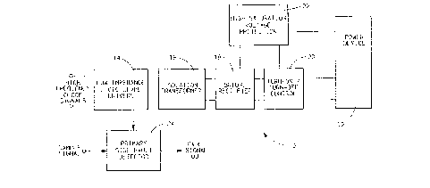
srief Description of the Drawings
Fig. 1 i5 a block diilgram of ~he primary ~ide
fault detection apparatus.
Fig. 2 is circuit di,3gram of the fault
detection apparatus ~hown in Fig. 1.
Detailed Desc~iption of the Invention
Referring to FIG. 1, circuit 10 is employed to
bias a high power device 12, such as an insulated gate
bipolar transistor ~IGBT) or a power MOSFET, conductive
and nonconductive. Power device 12 may be used in a
variety of applications which require switching devices
capable of withstanding significant voltages. Such a
power device i~ particularly well suited to use as a
switching element in a high voltage bridge inverter
application.
In circuit lO, a control signal is generated
by a controller (not shown) to bias power device 12
conductive. As embodied here, this control signal
con~ists o~ a pair of high frequency (on the order of
500 kHz to 700 k~Iz) square wave clock signals which
operate lBO degrees out of phase. The clock signals
drive lo~ impedance logic level drivers 14 whose output
creates an alternating curren~ (AC) signal at the
primary coil of one-to-one isolation transformer 16.
The secondary coil of isolation transformer 16 drives
the inputs of bridge rectifier 18 which demodulates the
AC signal into a direct current (DC) signal. The DC
signal is applied to the gate te ; n~ 1 of power device
12 to bias it conductive and enable conduction of load
curren~ bet~een the current carrying ~e inAls of power
dovice 12. Because of the inherent gate-to-source
2 ~ 7 ~ ~ ~3 ~3
capacitance of a power semicollductor, it i8 necessary
to control the rate at which t:he gate tç i n~ 1 of power
device 12 energizes and de-energizes. Turn-on/turn-off
control circuit 20 enables control of the energization
and de-energization rates, to be further described with
reference ~o FIG. 2.
When the DC signal is applied ~o the gate
t~ i n~ 1 of power device 12, high saturation voltage
protection circuit 22 compares the voltage across the
current carrying tel inA1s to a threshold voltage to
determi~e if an overvoltage or overcurrent condition
exists. Upon such a condition, the gate t~ i n~ 1 of
power device 12 i~ shunted to the source te i n~ 1 .
Shunting inhibit~ biasing power device 12 conductive,
thus preventing damage to -the device when an
overvoltage or overcurrent condition exists. As to be
further described with reference to FIG. 2, when ~he
gate and source te inals of po~er device 12 are
shunted, a low resistance path that includes the
secondary coil of isolation transformer 16 is created
in the drive circuit. This results in an increase in
current conduction in the secondary coil of isolation
transformer 16. The rise in current lavel also appears
at the primary coil of isolation transformer 16 and the
output of logic level drivers 14. The primary ~ide
fault detector 24 senses the corresponding voltage rise
at the output of logic level drivers 14 to determine
that a fault has occurred.
Primary sid~ fault detector 24 senses the
voltage at the output of lo~ic level drivers 14, as
described above. A sample signal gates the voltage at
the output of logic level drivers 14 into a circuit
2 ~ a
which holds that voltage for comparison to a
predete ined voltage. When the sampled voltage
exceeds a predete ;ned threshold, a fault signal is
activated and relayed to the system controller.
Referring to FIG. 2 and to the particulars of
circuit 10 carrying out the functions as described in
FI~. 1, a circuit diagram of the fault detection
apparatus is shown. A low level, square wave signal
(~ATECLK) is applied to logic driver 26, and a second
low level square wave signal (NOTGATECLK~, 180 degrees
out of phase irom the G~ECLK signal, i~ applied to
logic driver 28. Logic drivers 26 and 28 are low
impedance drivers capable of operating at high
frequencies. The output of logic drivers 26 and 28 is
applied to prima~y coil 30 of isolation transformer 16
to create an AC signal which drives isolation
transformer 16.
Secondary coil 32 of isolation transformer 16
drives the inputs of brid~e rectifier 18, comprised of
Schottky diodes 34, which demodulates the AC signal
into a DC signal. ThP voltage level at nod~ 36 is the
high voltage reference for power device 12,
turn-on/turn-off circuit 20 and high saturation voltage
protection circuit 2Z. Capacitor 38 is a filter
capacitor to eli in~te voltage spikes. The DC signal
provides power to the gate te i n~ 1 of power device 12,
turn-on/turn-off control circuit 20 and the high
saturation protection circuit 22. It should be noted
that with respect to yround ~ymbols as d~picted in the
FIG. 2, there e~ists a logic ground that i~ the ground
reference for the low impedance logic level drivers 14
and the primary side fault detector ~4. On the
2~7~,g
secondary side of isolation transformer 16 is a local
~round that i~ a common connection for power device 12,
turn-on/turn-off control circuit ~0, and high
saturation voltage protection circuit 22.
When GATECLK and NOTGATECLK signals are
applied, charge control circui.t 20 is activated, and
ro~istor 40 form~ an RC ~ircuit with t~e relatively
high inherent gate-to-source capacitance of power
device 12, depicted as gate capacitor 42. A~ gate
capacitor 42 charges, the gate-source voltage rises,
and power device 12 is biased conductive, allowing load
current to flow be~ween the current carrying teL ; n~ls.
To bias power device 12 nonconductive, GATECLK and
NOTGATECLK are no longex applied to drivers 26 and 28.
Thus, no DC voltage is applied to the ~urn-on/turn-o~f
control circuit 20 or the gate ter~in~l of power device
12. The voltage drop at the gate te i n~l will cause
power device 12 to bias nonconductive. In such a case,
because of the high inherent gate capacitance 4~, it i8
necessary to provide a means to control the rate of
de-energization of the gate te i n~ 1 of power device
12. Accordingly, gate capacitor 42 discharges through
resistors 40 and 44, raising the base-emitter voltag~
of tr~nsistor 4~, biasing transistor 46 conductive.
Biasing transistor 46 condllctive ~nables current
conduction through charge con~rol resistor 48, ~he
collector-emitter circuit of transistor 46, and
Schottky diode 50. Resistor 48 thus foxms an RC
circuit with gate capacitance 42 to control the rate of
discharge o~ the gate voltage. Schottky diode 50
enables transistor 46 to bias conductive because it
open circuits the path of the gate capacitance
discharge current ~etween resistor 44 and local ground,
maint~;ning the base voltage .sufficiently higher than
the emitter voltage.
Returning to the activation of the power
device, once power device 12 :is biased conductive, the
high saturation voltage pxotection circuit 22
det~ ines if power device 12 has failed to turn on or
if an overcurrent condition has occurred. Under normal
operation when power device 1:2 is initially biased
con~uctive, the voltage difference between the current
carrying t~ in~ls may be substan~ial/ as one t~ in
is often connected to a negative or positive voltage
rail, while the other terminal is at an intermediate
voltage. If voltage protection circuit 22 immediately
measured the voltage between the current carrying
terminals, a fault condition could be falsely detected
because the voltage between the t~ i n~ ls could be
significant. After a time delay, if there is no fault
upon activation of power device 12, the voltage
difference between the current carrying t~ in~ls will
be on the order of a transistor saturation voltage drop
across a power semiconductor device. The time delay
allows sufficient time for conduction of current
between the current carrying tel i n~ 1 S SO tha~ the
voltage across the current carrying te lnAI~ of power
device 12 substalltially approaches its saturation
value.
The DC signal activates delay comparator 52
which enables the time delay before activation of
comparator 54, which will compare a reference voltage
to the drain-source voltage across power device 12.
Resistor 55 and capacitor 56 form an RC circuit to
2 ~ 5
effectuate a delay in the rise time of the voltage
applied to the non-inverting .input of delay comparatox
52. The reference voltage applied to the inverting
t~ i n~ 1 of delay compara-tor l52 is derived by the
divider action of re~i~tors $8 and 60. By pxoper
selection of resistor~ 55, 58, and 60 and capacitor 56,
a sufficient time interval is introduced to delay
activation of comparator 54.
Resi~tors 62 and 64 provide a reference
voltage to the i.nvertirlg input of comparator 54 through
divider action. The voltage applied to the
non-inverting input of comparator 54 i5 controlled by
delay comparator 52. When GATECLK and NOTGA~ECLK ar8
initially applied to bias power device 12 conductive,
the output of delay comparator 52 is substantially
equal to the local ground voltage. The output of delay
comparator 52 will clamp the the non-invexting input
voltage of comparator 54 to a value less than the
inverting input voltage of comparator 54. This
maintains the output of comparator 54 low, biasing
transistor 70 nonconductive, and enables application of
the gate signal to power device 12, biasing the device
conductive.
Following the induced time delay, the voltage
to the non-invsrting input of delay comparator 5Z rises
above the reference voltage. The output of comparator
52 rises through pull-up resistor 68, causing the
voltage at the non-inverting input of comparator 54 to
rise to the equivalent of the sum of the voltage drops
across diode 72 and the current carrying te ; n~l S of
~ power device 12. Under normal operating conditions,
the sum of these voltages is less than the reference
voltage to comparator 54, and the output of the
compara~or 54 l ~in.~ low. The gate of transistor 70
is clamped to local ground, biasing it nonconductive
and enabling the DC signal to bias power device 12
conductive. If there i~ a fault condition, ~uch as
power device 12 fail~ to turn on or a high load current
exists between the current ca~rying te in~ls~ the
voltage at the non-inverting input to comparator 54
will rise, causing the output of comparator 54 to rise,
biasing txansistor 70 conductive through pull-up
resistor 71. The gate te_ i n~ 1 of power device 12 i5
shunted to local ground, preventing power device 12
from biasing conductive and conducting load current.
If the gate ter~i n~l from power device 12 is
shunted to local ground, a low resiskance path is
created from secondary coil 32 through resistor 40 and
tran~istor 70, causing a high current to flow through
secondary coil 32. By transformer action, the high
current also flows through primary coil 30 of isolation
transformer 16. The primary coil high current
condition raises the voltage at the outputs of logic
drivers 26 and 28 ~hich primary side fault detector 24
detects to determine if a fault condition has occurred.
To detect this high current condition, the voltage at
one of the the outputs of low impedance logic level
driver 26 or 28 is sampled using sample and hold
register 74. The signal S~MPLE gates the voltage into
sample and hold register 74. This voltage is output
through resistor 76, filtered by capacitor 78, to the
inverting input of fault comparator 80. ~o the
non-inverting input of fault comparator 80 is applied a
reference voltage det~ ined by a voltage divider
2 ~
compxised of resistors 82 and 84. The output of fault
comparator 80, FAULT, signals the controller that an
error has occurred. When the primary side voltage i8
below a threshold lavel, there i5 no fault condition,
and the FAULT signal L~ 9i n~ high via pull up xe3istor
86. When the primary side voltage exceed~ the
threshold levell there is a fault, and the output of
fault comparator 80 drops, causing FAUI-tr to ~o low~
A~ indicated above, this method of fault
detection enables ~ault detection without the need for
an additional tran~former. The cost and complexity of
the circuit required to isolate high power and low
power circui~s and al~o provide adequate fault
detection is thus greatly reduced.
While this invention has been described in
reference to the illustrated embodiment, it will be
understood that the scope of the present invention is
not limited thereto. Various modifications to the
illustrated embodiment may occur ~o those skilled in
the art, and it should be understood that systems
incorporating such modifications may al o fall within
the scope of this invention, which is defined by the
appended claims.