Language selection

Search

Patent 2071583 Summary

Third-party information liability

Some of the information on this Web page has been provided by external sources. The Government of Canada is not responsible for the accuracy, reliability or currency of the information supplied by external sources. Users wishing to rely upon this information should consult directly with the source of the information. Content provided by external sources is not subject to official languages, privacy and accessibility requirements.

Claims and Abstract availability

Any discrepancies in the text and image of the Claims and Abstract are due to differing posting times. Text of the Claims and Abstract are posted:

  • At the time the application is open to public inspection;
  • At the time of issue of the patent (grant).
(12) Patent: (11) CA 2071583
(54) English Title: SYSTEM FOR CONVERTING SYNCHRONOUS TIME-DIVISION SIGNALS INTO ASYNCHRONOUS TIME-DIVISION DATA PACKETS
(54) French Title: SYSTEME DE CONVERSION DE SIGNAUX SYNCHRONES A MULTIPLEXAGE TEMPOREL EN PAQUETS DE DONNEES ASYNCHRONES A MULTIPLEXAGE TEMPOREL
Status: Expired and beyond the Period of Reversal
Bibliographic Data
(51) International Patent Classification (IPC):
  • H04J 3/16 (2006.01)
  • H04J 3/26 (2006.01)
  • H04Q 11/04 (2006.01)
(72) Inventors :
  • VAN DER VEEN, HENDRIK
(73) Owners :
  • KONINKLIJKE PHILIPS ELECTRONICS N.V.
  • N.V. PHILIPS' GLOEILAMPENFABRIEKEN
(71) Applicants :
  • KONINKLIJKE PHILIPS ELECTRONICS N.V.
  • N.V. PHILIPS' GLOEILAMPENFABRIEKEN
(74) Agent: SMART & BIGGAR LP
(74) Associate agent:
(45) Issued: 2003-06-03
(22) Filed Date: 1992-06-18
(41) Open to Public Inspection: 1992-12-22
Examination requested: 1999-06-15
Availability of licence: N/A
Dedicated to the Public: N/A
(25) Language of filing: English

Patent Cooperation Treaty (PCT): No

(30) Application Priority Data:
Application No. Country/Territory Date
91201596.3 (European Patent Office (EPO)) 1991-06-21

Abstracts

English Abstract


System for converting synchronous time-division (STD) signals into
asynchronous data packets (ATD), in which the incoming and outgoing signals
are
spread over various (multiplex) channels. Not more than a single RAM and a
single
FIFO are utilized for various channels together. The RAM is subdivided into
rows and
columns, one column per channel, data packets being preferably stored in
successive
columns shifted by at least 1 row.


Claims

Note: Claims are shown in the official language in which they were submitted.

5
CLAIMS:
1. ~A system for converting a synchronous time-
division signal into an asynchronous time-division data
packet, comprising:
first storage means having an input for receiving
the synchronous time-division signal, said first storage
means further having an output, wherein said first storage
means is a random access memory divided into columns and
rows, wherein each column of the random access memory
corresponds to an asynchronous time-division data packet and
each row of the column corresponds to a byte of the
asynchronous time-division data packet;
second storage means having an input for receiving
the synchronous time-division signal from said first storage
means, said second storage means further having an output;
and
control means for sending an address signal to
said second storage means for converting the synchronous
time-division signal into the asynchronous time-division
data packet, wherein the synchronous time-division signal is
transmitted from the random access memory to said second
storage means when a predetermined number of rows in a
column of the random access memory have received the time-
division signal.
2. ~The system as claimed in claim 1, wherein the
address signal is a header and wherein said control means
transmits the header to said second storage means.
3. ~The system as claimed in claim 1, wherein the
address signal is a packet header and wherein said control
means transmits the packet header to said second storage

6
means, the packet header being combined with the synchronous
time-division signal in said second storage means to form
the asynchronous time-division data packet.
4. The system as claimed in claim 2, wherein said
second storage means is a first-in first-out memory.

Description

Note: Descriptions are shown in the official language in which they were submitted.


CA 02071583 2002-11-O1
20104-8745
1
System for converting synchronous time-division signals into
asynchronous time-division data packets.
The invention relates to a system for processing
synchronous time-division (STD) signals as well as
asynchronous time-division (ATD) data packets, in which
input signals spread over various input channels are
converted into output signals spread over various output
channels, in response to control means the input signals
being temporarily stored in a first-in first-out (FIFO)
memory and read out therefrom, and are also temporarily
stored in a RAM and read out therefrom as well.
A similar system in known from United States
Patent 4,612,636. In the system described in that Patent
asynchronous data packets comprising each a header with a
channel address for which the packet information is
intended, as well as two information bytes, are stored in a
FIFO (first-in first-out buffer). The header of the
asynchronous data packets determines a memory location in a
RAM at which the information bytes are then stored. Each
memory location is coupled to a specific output channel.
The RAM memory locations associated to an output channel
(for example, a time channel in a multiplex signal) are read
out cyclically, so that the information concerned appears on
an output line as a signal, possibly in multiplex form,
synchronized with other channels. The asynchronous data
packets applied to the system are also spread over various
channels (possibly multiplex channels). The use of a FIFO
in combination with a RAM avoids that a FIFO and a control
is necessary for each channel.
A drawback of the prior-art system is that it is
only suitable for converting asynchronous data packets into

CA 02071583 2002-11-O1
20104-8745
la
synchronous multiplex signals, whereas there is also a need
for a system converting synchronous time-division signals
into asynchronous time-division data packets.
It is an object of the invention to adapt the
prior-art system, so that a system is developed converting
synchronous time-division signals into asynchronous time-
division data packets.
The present invention provides a system for
converting a synchronous time-division signal into an
asynchronous time-division data packet, comprising: first
storage means having an input for receiving the synchronous
time-division signal, said first storage means further
having an output, wherein said first storage means is a
random access memory divided into columns and rows, wherein
each column of the random access memory corresponds to an
asynchronous time-division data packet and each row of the
column corresponds to a byte of the asynchronous time-
division data packet; second storage means having an input
for receiving the synchronous time-division signal from said
first storage means, said second storage means further
having an output; and control means for sending an address
signal to said second storage means for converting the
synchronous time-division signal into the asynchronous time-
division data packet, wherein the synchronous time-division
signal is transmitted from the random access memory to said
second storage means when a predetermined number of rows in
a column of the random access memory have received the time-
division signal.
The system according to the invention is thereto
characterized, in that the input signals are the STD
signals, the output signals are the ATD packets and the STD

2t9'~~.~8~
PHN 13.750 2 04.06.1992
signals are first stored in the RAM before being placed in the FIFO.
With these measures the state-of the-art problems are avoided.
This provides an optimum time-division packet handling with minimum
hardware.
The invention will be further explained with reference to a drawing
Figure which is merely intended to be used for illustrative purposes and is
not to be
regarded as a restriction, in which:
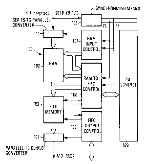
Fig. 1 shows a system for converting time-division synchronous signals
into asynchronous time-division data packets and
Fig. 2 shows a memory layout of the RAM in the system shown in Fig.
1.
Fig. 1 shows a system 100 for converting a synchronous time-division
signal referenced STD signal (Synchronous Time-Division), into an asynchronous
data
packet referenced ATD packet (Asynchronous Time-Division).
The incoming STD signal is transported to a RAM 102 in response to a
RAM input control 107 through a series-to-parallel converter 101. If the
latter is not
explicitly included, synchronizing means 10$ derive time synchronizing
information
from the incoming channels. The series-to-parallel converter 101 has for its
function to
carry out the data processing at a lower rate. Various input channels, for
example, in
the form of multiplex time-division channels, can be connected to the system
shown in
Fig. 1. The RAM 102 has such a memory structure that a column is reserved for
each
incoming channel, with each column comprising a number of rows for individual
ir_formation packets.
In response to a RAM-to-FIFO control 106 the information is taken from
the columns of the RAM 102 to a FIFO memory 103 (First In First Out), where a
header identifying the destination of the data packet is affixed to the data
packet. The
FIFO 103 has an independent access for read and write operations and is used
for the
desired rate adjustments. The RAM input control 10'7 knows about the
organization of
the input channels, for example, 32 channels of 64 kbitls and, on the basis
thereof, fills
the RAM memory locations. This should be effected in such a way that the
complete
data packets for the different output channels are finished is effected in a
time-division
mode. In that case the data transfer control is loaded as uniformly as
possible and the
formation of data packets for the different output channels is delayed the
least possible.

PHN 13.750 3 04.06.1992
The RAM-to-F1F0 control 106 comprises, for example, a Table of
headings for each column in the RAM. The headings Table itself is controlled
by a PD
control 109 which includes an error detection section. The header comprises,
for
example, a transfer bit denoting whether a specific output channel is to be
supplied with
a data packet. The RAM-to-FIFO control 106 continuously scans the rows in the
RAM
102. If a sufficient number of rows in a column are filled for assembling a
data packet,
the RAM-to-FIFO control 106 places a header in the FIFO 103 and adds in the
fastest
way possible the relevant contents of the column to the header, unless the
transfer bit of
the header has a zero value. Subsequent to the transfer to the FIFO 103, a
signal is sent
to a FIFO output control 105, which in its turn transfers the data packets
located in the
FIFO 103 to the ATD output channels while maintaining the desired
synchronization.
In the present system the manner in which the RAM 102 is arranged is
of importance. Each column comprises as .many rows as is strictly necessary
for storing
a data packet. In the case where a data packet comprises N bytes, each column
in the
RAM comprises exactly N-byte memory locations. If the write pointer, whose
position
is generated by the RAM input control 107, is at the end of these N memory
locations,
a data packet is full. The RAM-FIFO control 106 then receives from the RAM
input
control 107 the associated column address for addressing the desired output
channel,
and transfers the data packet concerned to the FIFO 103. This transfer is to
be effected
as soon as possible, but is to be completed before the next information byte
for the
associated column arrives.
Fig. 2 shows, for example, that packet (x+1) of column 4 is full (the
write pointer has a value N). This packet is to be transported to the FIFO
before the
arrival of the next information byte for column 4.
It should be observed that the previously terminated packet was packet
(x+2) of column 5 and, therefore, the reading of the packet from this column 5
had
certainly been terminated before said next information byte for column 4
arrived.
The information from this column has thus already been transported to
the FIFO and the first byte of the new packet can be written in the zero' row.
In an extremely advantageous embodiment of the invention the
synchronous signals are shifted per column row (e.g. 1 row) in the memory
matrix of
rows and columns as is shown in Fig. 2. If in the first column C1, for
example, the
filling of a data packet is commenced in the zeros row 1t0, this is commenced
in the i~'

2~'~~58~
PHN 13.750 4 Od.06.1992
column C1 on the (i-1)st row R(i-1). The row-shifted data packet storage in
the RAM
ensures that the data packets become available efficiently divided over time.
An
extremely efficient data packet transfer to the FIFO may therefore be
effected. A
minimum-size FIFO may also suffice, because the transfer is effected uniformly
divided
over time. Each filled data packet will be presented to the FIFO with the same
(minimum) time delay.

Representative Drawing
A single figure which represents the drawing illustrating the invention.
Administrative Status

2024-08-01:As part of the Next Generation Patents (NGP) transition, the Canadian Patents Database (CPD) now contains a more detailed Event History, which replicates the Event Log of our new back-office solution.

Please note that "Inactive:" events refers to events no longer in use in our new back-office solution.

For a clearer understanding of the status of the application/patent presented on this page, the site Disclaimer , as well as the definitions for Patent , Event History , Maintenance Fee  and Payment History  should be consulted.

Event History

Description Date
Inactive: IPC expired 2013-01-01
Inactive: IPC from MCD 2006-03-11
Time Limit for Reversal Expired 2005-06-20
Letter Sent 2004-06-18
Grant by Issuance 2003-06-03
Inactive: Cover page published 2003-06-02
Pre-grant 2003-03-12
Inactive: Final fee received 2003-03-12
Notice of Allowance is Issued 2003-01-22
Letter Sent 2003-01-22
Inactive: Approved for allowance (AFA) 2003-01-02
Amendment Received - Voluntary Amendment 2002-11-01
Inactive: S.30(2) Rules - Examiner requisition 2002-08-27
Amendment Received - Voluntary Amendment 1999-07-09
Inactive: Application prosecuted on TS as of Log entry date 1999-06-29
Letter Sent 1999-06-29
Inactive: Status info is complete as of Log entry date 1999-06-29
Request for Examination Requirements Determined Compliant 1999-06-15
All Requirements for Examination Determined Compliant 1999-06-15
Application Published (Open to Public Inspection) 1992-12-22

Abandonment History

There is no abandonment history.

Maintenance Fee

The last payment was received on 2002-03-20

Note : If the full payment has not been received on or before the date indicated, a further fee may be required which may be one of the following

  • the reinstatement fee;
  • the late payment fee; or
  • additional fee to reverse deemed expiry.

Please refer to the CIPO Patent Fees web page to see all current fee amounts.

Fee History

Fee Type Anniversary Year Due Date Paid Date
MF (application, 6th anniv.) - standard 06 1998-06-18 1998-03-25
Registration of a document 1998-08-05
MF (application, 7th anniv.) - standard 07 1999-06-18 1999-03-23
Request for examination - standard 1999-06-15
MF (application, 8th anniv.) - standard 08 2000-06-19 2000-03-08
MF (application, 9th anniv.) - standard 09 2001-06-18 2001-03-19
MF (application, 10th anniv.) - standard 10 2002-06-18 2002-03-20
Final fee - standard 2003-03-12
MF (patent, 11th anniv.) - standard 2003-06-18 2003-05-26
Owners on Record

Note: Records showing the ownership history in alphabetical order.

Current Owners on Record
KONINKLIJKE PHILIPS ELECTRONICS N.V.
N.V. PHILIPS' GLOEILAMPENFABRIEKEN
Past Owners on Record
HENDRIK VAN DER VEEN
Past Owners that do not appear in the "Owners on Record" listing will appear in other documentation within the application.
Documents

To view selected files, please enter reCAPTCHA code :


To view images, click a link in the Document Description column. To download the documents, select one or more checkboxes in the first column and then click the "Download Selected in PDF format (Zip Archive)" or the "Download Selected as Single PDF" button.

List of published and non-published patent-specific documents on the CPD .

If you have any difficulty accessing content, you can call the Client Service Centre at 1-866-997-1936 or send them an e-mail at CIPO Client Service Centre.


Document
Description 
Date
(yyyy-mm-dd) 
Number of pages   Size of Image (KB) 
Representative drawing 2003-04-29 1 9
Cover Page 2003-04-29 1 37
Representative drawing 2002-08-21 1 7
Description 2002-11-01 5 194
Claims 2002-11-01 2 52
Drawings 2002-11-01 1 19
Claims 1993-12-18 1 27
Drawings 1993-12-18 1 14
Abstract 1993-12-18 1 12
Description 1993-12-18 4 146
Cover Page 1993-12-18 1 14
Reminder - Request for Examination 1999-02-22 1 116
Acknowledgement of Request for Examination 1999-06-29 1 179
Commissioner's Notice - Application Found Allowable 2003-01-22 1 160
Maintenance Fee Notice 2004-08-16 1 172
Correspondence 2003-03-12 1 36
Fees 1997-03-20 1 81
Fees 1996-03-21 1 67
Fees 1995-03-08 1 76
Fees 1994-03-23 1 59