Note: Descriptions are shown in the official language in which they were submitted.
2012112
SPECIFICATION
COLOR FILTERS, THEIR PRODUCTION PROCESS, COLOR
LIQUID CRYSTAL PANELS AND METHOD OF DRIVING THE PANELS
TECHNICAL FILED
The present invention relates to a color filter and a
process for producing a color filter. The present invention
further relates to a color liquid crystal panel comprising the
color filter and a method of driving the color liquid crystal
panel.
BACKGROUND ART
Color filters prepared by laminating a coloring matter
layer on an insulating substrate are used in a color liquid
crystal panel for a display of a liquid crystal TV, a personal
computer or the like. Heretofore, color filters having a
structure as indicated in Fig. 16, have been known. In the color
filter as indicated in Fig. 16, a transparent ITO (Id-Sn oxide)
electrode (b) is formed on an insulating glass substrate (a). On
the ITO electrode, coloring matter layers (c) for primary three
colors, i.e., R (red), G (green) and B (blue), are formed, and a
black matrix (light-shielding film) (d) is formed between each of
the coloring matter layers (C). Such black matrix is used to
avoid lowering of contrast and color purity due to leaked light.
In addition, in Fig. 16, (e) denotes a top coating layer and (f)
denotes a post-ITO layer.
In general, the coloring matter layers of the color
filters are formed by known methods. Such known methods include:
a printing method which comprises printing inks for three primary
colors (RGB) on a glass substrate with use of a printing
equipment; a dispersion method which comprises applying a pigment
dispersed in a UV-curable resist on a glass substrate, and then
- 1 -
20721 l 2
forming coloring matter layers for red, green and blue by
repeating mask exposure and thermal curing, three times, by way
of a photo-lithography method; a dyeing method which comprises
forming a resist layer as a dye preventing layer on a gelatin
layer, and dyeing the gelatin layer to form coloring matter
layers for RGB; an electro-deposition method which comprises
forming a dispersion of a pigment and an electrodepositing
polymer, and subjecting the dispersion to electro-deposition
treatment utilizing an electrode formed on the substrate; and a
micellar disruption method which comprises forming a dispersion
of a pigment and a surfactant, and subjecting the dispersion to
electrolytic treatment utilizing an electrode formed on the
substrate.
The coloring matter layers of the color filter as shown
in Fig. 16 are usually formed by way of an electrical treatment
such as an electro-deposition method or a micellar disruption
method (Refer to Japanese Patent Application Unexamined
Publication No. 63-243298).
Carbon type photo-resist materials are widely used in
the other color filter production methods such as a printing
method, dispersion method and dyeing method. However, if such
carbon type photo-resist materials are used in the electrical
treatment such as a micellar disruption method or an
electro-deposition method, there will be several problems due to
their conductivity. More specifically, if such a conductive
resist material is used, when a black matrix is first formed and
then coloring matter layers are formed, or when electrodes for
forming coloring matter layers are used to drive liquid crystals,
the vicinal transparent electrodes will be electrically connected
through the black matrix. Thus, the operations cannot be
properly conducted.
Accordingly, in a micellar disruption method or an
electro-deposition method, as an insulating resist material used
- 2 -
2072112
for forming a black matrix, insulating ones preferably having a
surface resistance of not less than 10~ S2/cm2 are used.
As insulating resist material used for forming a black
matrix, organic pigment type materials are known.
However, when a black matrix is prepared from an
organic pigment type insulating resist material, there is a
problem that the light-shielding rate is decreased. This is
because a black matrix is formed by way of a photo-lithography
method using a blend of three kinds of a resist material each
containing a pigment for red, green or blue.
It is said that as for the light-shielding rate, for
example, in the case of a TFT panel, optical density (OD) should
be as high as 3.5 or more. However, in the case of an organic
pigment type resist material, it is difficult to prepare a black
matrix having an OD of at least 2.5.
It is desired that a metal black matrix is used as a
black matrix having high light-shielding rate. However, in the
case of using the metal black matrix in a micellar disruption
method or an electro-deposition method, there will be the problem
as is the same case with the above-mentioned carbon type resist
due to conductivity of the metal black matrix. In other words,
the micellar disruption method and the electro-deposition method
cannot be used to form a coloring matter film. Also, a
transparent electrode for forming a coloring matter film cannot
be used to drive a liquid crystal.
Accordingly the first invention has its object to
provide a color filter and its production process which solve the
above-mentioned problems, i.e., having a structure wherein the
vicinal transparent electrodes are not electrically connected
even when a metal black matrix is used.
Further, the first invention has another object to
provide a color liquid crystal panel and its driving method.
In the meanwhile, a printing method, a dispersion
method and a dyeing method can form a coloring matter layer in a
- 3 -
2072112
desired place on a glass substrate (e. g., effective display
portion) because of their nature in the production process.
However, when a color filter is formed by a micellar disruption
method, an electro-deposition method or the like using
electricity passing treatment as used in the first invention, the
following procedure is needed. As shown in Fig. 17, it is
necessary to form an electrode 6a for electricity passing
treatment by taking out an electrode in a portion other than an
effective display area S (non-effective display area) in order to
connect a coloring matter layer forming transparent electrode 6
in the effective display area S to an outer electrode.
Further, as shown in Figs. 17 and 18, it is required
that the electricity passing treatment should be conducted for an
electrode for the same color, at the same time, among
stripe-shaped transparent electrodes for forming coloring matter
layers arranged in the order of red, green and blue. To do this,
the electrodes 6a for the electricity passing treatment for RGB
should be formed such that each electrode 6a for each color
should have different length; an insulating film is formed on an
electrode taking out window frame 13; an electrode taking out
window 14 is formed in the insulating film; then a silver paste
15 is applied along with the window for each color in the
stripe-shape. Thus, the contact of the electrodes for each color
is made.
Further, the present applicant provided in an earlier
patent application (Japanese Patent Application No. 241084/89), a
technique to simplify these steps. In such technique, when a
black matrix is formed using a light-shielding resist, an
electrode taking out window is formed using said resist.
However, in the above-mentioned conventional production
process for producing a color filter, there is a problem that a
step of applying a silver paste along with the electrode taking
out window in the stripe-shape is required.
- 4 -
2072112
Further, when a liquid crystal display is assembled
(cell assembling) using a color filter, a step of removing the
silver paste or a step of cutting or scrubbing the silver paste
portion using a dicer or scrubber, is required.
Furthermore, there is a problem that additional
equipments are required to remove dusts made at the time of
removing the silver paste by vacuum treatment or the like.
Accordingly, the second invention has its object to
provide a color filter, its production process, a color liquid
crystal panel and its driving method, which can omit silver paste
applying/removing steps, resulting in improvement of
productivity.
DISCLOSURE OF THE INVENTION
The color filter according to the first embodiment of
the present invention is prepared by laminating a metal black
matrix, an insulating film, a transparent electrode and a
coloring matter layer, in this order, on one side of an
insulating substrate.
In the color filter of the first embodiment, the
vicinal transparent electrodes are not electrically connected
since there is an insulating layer between the metal black matrix
and the transparent electrodes. Further, use of the metal black
matrix results in high light-shielding rate (usually OD is at
least 3.5) and good contrast. Thus, the color filter can be
suitably used as a color filter for an active matrix such as TFT
or MIM. Further, since the coloring matter layers and the metal
black matrix are electrically disconnected by the insulating
layer, the electrodes for forming a coloring matter layer can be
used as electrodes for driving a liquid crystal.
Further, a process for producing a color filter
according to the fist embodiment of the present invention
comprises the following steps (1) to (6):
- 5 -
2072112
(1) a step of laminating a metal thin film used for
forming a black matrix on one side of an insulating
substrate;
(2) a step of subjecting the above metal thin film to
patterning treatment to form a black matrix;
(3) a step of laminating an insulating film by covering the
above metal black matrix;
(4) a step of laminating a transparent electrode forming
material on the above insulating film;
(5) a step of subjecting the above transparent electrode
forming material to patterning treatment to form a
transparent electrode; and
(6) a step of laminating a coloring matter layer on the
above transparent electrode by way of a coloring matter
film forming method using an electricity passing
treatment.
According to the process of the first invention, a
coloring matter layer can be formed by a method using electricity
passing treatment such as a micellar disruption method or an
electro-deposition method since the transparent electrodes are
not connected to each other. Thus, in addition to the effect of
the metal black matrix, a stable color filter having a high
light-shielding property, good surface flatness and high color
purity, and not showing delamination and non-uniform color, can
be produced. Further, according to the process of the first
invention, soda lime glass which has not been subjected to
polishing, silica coating or the like can be used as an
insulating substrate.
Further, a method of driving the color liquid crystal
panel according to the first invention comprises driving the
color liquid crystal panel with use of transparent electrodes for
forming a coloring matter layer.
- 6 -
2072112
Further, the color filter according to the second
invention is prepared by laminating, in this order, a black
matrix and a taking out electrode, an insulating film having a
window for a taking out electrode, a transparent electrode for
forming a coloring matter layer, an insulating protection layer,
a coloring matter layer, a flattening film and an electrode for
driving a liquid crystal on an insulating substrate,
characterized in that said taking out electrode and the
transparent electrode for forming a coloring matter layer are
electrically connected through said window for a taking out
electrode.
Furthermore, a process for producing a color filter
according to the second invention comprises: forming and
laminating, in this order, a black matrix, a taking out electrode
and an insulating film having a window for a taking out
electrode; forming a transparent electrode for forming a coloring
matter layer on the insulating layer in such manner that the
transparent electrode can be electrically connected to the taking
out electrode through the widow for a taking out electrode; and
then forming a coloring matter layer by passing electricity to
the transparent electrode for forming a coloring matter layer
through the taking out electrode. Preferably, the exposure and
development time for the photo-lithography treatment is
controlled to form the periphery portion of the taking out
electrode window of the insulating film in the taper shape.
Further, a color liquid crystal display according to
the second invention is composed of the above-mentioned color
liquid crystal panel, an electrode substrate for driving a liquid
crystal and a liquid crystal encapsulated between them.
According to the color filter and the color liquid
crystal display of the second invention, the silver paste
applying and removing steps can be omitted. Thus, the process
can be simplified.
Zo~2> > z
In addition, according to the production process of a
color filter of the second invention, the color filter according
to the second invention can be effectively produced.
BRIEF DESCRIPTION OF DRAWINGS
Fig. 1 is a cross-sectional view of one example of the
color filter according to the first invention; Fig. 2 is a
cross-sectional view of another example of the color filter
according to the first invention; Fig. 3 is a plan view showing a
mask for forming a transparent electrode; Fig. 4 is a plan view
showing a mask for forming a black matrix and an electrode taking
out zone; Figs. 5 and 6 are cross-sectional views of an electrode
taking out zone; Fig. 7 shows a structure of the color filter
according to the second invention; Fig. 8 is a partially
cross-sectional view showing a structure of the color filter
according to the present invention; Fig. 9 shows steps of a
process for producing the color filter according to one example
of the second invention; Figs. 10 and 11 are plan views showing a
mask used in the steps as shown in Fig. 9; Fig. 12 is a
cross-sectional view showing a situation wherein the electrode
taking out window is formed in the taper shape; Fig. 13 shows
another mask used in the steps as shown in Fig. 9; Fig. 14 is a
cross-sectional view of a color liquid crystal display; Fig. 15
shows steps of a process for assembling a color liquid crystal
display; Fig. 16 is a cross-sectional view showing a structure of
a conventional color filter; Fig. 17 is a plan view showing a
structure of a conventional color filter; and Fig. 18 is a
cross-sectional view showing a structure of a conventional color
filter.
MOST PREFERRED EMBODIMENTS CARRYING OUT THE INVENTION
The first invention will be described in more detail
with reference to the attached drawings.
_ g _
-2072112
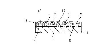
Fig. 1 shows one example of a color filter according to
the first invention. The color filter is made useful for driving
MIM or STN.
In the color filter, 1 denotes an insulating substrate.
A metal black matrix 2 which has been subjected to patterning is
formed on one side of the substrate 1, and an insulating film 4
is laminated to cover the black matrix. Further, transparent
electrodes 6 which have been subjected to patterning, are formed
on the insulating layer 4. Coloring matter layers 8 for RGB
primary colors are formed on the transparent electrodes 6.
Further, a top coating layer 11 is laminated on the coloring
matter layers 8. Post-ITO layer 12 which has not been subjected
to patterning, is formed on the top coating layer 11.
Fig. 2 shows another example of the color filter
according to the first invention. The color filter is made
useful for driving TFT. In the color filter, an insulating
substrate 1, a metal black matrix 2, an insulating film 4,
transparent electrodes 6 and coloring matter layers 8 are the
same as those in Fig. 1. In this example, a top coating layer is
not formed, and a post-ITO layer 12 which has not been subjected
to patterning is laminated on the coloring matter layers 8. Of
course, a top coating layer can be formed.
In addition, the above-mentioned color filter is used
for driving MIM, STN or TFT. However, it is possible that the
structure can be modified in several ways depending upon the
intended use or the like within the spirit of the present
invention.
Next, the process for producing a color filter of the
first invention will be explained in the order of the steps (1)
to (6).
(1) A thin metal film used for forming a black matrix
is laminated on one side of an insulating substrate.
In this case, as an insulating substrate, a glass
substrates such as soda lime glass, non-alkali glass can be
_ g _
.l"~.i
2012112
preferably used. In addition, as soda lime glass, non-polished
products as well as polished products can be used. More
specifically, recently a soda lime glass substrate is usually
subjected to polishing treatment (mirror polishing) if used as a
liquid crystal panel, because the scratches on the soda lime
glass surface cause braking of electrode lines at the time of ITO
patterning. Also, soda lime glass is usually subjected to a
silica coating treatment because the alkali elution causes
shortening of the life of the liquid crystal. On the contrary to
this, in the present invention, the treatment to the soda lime
glass (polishing, silica dipping) is not required because the
black matrix and the insulating film can avoid the alkali
elution, and flatten the surface.
Further, metals for the black matrix are not
particularly limited, but chromium or nickel is preferably used.
As a method of forming a thin metal film, sputtering,
vapor deposition, CVD or the like can be mentioned.
(2) The above-mentioned thin metal film is subjected
to patterning to form a black matrix.
In this case, patterning methods are not limited to,
but include, for example, a method comprising conducting resist
application by a roll coater or a spin coater; exposure treatment
with a stepper exposing equipment or a.one-shot exposing
equipment; development; etching; and resist removal in this
order.
(3) An insulating film is laminated to cover the
above-mentioned thin metal black matrix.
In this case, the materials for the insulating film are
not limited to, but preferably include, for example, silica,
titanic, alumina and an insulating polymer.
Examples of methods of forming the insulating film are,
for example, a method of sputtering silica, titanic or alumina, a
method of dipping in silica and a method of coating an insulating
polymer.
- 10 -
-- 20721 i 2
(4) A transparent electrode forming material is
laminated on the above-mentioned insulating film. In this case,
examples of the transparent electrode forming materials are ITO
and tin oxide. Examples of a method of laminating the
transparent electrode forming material are a sputtering method, a
vapor deposition method and a pyro-sol method.
(5) A transparent electrode is formed by subjecting
the above-mentioned transparent electrode forming material to
patterning.
In this case, examples of a method of patterning can be
the same as those previously described for the above-mentioned
step (2).
(6) A coloring matter layer is laminated on the
above-mentioned transparent electrode.
In this case, as a method of forming a coloring matter
layer, a method using electricity passing treatment, particularly
a micellar disruption method or an electro-deposition method, can
t be preferably used.
To form the above coloring matter thin film by a
micellar disruption method, the following procedures can be used.
A micelle forming agent comprising ferrocene derivatives and a
coloring matter material (hydrophobic coloring matter) are added
to an aqueous solvent having a controlled conductance prepared by
adding, as necessary, a support electrolyte to water. The
mixture is well stirred to obtain a micelle containing the
coloring matter material therein. When the micelle solution is
subjected to electrolytic treatment, the micelle moves to an
anode. The ferrocene derivative contained in the micelle loses
an electron, e- (Fe2+ of the ferrocene is oxidized to Fe3+) on
the anode (transparent electrode), and at the same time the
micelle is broken. When the micelle is broken, a coloring matter
material is precipitated on the anode to form a thin film.
On the other hand, the oxidized ferrocene derivative
moves to a cathode and receives an electron, e- to reform a
- 11 -
2072112
micelle. While the micelle formation and breakage are repeated,
coloring matter particles are precipitated on the transparent
electrode to form a thin film. The desired coloring matter thin
film is formed in this manner. The thus obtained coloring matter
thin film has, in general, a thickness of 0.1 to 10.0 um,
preferably 0.1 to 2.0 um. Due to the porous structure of the
thin film, the thin film has high conductance.
If the film thickness is less than 0.1 um, the hue of
the coloring matter layer cannot sufficiently be exhibited. If
the thickness is more than 10.0 um, the film will have low
conductance. Thus, the thin film having the above thickness
range is preferable.
In the case of forming coloring matter films for three
primary colors by the above-mentioned micellar disruption method,
any one of red, green and blue hydrophobic coloring matters is
first added to an aqueous medium, and the first desired color
thin film is formed by the above-mentioned micellar disruption
method. Then, the micelle electrolytic treatment is repeatedly
carried out using different hydrophobic coloring matter to form
coloring matter films for the three primary colors (red, green,
blue) on each transparent electrode. In addition, it is possible
to get hydrophobic coloring matters for red, green and blue
dispersed in an aqueous medium at the same time, and subject the
aqueous medium to the micelle electrolytic treatment to produce
the similar coloring matter films.
In the production process according to the present
invention, in addition to the above-mentioned steps, the
following steps (7) to (9) can be conducted.
(7) An electrode taking out zone can be formed in the
color filter by using an insulating resist material and an
electrically conductive material before or after the formation of
the coloring matter films. According to this step, a color
filter capable of using transparent electrodes for forming a
- 12 -
~0~2 » 2
coloring matter layer as electrodes for driving crystal liquids,
can be readily produced.
For example, if patterning of a transparent electrode
is conducted using a mask 100 as shown in Fig. 3 in the
above-mentioned step (5), 10 sets of three electrode lines (i.e.,
the shortest line 6B, the middle length line 6G and the longest
line 6R) can be formed. The three lines 6B, 6G and 6R correspond
to three primary colors for light, i.e., blue (B), green (G) and
red (R), respectively.
An insulating layer for taking out an electrode is
formed with an insulating resist material and a mask 101 as shown
in Fig. 4. The mask 101 has not only a black matrix pattern 2,
but also an electrode taking out zone pattern 13. The pattern 13
comprises patterns for forming three sets of electrode taking out
window belts. In other words, the pattern 13 comprises a pattern
14B for forming an electrode taking out window belt for electrode
lines (B), a pattern 14G for forming an electrode taking out
window belt for electrode lines (G) and a pattern 14R for forming
an electrode taking out window belt for electrode lines (R).
Further, electrically conductive layers for taking out electrodes
are formed by using an electrically conductive material.
Figs. 5 and 6 show an electrode taking out zone of a
color filter produced by using a mask 100 and a mask 101. Fig. 5
is a cross-sectional view of a color filter, taken along the v-V
line of a mask 101. Fig. 6 is a cross-sectional view of a color
filter, taken along the VI-VI line of a mask 101. As shown in
Figs. 5 and 6, the electrode lines 6G and 6R are coated with an
insulating layer 13. The electrode lines 6B are electrically
connected to each other through an electrically conductive layer
15.
In addition, the insulating resist materials for
forming the insulating layer usually include a negative type W
sensitive resist. The electrically conductive materials for
forming the electrically conductive layers include, for example,
- 13 -
2~72~~2
an electrically conductive thin film and electrically conductive
paste.
(8) If necessary, like the color filter as shown in
Fig. 1, a top coating material may be coated with a spin coater
or a roll coater on the coloring matter layer and dried at 80 to
150oC for 5 to 60 minutes to form a top coating layer. The top
coating material include, for example, an acrylic resin,
polyether resin, polyester resin, polyolefin resin, phosphazene
resin, or polyphenylene sulfide resin. If the coating layer is
prepared from a conductive material, voltage down due to the
coating layer can be prevented, and the electrodes for forming a
coloring matter layer can be effectively used as electrodes for
driving a liquid crystal.
(9) If necessary, like the color filter as shown in
Figs. 1 and 2, a post-ITO layer is formed on a top coating layer
(Fig. 1) or a coloring matter layer (Fig. 2). The post-ITO layer
functions as an electrode for driving a liquid crystal separately
from the electrode for forming a coloring matter layer. In
addition, in the case of producing a color filter for driving MIM
or STN, a post-ITO is subjected to patterning (Fig. 1).
The color liquid crystal panel according to the present
invention is produced using the above-mentioned color filter. In
this case, a means for producing a panel is not limited.
However, the following method can~be preferably used.
First, an orientation layer is formed by coating, for
example, a polyamic acid monomer, a polyimide resin oligomer or
the like by a spin coater or a roll coater on a color filter,
polymerizing the coated material at 200 to 300oC for 30 minutes
to 2 hours, washing with pure water or the like, and drying the
polymerized product (at 60 to 100oC for 30 minutes to 2 hours or
by IR radiation or the like). The liquid crystals can be
oriented by the orientation layer. Then, a color filter is fixed
to a driving electrode substrate such as TFT, MIM (active matrix)
and DUTY (simple matrix) using a spacer made of glass beads or
- 14 -
2072112
plastics and an encapsulating agent such as adhesive, and then
subjected to rubbing treatment such as abrasion rubbing or
oblique evaporation. Simultaneously, a liquid crystal such as
TN, STN, FLC, AFLC or VAN is pored, by vacuum poring or the like,
between the driving electrode substrate and the color filter.
According to the method of driving a color liquid
crystal panel of the present invention, a color liquid crystal
panel is driven by a transparent electrode used to form a
coloring matter layer. In this case, as a driving circuit,
desired ones such as MIM and TFT can be used depending upon the
kind of the color filter used. Further, in this case, a post-ITO
is not formed.
Next, the second invention will be described in more
detail with reference to the attached drawings.
Fig. 7 is a cross-sectional view showing a color filter
according to the present invention. Fig. 8 is a partially plan
view of the same.
In the color filter according to the second invention,
as shown in Figs. 7 and 8, a black matrix 2 and taking out
electrodes 3 are formed on an insulating substrate 1. The black
matrix 2 and the taking out electrodes 3 are composed of a
light-shielding conductive film such as chromium and nickel.
On the black matrix 2 and the taking out electrodes 3,
an insulating film 4 is formed, and a taking out electrode window
is formed in the portion of the insulating film 4, said portion
corresponding to the taking out electrodes 3.
On the insulating film 4, the transparent electrodes
for forming a coloring matter layer are formed. The transparent
electrodes 6 for forming a coloring matter layer and the taking
out electrodes 3 are electrically connected through the taking
out electrode window 5. The electrical contact can be made by
filling an electrically conductive material in the taking out
electrode window 5.
- 15 -
2072112
An insulating protection film 7 is formed on the
insulating substrate 1 having the transparent electrodes 6 for
forming a coloring matter layer thereon, provided that the
insulating protection film 7 is not formed on the portion of the
substrate corresponding to the effective display area S. The
insulating protection film 7 is formed on the substrate before
coloring matter layers are formed.
The electricity passing electrodes 6a located on the
portion of the insulating substrate 1 corresponding to the non-
effective display area S, are formed and protected by the
insulating protection film 7 as shown in Fig. 7. Thus, when
coloring matter layers 8 are formed by passing electricity
through the electrodes for forming a coloring matter layer, the
coloring matter layers are formed on the portion of the
electricity passing electrode 6a corresponding to the
non-effective display area, resulting in flat surface of the
substrate. Further, the substrate 1 and a driving electrode
substrate to be bonded thereto can be readily and completely
bonded because the bonding portions therefor can be at the same
level. This results in improvement of durability.
On the substrate having the above-mentioned coloring
matter layer formed thereon, a flattening film and a liquid
crystal driving electrode are laminated in this order.
The materials for each element of the color filter
according to the second invention and a method of forming each
element will be described later.
In addition, the color filter according to the second
invention includes a substrate for producing a color filter
comprising at least black matrix, a taking out electrode, an
insulating film having an electrode taking out window and a
coloring matter layer forming electrode on an insulating
substrate.
Next, the process for producing a color filter
according to the second invention will be described.
- 16 -
~~~~~) 12
The process for producing a color filter according to
the second invention is characterized by forming and laminating,
in this order, a black matrix, a taking out electrode and an
insulating film having a window for a taking out electrode;
forming a transparent electrode for forming a coloring matter
layer on the insulating layer in such manner that the transparent
electrode can be electrically connected to the taking out
electrode through the widow for a taking out electrode; and then
forming a coloring matter layer by passing electricity to the
transparent electrode for forming a coloring matter layer through
the taking out electrode.
Fig. 9 is a flow chart showing the first embodiment of
the process for producing a color filter according to the second
invention. In addition, a color filter to be produced by this
example is the same as that shown in Fig. 7.
(1) A color filter is formed on a glass substrate 1.
Glass substrates which can be preferably used include, for
example, soda lime glass (blue plate), low expansion glass,
non-alkali glass (NA) and quartz glass. Polished glass is
preferable, but non-polished ones can be used.
(2) A thin metal film is formed on the above glass
substrate 1. The thin metal film is formed on the glass
substrate by a sputtering method, vapor deposition method, CVD
method or the like, using a metal such as chromium (Cr) and
nickel (Ni). The thin metal film should have a light-shielding
property and conductivity. In addition, it is preferable to form
a Si02 coating on the glass substrate and then form a thin metal
film on the coating in order to improve adhesiveness between the
thin metal film and the glass substrate.
(3) Patterning of the thin metal film formed on the
glass substrate is carried out by a photo-lithography method, to
form a black matrix 2 and a taking out electrode 3 at the same
time. The pattering of the thin metal film by a
photo-lithography method is carried out in the order of (1)
- 17 -
2012112
resist application, (2) exposure, (3) development, (4)'
post-baking, (5) etching of the thin metal film and (6) resist
removal. In addition, for the exposure, a mask 102 for forming a
black matrix 2 and a taking out electrode 3 as shown in Fig. 10,
is used.
(4) An insulating film is formed on the glass
substrate on which the black matrix is formed. The insulating
film is formed by application of a resist material composed of at
least one resin selected from an acrylic resin having sensitivity
to a ultra-violet ray, an epoxy resin and a siloxane resin, by a
spin coater or a roll coater. Then, a taking out electrode
window 5 is formed in the insulating film by a photo-lithography
method.
For the formation of the taking out electrode window 5,
a designed mask 103 for forming the taking out electrode window
as shown in Fig. 11, is used.
In addition, when the taking out electrode window 5 is
formed by a photo-lithography, it is preferable to form the
periphery portion of the taking out electrode window 5 in the
taper shape as shown in Fig. 12 by controlling the process
conditions such as development time, in order to drastically
reduce braking off of lines and pin holes of the ITO to be formed
on the taking out electrode window.
(5) An ITO thin film is formed on the insulating film.
The ITO film can be formed by way of a sputtering
method, a vapor deposition method, a pyro-sol method or the like.
When the ITO thin film is formed, the ITO is filled in the taking
out electrode window 5 to electrically connect the taking out
electrodes 3 and the ITO film.
(6) An ITO electrode 6 is formed by subjecting the
above-mentioned ITO thin film to patterning by a
photo-lithography method. According to this step, a series of
ITO electrodes for each color connected by the taking out
electrode 3 are formed. The patterning by a photo-lithography
- 18 -
~~72112
method is the same as that used in the above-mentioned step (3).
In addition, the ITO electrode 6 is used as a coloring matter
layer forming electrode. The pattern is usually in the shape of
stripes.
(7) An insulating protection layer 7 is formed on the
portion of the ITO patterning glass substrate with the black
matrix which is not corresponding to the effective display area.
As used herein, the effective display area means a portion which
constitutes a liquid crystal display portion wherein a liquid
crystal is encapsulated. A method of forming an insulating
protection film 7 in the place where the effective display area
is not located (non-effective display area), is not particularly
limited. For example, in the case of using a photo-lithography
method, the insulating protection film can be formed only in the
non-effective display area, by a method comprising applying a
positive resist on an ITO patterning glass substrate (all
surface) with a spin coater or a roll coater, subjecting the
substrate to exposure treatment with a mask 104 having a
shielding portion corresponding to effective display area S as
shown in Fig. 13, and dissolving and removing the resist coated
on the portion corresponding to the effective display portion S
by development.
In addition, as shown in Fig. 13, if a pattern for
forming an electrode taking out portion 9 is additionally made on
the mask 104, the electrode taking out portion 9 and the
insulating protection film can be simultaneously formed.
In the case of using an offset printing, the insulating
protection film is formed by printing a resin oligomer in the
non-effective display area, and then polymerizing the oligomer by
application of heat.
The materials for the above-mentioned insulating
protection film, in the case of using a photo-lithography method,
include, a resist material containing at least one resin selected
from an acrylic resin having sensitivity to a ultra-violet ray,
- 19 -
2~~2 ~ ~ 2
an epoxy resin and a siloxane resin. In the case of forming the
insulating protection film by an offset printing, the materials
include a thermosetting resin (resin oligomer) comprising as main
component at least one resin selected from an acrylic resin
having sensitivity to a ultra-violet ray, an epoxy resin and a
siloxane resin.
(8) After formation of the above-mentioned insulating
protection film, each coloring matter layer (film) 8 for R (red),
G (green) or B (blue) is formed. The formation of the coloring
matter layer is carried out by a micellar disruption method, an
electro-deposition method or the like.
The micellar disruption method comprises immersing a
substrate in a micelle solution containing a coloring matter,
connecting a potentiostat (outer electrode) to taking out
electrodes 3, passing electricity to ITO electrodes (coloring
matter layer forming transparent electrodes) 6 to conduct fixed
voltage electrolytic treatment, to form the coloring matter
layers (films) 8 on the ITO electrodes 6. In this case, the
formation of the coloring matter layers is conducted for each
color using a micelle solution for each color.
An electro-deposition method comprises dispersing a
depositing polymer and a pigment, and forming a coloring matter
layer by an electro-deposition coating method with use of the ITO
electrode.
(9) After formation of the coloring matter layers, a
flattening film (top coating film) is formed on the coloring
matter layers. The top coating film is formed by coating a
polymer by a spin coating method, and then post-baking the coated
polymer.
(10) On the above-mentioned top coating film, a
post-ITO electrode is formed. The post-ITO electrode is formed
in the same manner as in the above-mentioned steps (5) and (6).
In addition, a pattern usually has a stripe pattern which is
- 20 -
2072112
vertical to the stripe pattern for the ITO electrodes previously
formed.
A color filter is produced according to the
above-mentioned process.
Next, a color liquid crystal display using the color
filter as produced above and its assembling process will be
described below.
As shown in Fig. 14, a liquid crystal panel is produced
by gluing a color filter substrate 10 and a liquid crystal
driving electrode substrate 20 with a spacer 40, and then
encapsulating a liquid crystal 30 between them. The color filter
is produced by forming coloring matter layers 8 for three
primary colors (R, G, B) respectively on a glass substrate 1,
forming a black matrix 2 which avoids decrease in contrast and
color purity due to leakage of light between the coloring matter
layers, applying a top coating material 11 to flatten the
surface, and then forming transparent electrodes 12 on the top
coating material. The driving substrate 20 is composed of a
glass substrate 21 and a driving transparent electrode 22 formed
thereon.
Fig. 15 shows a process for assembling a color liquid
crystal display according to the present invention.
(1) A liquid crystal driving electrode substrate is
composed of a glass substrate and a liquid crystal driving
transparent electrode formed thereon. In the case of the simple
matrix system, belt-shaped transparent electrodes are formed, and
a liquid crystal for each picture element is driven by
time-sharing from outside. In the case of the active matrix
system, for each picture element, a picture element and a matrix
array are formed, and a liquid crystal for each picture element
is driven by the each matrix array. As non-linear device used as
a matrix array, a three terminal type thin film transistor (TFT)
and a two terminal type metal-insulator-metal (MIM) are used.
- 21 -
2472 1 12
(2) As a color filter, the above-mentioned color
filter according to the present invention can be used.
(3) A spacer is used to keep thickness of a liquid
crystal layer at a fixed level. The spacer is made of a Teflon*
film or mica film. In addition, in the case of producing a
display panel with wide display area, glass beads, plastic beads
or the like are sometimes dispersed in the panel.
(4) As adhesive (encapsulation material), an organic
adhesive (such as an epoxy resin based adhesive) and an inorganic
adhesive (such as glass solder) can be mentioned. Preferred is
adhesive having good adhesiveness to the insulating protection
film formed in the non-effective display area.
(5) Rubbing is substrate surface treatment to make
uniform molecule arrangement. Depending upon the display system,
a parallel orientation treatment or a vertical orientation
treatment is used. More specifically, abrasion rubbing, oblique
evaporation or the like can be mentioned.
(6) As a method of encapsulating a liquid crystal, a
method using surface tension and a method using pressure
difference can be mentioned. A vacuum encapsulation method using
pressure difference is preferable to avoid forming of bubbles and
deterioration.
A liquid crystal to be encapsulated is selected
depending upon the display mode. The display mode include, for
example, TN, STN, FLC, AFLC and VAN.
(7) As a method of connecting an electrode and a
driver IC, a tip on flexible printed circuit (COF), a tip on
glass (COG) or the like can be mentioned.
(8) The color liquid crystal panel (display) according
to the present invention is produced by following the
above-mentioned procedures. The liquid crystal panel is driven
with an alternating current. The liquid crystal panel can be
driven by the liquid crystal driving electrode formed on the
flattening film of the color filter as mentioned above. However,
- 22 -
*trade-mark
.f
207212
it is also possible to drive the liquid crystal panel with use of
a coloring matter layer forming electrode as a driving electrode,
without forming the liquid crystal driving electrode on the
flattening film.
The present invention will be described in more detail
with reference to the following examples. However, the present
invention is not limited to the following examples.
EXAMPLE 1 (First Invention):
A color filter and a color liquid crystal panel were
produced in the following manner.
I. Production of Color Filter:
Formation of Black Matrix:
A thin chromium film having a thickness of about 2,000
~1 was laminated, by sputtering, on a soda lime glass substrate
(300 mm x 300 mm) which had not been subjected to mirror
polishing treatment and silica dipping treatment. As a
sputtering equipment (SDP-550VT: manufactured by Alback) was
used. The same equipment was used throughout the following
Examples.
On this substrate, a W-curable resist material
(IC-28/T3: manufactured by Fuji Hunt Electronics Technology) was
coated by spin coating at 1000 rpm. After spin coating, the
obtained substrate was pre-baked at 80oC for 15 minutes. Then,
this resist/Cr/glass substrate was set in a stepper exposure
equipment. The step-exposure was conducted with a mask prepared
by dividing into four pieces a grid pattern having a picture
element size of 90 um x 310 um, a gap of 20 ~m and an effective
area of 160 mm x 155 mm. The exposure capacity was 10 mW/cm2~S
and the scanning speed was 5 mm/sec. Then, the development was
conducted by an alkali developing liquid. After development, the
obtained substrate was rinsed with pure water, and post-baked at
150oC. Thereafter, the chromium on the substrate was subjected
to etching treatment with an aqueous solution of 1M FeCl3/6N
HC1/O.1N HN03/O.1N Ce(N03)4 as a etching liquid. The ending
- 23 -
2072112
point of the etching was measured by electric resistance. The
etching took about 20 minutes. After etching, the substrate was
rinsed with pure water and the resist was removed with 1N NaOH.
The substrate was sufficiently washed with pure water to complete
a black matrix.
Formation of Insulating Film and ITO Thin Film~
Then, on the above-mentioned black matrix, a silica
layer having a thickness of about 1500 A was formed by sputtering
as an insulating film. Further, on the silica layer, an ITO
layer having a thickness of about 1300 A was laminated. At this
time, the ITO/Si02/Cr/glass substrate was heated to 250oC to
adjust the surface resistance of the ITO to 20 S2/cm2.
On the ITO/Si02/Cr/glass substrate, a W-curable resist
material (IC-28/T3) was coated by spin coating at 1,000 rpm.
After spin coating, the substrate was pre-baked at 80oC for 15
minutes. Thereafter, the resist/ITO/Si02/Cr/glass substrate was
set in a contact exposing equipment (exposure capacity: 10
mW/cm2). A mask used had a stripe pattern having a line width of
90 Vim, a gap of 18 yam and a line length of 155 mm. As light
source, a 2kW high pressure mercury lamp was used. After
alignment, the substrate was subjected to exposure treatment for
15 seconds with a proximity gap of 50 Vim. Then, the development
was carried out with an alkali developing liquid. After
development, the substrate was rinsed and post-baked at 150oC.
Thereafter, the above ITO was subjected to etching treatment with
an aqueous solution of 1M FeCl3/1N HC1/O.1N HN03/O.1N Ce(N03)4 as
an etching liquid. The ending point of the etching was measured
by electric resistance. The etching took about 40 minutes.
After etching, the substrate was rinsed with pure water and the
resist was removed with 1N NaOH. Further, the substrate was
washed with pure water to complete a substrate having a black
matrix for forming a coloring matter layer. The completion of
the substrate was confirmed by checking that there is no electric
leakage among ITO electrodes.
- 24 -
2072112
Formation of Coloring Matter Layers:
A 10 percent celsolve acetate solution containing an
acrylic type resist material (manufactured by Toa Gosei) was used
as a resist material for taking out an electrode. The ITO
patterning glass substrate with the Cr black matrix prepared was
rotated at 10 rpm, and 30 cc of the above-mentioned resist
material were sprayed on the substrate. Then, the rotation speed
was raised to 1,500 rpm to uniformly form a resist layer on the
substrate. The substrate was pre-baked at 80oC for 15 minutes.
Then, the substrate was subjected to exposure treatment using a
mask having a designed pattern for taking out electrodes (Fig.
4), while positioning was made by a contact exposing equipment
having alignment capability with a 2 kW high pressure mercury
lamp. Thereafter, the substrate was developed for 30 seconds
with a developing liquid (CD: manufactured by Fuji Hunt
Electronics Technology) which had been diluted four times by pure
water. Further, the substrate was rinsed with pure water and
post-baked at 200oC for 100 minutes. Then, a silver paste was
coated with a dispenser.
To 4L pure water, a ferrocene derivative micelle forming
agent, EPEG*(manufactured by Dojin Kagaku), Liar (manufactured by
Wako Junyaku) and CHLOMOFUTAL*A2B (manufactured by Chiba-Geigy)
were added to prepare 2 mM, 0.1 M, and 10 gl/1 solution,
respectively. Each of the obtained solution was stirred by a
ultrasonic homogenizer for 30 minutes (micelle solution). The
above substrate with the black matrix was immersed in the micelle
solution and a potentiostat was connected to R lines of the
stripes. The fixed voltage electrolytic treatment at 0.7 V was
conducted to obtain a red coloring matter layer. After washing
with pure water, the substrate was pre-baked at 180oC with an
oven. The same procedures for formation of the red coloring
matter layer were repeated to obtain green and blue coloring
matter layers except that 15 g/1 of Heliogen Green L9361
(manufactured by BASF) for green, and 9 g/1 of Heliogen Blue
- 25 -
*trade-mark
~j.l~
2072~~2
B7080 (manufactured by BASF) for blue were used. Finally, the
silver paste and the resist for taking out electrodes were
removed by an alkali solution, and then completely removed with
an acetone solution by application of ultrasonic wave.
Formation of Top Coatinq Layer:
Then, 30cc of a top coating material (JSS?265) were sprayed
on the prepared color dividing filter substrate, while the
substrate was rotated at 10 rpm. Then, the rotation speed was
raised to 1,500 rpm to form a uniform layer. The substrate was
post-baked at 220oC for 100 minutes to form a top coating layer.
Thus, an RGB color filter substrate was obtained.
Formation of Post-ITO Layer:
On the above top coating layer, an ITO having a
thickness of about 1,300 A was formed by sputtering. At this
stage, the color filter substrate was heated to 120oC, while
introducing steam and oxygen, to adjust the surface resistance of
the ITO to 20 S2/cm2.
Then, on the ITO, a W-curable resist material
(IC-28/T3) was coated by spin coating at 1,000 rpm. After spin
coating, the substrate was pre-baked at 80oC for 15 minutes.
Thereafter, the resist/post-ITO/RGB color filter substrate was
set in a contact exposing equipment (exposure capacity: 10
mW/cm2). A mask used had a stripe pattern (vertical to the
stripe pattern for forming a black matrix) having a line width of
312 Vim, a gap of 18 ~m and a line length of 175 mm. As light
source, a 2kW high pressure mercury lamp was used. After
alignment, the substrate was subjected to exposure treatment for
15 seconds with a proximity gap of 50 um. Then, the development
was carried out with an alkali developing liquid. After
development, the substrate was rinsed and post-baked at 180°C.
Thereafter, the above ITO on the substrate was subjected to
etching treatment with an aqueous solution of 1M FeCl3/1N
HC1/O.1N HN03/O.1N Ce(N03)4 as an etching liquid. The ending
point of the etching was measured by electric resistance. The
- 26 -
~'.~,
2012112
etching took about 23 minutes. After etching, the substrate was
rinsed with pure water and the resist was removed with 1N NaOH.
Thus, the patterning of the ITO was completed to obtain a color
filter for STN or MIM.
II. Production of Color LiQUid Cr~rstal:
On the surface of the color filter prepared, a polyamic
acid resin monomer was coated by spin coating. The monomer was
cured at 250oC for 1 hour to obtain a polyimide resin, and then
subjected to rubbing treatment. As counter electrode, a polyamic
acid resin monomer was coated by spin coating on the ITO glass
substrate with a MIM driving circuit. The monomer was cured at
250oC for 1 hour to obtain a polyimide resin. After rubbing was
made, between this substrate and the above color filter, glass
beads and a TN liquid crystal were inserted in this order, and
encapsulated by adhesive to complete a panel.
Example 2 (First Invention)
The procedures of Example 1 were repeated to prepare a
color filter and a liquid crystal panel, except that a thin
nickel film having a thickness of about 1,500 A was formed by
sputtering instead of the thin chromium film.
Example 3 (First Invention,
The procedures of Example 1 were repeated to prepare a
color filter and a liquid crystal panel, except that a thin
silica film having a thickness of about 1,000 A was formed by
dipping treatment and baking at 250oC for 1 hour instead of
sputtering.
Example 4 (First Invention,
The procedures of Example 1 were repeated to prepare a
color filter and a liquid crystal panel, except that a thin
alumina film having a thickness of about 1,000 A was formed by
sputtering instead of silica.
Example 5 (First Invention
The procedures of Example 1 were repeated to prepare a
color filter and a liquid crystal panel, except that an
- 27 -
2072112
insulating under coating was formed using a top coating material
(JSR7265: manufactured by Japan Synthetic Rubber) instead of
sputtering of silica.
In this case, 30cc of a top coating material diluted by
ethyl celsolve twice were sprayed on the glass substrate at 10
rpm. Then, the rotation speed was raised to 1,500 rpm to form a
uniform layer. The substrate was post-baked at 220oC for 100
minutes to form an under coating layer.
Example 6 (First Invention)
The procedures of Example 1 were repeated to prepare a
color filter and a liquid crystal panel, except that an
insulating under coating was formed using a top coating material
(OS-808: manufactured by Nagase Industry) instead of sputtering
of silica.
In addition, the formation of the under coating layer
was conducted in the same manner as in Example 5.
Example 7 (First Invention)
a The procedures of Example 1 were repeated to prepare a
color filter and a liquid crystal panel, except that a titania
film having a thickness of about 2,200 ~1 was formed by sputtering
instead of sputtering of silica.
Example 8 ~ First Invention
The procedures of Example 5 were repeated to prepare a
color filter for TFT, except that a top coating film was not
formed; a post-ITO was directly laminated on the coloring matter
layer; and the patterning of the post-ITO was not conducted.
Further, a liquid crystal panel for TFT was produced by
combining this color filter with a TFT driving substrate.
Example 9 (First Invention
The procedures of Example 8 were repeated to prepare a
color filter and a liquid crystal panel, except that a non-alkali
glass (NA45: manufactured by HOYA: 300 mm x 300 mm) was used
instead of soda lime glass as a substrate glass.
Comparative Example 1 (First Invention):
- 28 -
2072 1 12
A color filter and a color liquid crystal panel were
produced in the following manner.
I. Production of Color Filter:
Formation of ITO Electrode:
A solution prepared by diluting a W-curable resist
material (IC-28/T3) twice with xylene, was coated by spin coating
at 1,000 rpm on a glass substrate having a surface resistance of
20 S2/cm2 (NA45: manufactured by HOYA: 300 mm x 300 mm) as an ITO
film. After spin coating, the substrate was pre-baked at 80oC
for 15 minutes. Thereafter, the resist/ITO substrate was set in
a one-shot exposing equipment (exposure capacity: 10 mW/cm2). A
mask used had a stripe pattern having a line width of 100 um, a
gap of 20 ~m and a line length of 155 mm. As light source, a 2kW
high pressure mercury lamp was used. After alignment, the
substrate was subjected to exposure treatment for 15 seconds with
a proximity gap of 70 um. Then, the development was carried out
with an alkali developing liquid. After development, the
substrate was rinsed and post-baked at 180oC. Thereafter, the
above ITO was subjected to etching treatment with an aqueous
solution of 1M FeCl3/1N HC1/O.1N HN03/O.1N Ce(N03)4 as an etching
liquid. The ending point of the etching was measured by electric
resistance. The etching took about 40 minutes. After etching,
the substrate was rinsed with pure water and the resist was
removed with 1N NaOH.
Formation of Black Matrix:
Then, a mixture containing a resist, CK (manufactured
by Fuji Hunt Electronics Technology) and a 10 percent solution of
an acrylic type resist (manufactured by Toa Gosei) at a weight
ratio of 3:1, was used as a resist material for forming a black
matrix. The ITO patterning glass substrate prepared as above was
rotated at 10 rpm, and 30 cc of the above-mentioned resist
material were sprayed on the substrate. Then, the rotation speed
was raised to 2,500 rpm to uniformly form a resist layer on the
substrate. The substrate was pre-baked at 80oC for 15 minutes.
- 29 -
,,.
2072 ~ 92
Then, the substrate was subjected to exposure treatment using a
mask having a designed pattern for taking out electrodes (Fig.
4), while positioning was made by a contact exposing equipment
having alignment capability with a 2 kW high pressure mercury
lamp. Thereafter, the substrate was developed for 30 seconds
with a developing liquid (CD) which had been diluted four times
by pure water. Further, the substrate was rinsed with pure water
and post-baked at 200oC for 100 minutes.
Formation of Coloring Matter Layers~
To 4L pure water, a ferrocene derivative micelle forming
agent, EPEG*(manufactured by Dojin Kagaku), Liar (manufactured by
Wako Junyaku) and CHLOMOFUTAL*A2B (manufactured by Chiba-Geigy)
were added to prepare 2 mM, 0.1 M, and 10 gl/1 solution,
respectively. Each of the obtained solution was stirred by a
ultrasonic homogenizer for 30 minutes (micelle solution). The
above substrate with the black matrix was immersed in the micelle
solution and a potentiostat was connected to R lines of the
stripes. The fixed voltage electrolytic treatment at 0.5 V was
conducted to obtain a red coloring matter layer. After washing
with pure water, the substrate was pre-baked at 180oC with an
oven. The same procedures for formation of the red coloring
matter layer were repeated to obtain green and blue coloring
matter layers except that 15 g/1 of Heliogen Green L9361
(manufactured by BASF) for green, and 9 g/1 of Heliogen Blue
K7080 (manufactured by BASF) for blue were used. Thus, coloring
matter layers for RGB were obtained.
Formation of Top Coating Layer~
Then, 30cc of a top coating material (JSS7265) were sprayed
on the prepared color dividing filter substrate, while the
substrate was rotated at 10 rpm. Then, the rotation speed was
raised to 1,500 rpm to form a uniform layer. The substrate was
post-baked at 220oC for 100 minutes to form a top coating layer.
Thus, an RGB color filter substrate was obtained.
Formation of Post-ITO Layer~
- 30 -
*trade-mark
~:',
2072 a 1,~
On the above top coating layer, an ITO having a
thickness of about 1,300 A was formed by sputtering. At this
stage, the color filter substrate was heated to 120oC, while
introducing steam and oxygen, to adjust the surface resistance of
the ITO to 20 S2/cm2.
Next, the physical properties of the color filters
obtained in the above Examples 1 to 8 and Comparative Example 1
were measured as follows.
Measurement Method
The transmittance of the color filter was measured with
a spectrophotometer (MCPD-1100: manufactured by Ohtsuka
Electronics) using tramsmittance of a glass substrate as
standard. The standard value for the transmittance was set 450
nm for red, 545 nm for green and 610 nm for blue. The black
matrix was evaluated with a spectrophotometer (MCPD-1100:
manufactured by Ohtsuka Electronics) using absorbance. As
absorbance, the minimum value of the absorbance for each wave
length (450 nm to 650 nm) was used as the absorption degree of
the black matrix (BMOD). As the absorbance increases, the light
shielding rate increases. The high absorbance means better
performance of the black matrix.
Further, from the view point of the contrast of the
coloring matter thin film, the sharpness of the boundary portion
between the black matrix (BM) and the coloring matter layers was
evaluated. Using the Polaloid*photography from an optical
microscope (magnitude: 200 times), in the boundary between the BM
and the coloring matter layers, the distance between the boundary
portion and a point when the optical concentration becomes the
same as the bulk of the BM or the coloring matter film, was
measured. As the distance becomes shorter, the sharpness becomes
higher. The uniformity of the thin coloring matter layer was
measured from a picture taken by an electron-microscope. From a
picture of the cross-sectional structure with magnitude of 3,000
times, the maximum value of the surface roughness was measured.
- 31 -
*trade-mark
t
2072112
Then, the surface roughness was standardized by average film
thickness. The deficiencies of the color filter were indicated
by a number of bad picture elements out of all picture elements.
Further, a taking out electrode having a driver IC in a
FPC was connected to each color liquid crystal panel, and then
the contrast was measured by operating a driving circuit as shown
in the following Table 1. Further, the surface resistance was
measured in this situation. Finally, the pencil hardness of the
each thin coloring matter film and the adhesiveness between the
glass substrate and the each color filter, were measured.
The adhesiveness was measured by applying celotape
(LP-18: manufactured by Nichiban), making parallel scratched
lines with a gap of 1 mm on the celotape surface, removing the
celotape using a snap, and then observing the appearance of the
surface. The results are as shown in Table 1.
- 32 -
202112
I
oo 0 o oo o o 0 ; o
I
~. = I
I
I
~
N ~' ~ Wit'V'00~ I
I
_ I
I
V ~ ~ ~ ~.d.~ ~ ~ ~ ~ I
cQ V1 .~ .--i~ --~~ -- ~
\
. . . .--~.-r I
i
I
I
~ ~O ~ O u~ o~o~000~ o~ I O
....m. I
ip v
I
I
L~ '~ N .~r~.-r.-,.-~.--~.--i00
C ~ ~
c O O O O O O O O O O
C I
H ~ I
~
.-. I
p Ll7lf7Ll9lt7tTU7 II7ll7N Ln
" Wit'M '~T'Wit'~'~f'~'~J'I N 'C
cn O ft1 sr
I
I
Cz.
a0 to ~nN ~'m7 ~nLt700 a0
I
lf7tt7lI7t~7t17Lf7Lf7u7c0 u7
I
..r
+~ /'~ N lt7O CO~--~.--r.-~.--Wf) ,~ ~
~ CD CO c0L I
f7t0c0 toCGt0 to C.t
I .
tC
C
_
I
Ca t0 c0COCOc0 COtocD ~
I C .
D
E
L
fir
. .
~
U
O 1-11-1h~i1-1h~11-1h-~1~ (.I,~hr
>
.~ .~
...,
L
Ls ~ ~ ~ E'-~ O
A U ~
.. .
I
-~ c~ m m n co ~ ao~ ' O
j O
~
~
I ~
- 33 -
2ooz > > z
Next, the second invention will be described in more
detail with reference to the following examples.
Example 10 (Second Invention):
A color filter and a color liquid crystal panel were
produced in the following manner.
Formation of Cr Black Matrix:
On a soda lime glass substrate which had been subjected
to mirror polishing treatment (300 mm x 300 mm), silica (Si02;
manufactured by Tokyo Ouka: OCDTYPE-7) was coated by sputtering
at 1,000 rpm. After baking at 350oC for 60 minutes, the
substrate was cooled to room temperature. Then, a chromium thin
film having a thickness of about 2,000 A was coated by sputtering
on the glass substrate coated with silica. As a sputtering
equipment(SDP-550VT: manufactured by Alback) was used.
On this substrate, a W-curable resist material
(IC-28/T3: manufactured by Fuji Hunt Electronics Technology) was
coated by spin coating at 1000 rpm. After spin coating, the
obtained substrate was pre-baked at 80oC for 15 minutes. Then,
this resist/Cr/glass substrate was set in a stepper exposure
equipment (exposure capacity: 10 mW/cm2~S). The step-exposure
was conducted with a mask, as shown in Fig. 10, prepared by
dividing into four pieces a grid pattern and a designed mask for
forming taking out electrodes, which have a picture element size
of 90 ~m x 310 Vim, a gap of 20 um and an effective area of 160 mm
x 155 mm. The scanning speed was 5 mm/sec. Then, the
development was conducted by an alkali developing liquid. After
development, the obtained substrate was rinsed with pure water,
and post-baked at 150oC. Thereafter, the chromium on the
substrate was subjected to etching treatment with an aqueous
solution of 6N HC1/O.1N HN03/O.1N Ce(N03)4 as a etching liquid.
The ending point of the etching was measured by electric
resistance. The etching took about 20 minutes. After etching,
the substrate was rinsed with pure water and the resist was
removed with 1N NaOH. The substrate was sufficiently washed with
- 34 -
2p72112
pure water to complete a chromium black matrix and a taking out
electrode at the same time.
Formation of Insulating Film and ITO Thin Film~
Then, on the above-mentioned chromium black matrix
(CrBM), an insulating resist (CT: manufactured by Fuji Hunt
Electronics Technology) was coated by spin coating at 1,000 rpm.
The substrate was baked at 80oC for 15 minutes, and then cooled
to room temperature to form an insulating film.
Then, this resist/Cr/glass substrate was set in a
stepper exposure equipment. A mask used was prepared by dividing
into four pieces a pattern having a picture element size of 90 um
x 30 um (for electrode taking out window), and an effective area
of 300 mm x 300 mm. The exposure capacity was 10 mW/cm2~S and
the scanning speed was 5 mm/sec. Then, the development was
conducted by an alkali developing liquid. The development was
conducted for 60 seconds (five times shorter than usual (300
seconds)). As shown in Fig. 12, it was confirmed that the
pattern was formed in the taper shape. After development, the
obtained substrate was rinsed with pure water, and post-baked at
150oC fro 60 minutes. Then, the substrate was cooled to room
temperature to form an insulating film having a taking out
electrode window.
Then, on this substrate, an ITO layer having a
thickness of about 1300 A was coated by sputtering with a
sputtering equipment (SDP-550VT: manufactured by Alback). At
this stage, the work was heated to 200oC to adjust the surface
resistance of the ITO film to 20 S2/cm2.
On the ITO thin film/insulating film/CrBM/glass
substrate, a W-curable resist material (IC-28/T3: manufactured
by Fuji Hunt Electronic Technology) was coated by spin coating at
1,000 rpm. After spin coating, the substrate was pre-baked at
80oC for 15 minutes. Thereafter, the resist/ITO thin
film/insulating film/CrBM/glass substrate was set in a contact
exposing equipment (exposure capacity: 10 mw/cm2~S). A mask used
- 35 -
202 ~ ~a
had a stripe pattern having a line width of 92 um, a gap of 18 um
and a line length of 155 mm. As light source, a 2kW high
pressure mercury lamp was used.
After alignment, the substrate was subjected to
exposure treatment for 15 seconds with a proximity gap of 50 Vim.
Then, the development was carried out with an alkali developing
liquid. After development, the substrate was rinsed and
post-baked at 150oC. Thereafter, the above ITO was subjected to
etching treatment with an aqueous solution of 1M FeCl3/1N
HC1/O.1N HN03/O.1N Ce(N03)4 as an etching liquid, to prepare an
ITO electrode. The ending point of the etching was measured by
electric resistance. The etching took about 40 minutes. After
etching, the substrate was rinsed with pure water and the resist
was removed with 1N NaOH. Further, the substrate was washed with
pure water to complete a substrate having ITO electrodes
(coloring matter layer forming electrodes). The completion of
the substrate was confirmed by checking that there is no electric
leakage among ITO electrodes.
Formation of Insulating Protection Film In Non-Effective Display
Area:
An acrylic type resist material (manufactured by Fuji
Hunt Electronics Technology) was used as a resist material for
forming a taking out electrode and an insulating protection film
for non-effective display area. The ITO patterning glass
substrate with the Cr black matrix prepared was rotated at 10
rpm, and 30 cc of the above-mentioned resist material were
sprayed on the substrate. Then, the rotation speed was raised to
1,500 rpm to uniformly form a resist layer on the substrate. The
substrate was pre-baked at 80oC for 15 minutes. Then, the
substrate was subjected to exposure treatment using a mask having
a designed pattern for forming electrode taking out portion 9 and
an insulating protection film for the non-effective display area
S (as shown in Fig. 13), while positioning was made by a contact
exposing equipment having alignment capability with a 2 kW high
- 36 -
2072112
pressure mercury lamp. Thereafter, the substrate was developed
for 90 seconds with a developing liquid to remove the resist
material on the electrode taking out portion 9 and the effective
display portion S. Further, the substrate was rinsed with pure
water and post-baked at 180oC for 100 minutes.
According to the above procedures, an insulating
protection film was formed on the substrate for non effective
display area and also the electrode taking out portion 9 was
formed at the same time.
Formation of Coloring Matter Layers for Three Primary Colors~
To 4L pure water, a ferrocene derivative micelle forming
agent, EPEG*(manufactured by Dojin Kagaku), Liar (manufactured by
Wako Junyaku) and CHLOMOFUTAL*A2B (manufactured by Chiba-Geigy)
were added to prepare 2 mM, 0.1 M, and 10 gl/1 solution,
respectively. Each of the obtained solution was stirred by a
ultrasonic homogenizer for 30 minutes to prepare a micelle
solution. The above color filter substrate with the ITO
electrode was immersed in the micelle solution and a potentiostat
was connected to R lines of the stripes. The fixed voltage
electrolytic treatment at 0.5 V was conducted to obtain a red
coloring matter layer. After washing with pure water, the
substrate was pre-baked at 180oC with an oven. The same
procedures for formation of the red coloring matter layer were
repeated to obtain green and blue coloring matter layers except
that 15 g/1 of Heliogen Green L9361 (manufactured by BASF) for
green, and 9 g/1 of Heliogen Blue K7080 (manufactured by BASF)
for blue were used. Thus, RGB coloring matter layers were
obtained.
In addition, it was confirmed that no leakage and
braking off of lines were found at the time of the electricity
passing treatment, and the coloring matter layer forming
electrode (ITO electrode) and the taking out electrode were
connected without pin holes.
Formation of Top Coating La~rer~
- 37 -
*trade-mark
207211
Then, 30cc of a top coating material (OS-808: manufactured
by Nagase) were sprayed on the prepared color dividing filter
substrate, while the substrate was rotated at 10 rpm. Then, the
rotation speed. was raised to 15,000 rpm to form a uniform layer.
The substrate was post-baked at 260oC for 100 minutes to form a
top coating layer. Thus, a top coating film (flattening film)
was formed on the coloring matter layer for RGB three primary
colors.
Formation of Liquid Cr~rstal Driving Electrode (Post-ITO
Electrode):
On the above top coating film, an ITO film having a
thickness of about 1,300 A was formed by sputtering with a
sputtering equipment (SDP-550VT: manufactured by Alback). At
this stage, the color filter substrate was heated to 120oC, while
introducing steam and oxygen, to adjust the surface resistance of
the ITO film to 20 S2/cm2.
Then, on the ITO film formed substrate, a W-curable
resist material (IC-28/T3: manufactured by Fuji Hunt Electronics
Technology) was coated by spin coating at 1,000 rpm. After spin
coating, the substrate was pre-baked at 80oC for 15 minutes.
Thereafter, the substrate was set in a contact exposing equipment
(exposure capacity: 10 mW/cm2~S). A mask used had a stripe
pattern (vertical to the stripe pattern for forming a black
matrix) having a line width of 312 um, a gap of 18 ~m and a line
length of 175 mm. As light source, a 2kW high pressure mercury
lamp was used. After alignment, the substrate was subjected to
exposure treatment for 15 seconds with a proximity gap of 50 Vim.
Then, the development was carried out with an alkali developing
liquid. After development, the substrate was rinsed with pure
water and post-baked at 180oC. Thereafter, the above ITO film on
the substrate was subjected to etching treatment with an aqueous
solution of 1M FeCl3/1N HCl/O.1N HN03/O.1N Ce(N03)4 as an etching
liquid. The ending point of the etching was measured by electric
resistance. The etching took about 23 minutes. After etching,
- 38 -
zolz ~ ~ z
the substrate was rinsed with pure water and the resist was
removed with 1N NaOH. Thus, the patterning of the ITO was
completed to obtain a color filter for STN or MIM.
Production of Color Lictuid Crystal Display (Panelj~
On the surface of the color filter substrate prepared
as above, a polyamic acid resin monomer was coated by spin
coating. The monomer was cured at 250oC for 1 hour to obtain a
polyimide resin, and then subjected to rubbing treatment. As
counter electrode, a polyamic acid resin monomer was coated by
spin coating on the ITO glass substrate with a MIM driving
circuit. The monomer was cured at 250oC for 1 hour to obtain a
polyimide resin. After rubbing was made, between (liquid
crystal) the above color filter substrate and the glass substrate
with a MIM driving circuit, glass beads and a TN liquid crystal
were inserted in this order, and encapsulated by adhesive to
complete a color liquid crystal display (panel).
To the color liquid crystal panel, a taking out
electrode having a driving IC on the FPC was connected, and
polarization plates were bonded to the both side. The operation
of the liquid crystal was confirmed by driving the obtained MIM
driving circuit.
INDUSTRIAL APPLICABILITY
The above-mentioned color filter or color liquid
crystal display according to the present invention, can be
preferably used as a color liquid crystal display for a personal
computer, a lap-top personal computer, a note-type personal
computer, a word processor, a wall hanging TV, a liquid crystal
TV or the like; a color filter for an aurora vision, CCD or the
like; or a color display for an audio equipment, an interior
panel for automotive, a watch, a clock, a calculator, a video
deck, a facsimile, a communication equipment, a game machine, a
measurement equipment or the like.
- 39 -