Language selection

Search

Patent 2072296 Summary

Third-party information liability

Some of the information on this Web page has been provided by external sources. The Government of Canada is not responsible for the accuracy, reliability or currency of the information supplied by external sources. Users wishing to rely upon this information should consult directly with the source of the information. Content provided by external sources is not subject to official languages, privacy and accessibility requirements.

Claims and Abstract availability

Any discrepancies in the text and image of the Claims and Abstract are due to differing posting times. Text of the Claims and Abstract are posted:

  • At the time the application is open to public inspection;
  • At the time of issue of the patent (grant).
(12) Patent: (11) CA 2072296
(54) English Title: SWITCHING CIRUCIT PROTECTION APPARATUS AND METHOD
(54) French Title: APPAREIL DE PROTECTION DE CIRCUIT DE COMMUTATION ET METHODE CONNEXE
Status: Expired and beyond the Period of Reversal
Bibliographic Data
(51) International Patent Classification (IPC):
  • H02H 3/26 (2006.01)
  • H02H 7/06 (2006.01)
  • H02H 7/12 (2006.01)
  • H02H 9/04 (2006.01)
(72) Inventors :
  • KANAI, TAKEO (Japan)
(73) Owners :
  • KABUSHIKI KAISHA TOSHIBA
(71) Applicants :
  • KABUSHIKI KAISHA TOSHIBA (Japan)
(74) Agent: NORTON ROSE FULBRIGHT CANADA LLP/S.E.N.C.R.L., S.R.L.
(74) Associate agent:
(45) Issued: 1997-10-28
(22) Filed Date: 1992-06-25
(41) Open to Public Inspection: 1992-12-27
Examination requested: 1992-06-25
Availability of licence: N/A
Dedicated to the Public: N/A
(25) Language of filing: English

Patent Cooperation Treaty (PCT): No

(30) Application Priority Data:
Application No. Country/Territory Date
P03-153609 (Japan) 1991-06-26

Abstracts

English Abstract


In a switching circuit having multiple parallel
circuits having at least one switching element having a
characteristic of firing by themselves due to over-voltage,
this invention is to provide a switching circuit protection
apparatus which prevents the flowing of a current
concentrated in the first of the parallel circuits to fire
due to over-voltage.
The apparatus in this invention comprises a switching
circuit composed by connecting in parallel multiple circuits
having at least one switching element having a
characteristic of self-firing due to over-voltage, detecting
means for detecting the self-firing of the switching element
in the switching circuit, and firing means for applying an
firing pulse to all the switching elements in response to an
output signal applied from the detecting means and firing
all the switching elements at the same time by the firing
pulse.


French Abstract

Dans un circuit de commutation comportant plusieurs circuits parallèles, dotés d'au moins un élément de commutation et ayant la particularité de s'autoenclencher en condition de surtension, la présente invention consiste en un appareil de protection de circuit de commutation ayant pour effet d'empêcher que le passage d'un courant concentré dans le premier circuit parallèle ne provoque l'enchenchement de ce circuit en cas de surtension. L'appareil visé par l'invention comprend un circuit de commutation qui intègre plusieurs circuits parallèles dotés d'au moins un élément de commutation et ayant la particularité de s'autoenclencher en condition de surtension, un dispositif qui détecte l'autoenclenchement de l'élément de commutation ainsi qu'un dispositif d'enclenchement qui fonctionne au moyen d'une impulsion envoyée à tous les éléments de commutation lorsque le dispositif de détection émet un signal de sortie. L'impulsion provoque l'enclenchement simultané de tous les éléments de commutation.

Claims

Note: Claims are shown in the official language in which they were submitted.

The embodiments of the invention in which an exclusive
property or privilege is claimed are defined as follows:
1. A switching circuit protection apparatus comprising:
a switching circuit comprising multiple parallel
circuits having at least one switching element each with a
characteristic of self-firing if subjected to over-voltage;
detecting means for detecting the self-firing of any of
the switching elements in the switching circuit; and
firing means for applying an firing pulse to all the
switching elements in response to an output signal from the
detecting means.
2. A switching circuit protection apparatus as claimed in
claim 1, wherein each of the multiple circuits consists of a
plurality of switching elements connected in series.
3. A switching circuit protection apparatus as claimed in
claim 1, wherein the switching element is a thyristor having
a characteristic of self-firing in response to an
over-voltage.
4. A switching circuit protection apparatus as claimed in
claim 1, wherein the detecting means is a current meter.
5. A switching circuit protection apparatus as claimed in
claim 1, wherein the detecting means is a voltage meter.
- 9 -

6. A switching circuit protection method comprising:
detecting the self-firing of at least one switching
element in response to an over-voltage in a switching
circuit having multiple parallel circuits;
applying a firing pulse to all the switching elements
in the switching circuit in response to the detected
self-firing; and
firing all the switching elements at the same time in
response to the firing pulse.
- 10 -

Description

Note: Descriptions are shown in the official language in which they were submitted.


~7~9~
sack~round of the invention
Field of the invention
This invention relates to an appratus for protecting
switching circuits having paral:lel multiple switching
elements with the characteristic of self-firin~ in response
to an over-voltage and a method of protecting the switching
circuits.
Description of the prior art
Over-voltages are generated in the field windings of
generators and motors according to asynchronous inputs,
short circuits, and the like. Over~voltage protection
circuits, in which switching elements, for example
thyristors, are applied to the protection of these devices
from over-voltages. Figs. 3 and 4 show prior art an over-
voltage protection circuits having thyristors as switching
elements.
; In Fig. 3, 41 is a generator, 42 is a field winding of
generator 41, 43 is a thyristor rectifier which supplies
direct current (DC) power to the field winding 42 and 44 is
an over-voltage protection circuit in which thyristors 45
are used for protecting from over-voltages generated in the
field winding 42.

~0722~
The thyristors 45 in over-voltage protection çircuit 44
are caused to fire by over-voltages generated in the field
coil 42 and form a short circuit, thus protecting the
generator 41 and the thyristor rectifier 43. In order to
improve the reliability of this over-voltage protection
circuit, thyristors 45 are used which have the
characteristic of self-firing without a ~ate signal when a
certain level of volta0e is impressed (hereafter, these
thyristors 45 are referred to as VBO free thyristors).
Fig. 4 is a detailed diagram of a prior art over-
voltage protection circuit which uses VBO free thyristors.
Although a suitable number of VBO free thyristors may be
connected in series or parallel according to the voltage and
current used in the over-voltage protection circuit, Fig. 4
shows the case of 3 parallels. 10, 20 and 30, are reactors
which equalise the current shares between the parallel
circuits. 11, 12, 21, 22, 31 and 32 are VBO fee thyristors.
55 is a gate circuit which supplies gate pulses to VBO free
thyristors 11, 12, 21 ,22 ,31 and 32 when an ON command is
supplied to the over-voltage protection circuit.
In the circuit in Fig. 4, VBO free thyristors 11, 12,
21, 22, 31 and 32 can be switched ON by detecting faults
such as circuit over-voltage or generator short-circuits.
However, even when there is no ON command, VBO free
thyristors 11, 12, 21, 22, 31 and 32 can fire by themselves
and prevent over-voltage.
-- 2 --

~(~722e~6
In the prior art circuit in Fig. 4, when VBO free
thyristors 11, 12, 21, 22, 31 and 32 self-firing due to over-
voltage, they do not fire simultaneously due to randomness
of firing voltage levels between individual thyristors and
temperature variations. If it is assumed that the firing
level of VBO free thyristor 11 is the lowest, VBO free
thyristor 11 will fire first. The voltage impressed on VBO
free thyristor 12 will increase due to the firing of VBO
free thyristor 11. Therefore, VBO free thyristor 12 will
also fire almost simultaneously. In this way, the series
circuit which includes VBO free thyristors 11 and 12 will
fire.
On the other hand, when the self-firing levels of the
series circuits which include VBO free thyristors 21, 22, 31
and 32 are high, over-voltage is inhibited due to the firing
of the series circuit which includes VBO free thyristors 11
and 12. Therefore, the series circuits which include VBO
free thyristors 21, 22, 31 and 32 will not fire. For this
reason, the circuit current concentrates in one of the three
parallel circuits, 50 that three times the current flows
throu~h VBO free thyristors 11 and 12, and VBO free
thyristors 11 and 12 will break down.
As described above, due to randomness between the self-
firing volta~es of individual VBO free thyristors and
temperature variations, the flow of current became
concentrated in one of the parallel circuits. In order to

~V72~9~
prevent this, devices with completely identical
characteristics were selected from a suitable number of VBO
free thyristors and these were connected in parallel. In
addition, temperature control for the unit was required in
order to prevent the temperatures becoming uneven. Thus,
there was the problem of the unit becoming bulky and also
very costly.
Sumrnary of the invention
It is an object of the invention to provide an
apparatus for protecting switching circuits and an effective
method of protecting the switching circuits which prevents
current concentration in one circuit of the switching
elements which are connected in parallel as described above.
In order to achieve the above object, an apparatus of
this invention is comprised of a switching circuit composed
by connecting in parallel multiple circuits in which at
least one switching element having the characteristic of
self-firing according to an over-voltage are connected in
series; detect means for detec~ing the self-firing of at
least one switching element in the switching circuit; fire
means for applying an firing pulse to all the switching
elements in response to an output signal from the detect
means. And a method of this invention is that detecting the
self-firing of at least one switching element in the

~7~296
switching circuit and applying an firing pulse to all the
switching elements in response to the detected self-firing.
In the invention constructed as above, a firing pulse
is supplied to the other switching elements which are
connected with a switching element which has fired according
to over-voltage. Therefore, current concentration in one of
the parallel connected multiple circuits can be prevented.
Brief description of the drawings
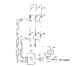
Fig. 1 is a schematic diagram showing a first
embodiment of this invention.
Fig. 2 is a schematic diagram showing a second
embodiment of this invention.
Fig. 3 is a schematic diagram showing a system used an
over-voltage protection circuit.
Fig. ~ is a schematic diagram showing a prior art
example.
Description of the preferred embodiments
The following is a description of an em~odiment of this
invention with reference to the drawings.
Fig. 1 is a schematic diagram of a first embodiment of
this invention, and the same symbols are given to devices
which operate with the same functions as in Figs. 3 and 4.

2 ~ ~
And in this embodiment, VBO free thyristors are used as the
switching element.
In Fig. 1, 50 is a current sensor which detects the
current flowin~ in the VBO free thyristor circuit; 51 is a
level sensor which detects whether or not the output signal
of current sensor 50 has exceeded a pre-set level; 52 is a
NOT circuit which reverses signals; 53 is an AND circuit
which takes a logical product and 54 is an OR circuit which
takes a logical sum.
In the circuit in Fig. 1, if, for instance, VBO free
thyristor 11 i5 assumed to arc due to over-voltage, the
shared voltage of VBO free thyristor 21 will increase due to
the firin0 of VBO free thyristor ll. Thus, VBO free
thyristor 12 will also fire almost simultaneously due to
over-voltage. In this way, one of the three parallel
circuits which includes VBO free thyristors 11 and 12 will
fire. For this reason, a current will flow through VBO free
thyristors ll and 12, and this current will be detected by
current sensor 50. If this current exceeds a pre set level,
the level sensor will detect this and ~enerate an output.
In order to detect that the firin~ is due to an over~
volta~e, the logical product with the reverse signal of the
ON comr~nd is taken, by AND circuit 53. By this means, the
fact that some VBO free thyristors have fired and a current
i5 flowing in a state where there is no ON command, that is
to say that they have fired due to an over-voltage, can be
-- 6 --

~2296
detected.
The logic sum of the output of AND circuit 53 with ~he
ON command is taken by OR circuit 54, and supplied to gate
circuit 55. When a signal is inputted, gate circuit 55
impresses firing pulses on all VBO free thyristors 11, 12,
21, 22, 31 and 32 simultaneously.
In the above way, when VBO free thyristor 11 has fired
due to over-voltage, the fact that a current is flowing is
detected and firing pulses are also applied to the other VBO
free thyristors 21, 22, 31 and 32. Therefore, ~ince VBO
free thyristors 21, 22, 31 and 32 also arc, the VBO free
thyristors of all three parallels fire. Thus, current
concentration in one circuit can be prevented.
Fig. 2 is a schematic diagram showing a second
embodiment of this invention. In Fi~ure 2, 56 are voltage
sensors which detect the voltages between the anodes and
cathodes of VBO free thyristors 11 and 12, 21 and 22, 31 and
32. Also in Fig. 2, instead of detecting the firing of a
VBO free thyristor using current as in Fig. 1, the over-
voltage firing of a VBO free thyristor is detected by the
fact that the voltage between the anode and the cathode of
the VBO free thyristor caused by that voltage has become
zero. Level sensors 51 in Fig. 2 detect that the voltages
betw~en the anodes and the cathodes have become almost zero.
When a voltage has become almost zero in the state where
there is no ON command, gate circuit 55 supplies firing

~722~6
pulses to all VBO free thyristors 11, 12, 21, 22, 31 and 32
In Fig. 2, voltage sensors 5~ are connec~ed one each to
multiple series devices. However, even if voltage sensors
56 are connected to every individual VBO free thyristor, the
effect of this invention will not be altered.
Also, in Fig. 1, current sensor 50 detects the entire
current. However, even if the current is detected by
connecting current sensors 50 to every individual parallel
circuit, the effect of this invention will not be altered.
Although the invention has been described in its
preferred form with a certain degree of particularity, it is
understood that the present disclosure of the preferred form
may be changed in the details of construction and other
combinations and arrangements of parts may be resorted to
without departing from the spirit and the scope of the
invention sa hereinafter claimed.
; When this invention is used as described above, current
concentration in one of the parallel switching circuits can
be prevented and the switching elements can be prevented
from breaking down.
-- 8 --

Representative Drawing
A single figure which represents the drawing illustrating the invention.
Administrative Status

2024-08-01:As part of the Next Generation Patents (NGP) transition, the Canadian Patents Database (CPD) now contains a more detailed Event History, which replicates the Event Log of our new back-office solution.

Please note that "Inactive:" events refers to events no longer in use in our new back-office solution.

For a clearer understanding of the status of the application/patent presented on this page, the site Disclaimer , as well as the definitions for Patent , Event History , Maintenance Fee  and Payment History  should be consulted.

Event History

Description Date
Inactive: IPC from MCD 2006-03-11
Time Limit for Reversal Expired 2003-06-25
Letter Sent 2002-06-25
Letter Sent 1999-12-06
Grant by Issuance 1997-10-28
Inactive: Application prosecuted on TS as of Log entry date 1997-08-22
Inactive: Status info is complete as of Log entry date 1997-08-22
Pre-grant 1997-07-16
Notice of Allowance is Issued 1997-01-28
Application Published (Open to Public Inspection) 1992-12-27
All Requirements for Examination Determined Compliant 1992-06-25
Request for Examination Requirements Determined Compliant 1992-06-25

Abandonment History

There is no abandonment history.

Fee History

Fee Type Anniversary Year Due Date Paid Date
Final fee - standard 1997-07-16
MF (patent, 6th anniv.) - standard 1998-06-25 1998-05-04
MF (patent, 7th anniv.) - standard 1999-06-25 1999-05-03
MF (patent, 8th anniv.) - standard 2000-06-26 1999-05-18
MF (patent, 9th anniv.) - standard 2001-06-25 2001-05-16
Owners on Record

Note: Records showing the ownership history in alphabetical order.

Current Owners on Record
KABUSHIKI KAISHA TOSHIBA
Past Owners on Record
TAKEO KANAI
Past Owners that do not appear in the "Owners on Record" listing will appear in other documentation within the application.
Documents

To view selected files, please enter reCAPTCHA code :


To view images, click a link in the Document Description column. To download the documents, select one or more checkboxes in the first column and then click the "Download Selected in PDF format (Zip Archive)" or the "Download Selected as Single PDF" button.

List of published and non-published patent-specific documents on the CPD .

If you have any difficulty accessing content, you can call the Client Service Centre at 1-866-997-1936 or send them an e-mail at CIPO Client Service Centre.


Document
Description 
Date
(yyyy-mm-dd) 
Number of pages   Size of Image (KB) 
Claims 1993-12-15 2 38
Cover Page 1993-12-15 1 14
Abstract 1993-12-15 1 22
Drawings 1993-12-15 3 56
Description 1993-12-15 8 235
Cover Page 1997-10-27 1 54
Representative drawing 1997-10-27 1 6
Maintenance Fee Notice 2002-07-23 1 177
Correspondence 1999-12-06 1 12
Fees 1997-04-04 1 62
Fees 1996-04-09 1 62
Fees 1995-04-11 1 66
Fees 1994-03-31 1 81
Courtesy - Office Letter 1992-12-01 1 40
PCT Correspondence 1997-07-16 2 45