Language selection

Search

Patent 2072426 Summary

Third-party information liability

Some of the information on this Web page has been provided by external sources. The Government of Canada is not responsible for the accuracy, reliability or currency of the information supplied by external sources. Users wishing to rely upon this information should consult directly with the source of the information. Content provided by external sources is not subject to official languages, privacy and accessibility requirements.

Claims and Abstract availability

Any discrepancies in the text and image of the Claims and Abstract are due to differing posting times. Text of the Claims and Abstract are posted:

  • At the time the application is open to public inspection;
  • At the time of issue of the patent (grant).
(12) Patent: (11) CA 2072426
(54) English Title: SIGNAL GENERATING DEVICE
(54) French Title: DISPOSITIF GENERATEUR DE SIGNAUX
Status: Expired and beyond the Period of Reversal
Bibliographic Data
(51) International Patent Classification (IPC):
  • H03B 01/00 (2006.01)
  • H03B 05/32 (2006.01)
  • H03K 03/03 (2006.01)
(72) Inventors :
  • MUROOKA, FUMIO (Japan)
(73) Owners :
  • CANON KABUSHIKI KAISHA
(71) Applicants :
  • CANON KABUSHIKI KAISHA (Japan)
(74) Agent: SMART & BIGGAR LP
(74) Associate agent:
(45) Issued: 1998-12-08
(22) Filed Date: 1992-06-26
(41) Open to Public Inspection: 1993-01-03
Examination requested: 1992-06-26
Availability of licence: N/A
Dedicated to the Public: N/A
(25) Language of filing: English

Patent Cooperation Treaty (PCT): No

(30) Application Priority Data:
Application No. Country/Territory Date
03-161519 (Japan) 1991-07-02

Abstracts

English Abstract


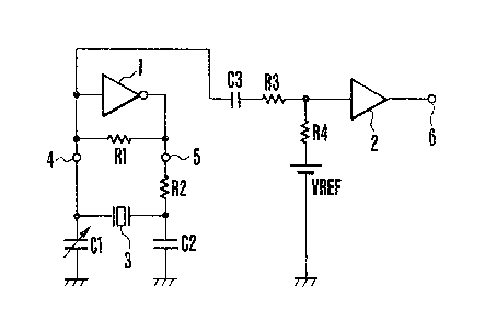
A signal generating device according to the present
invention is a device for generating a signal. The device
includes a crystal oscillating element and an inverter
connected in parallel with the crystal oscillating element.
The device is arranged to adjust the amplitude of a signal
produced at an input side of the inverter and to capacity-couple
the signal produced at the input side of the inverter
to an amplifier circuit so that the signal produced at the
input side of the inverter is amplified. Accordingly, it is
possible to realize a simple construction which includes a
reduced number of terminals, which is suited to high-density
mounting or is suitably formed as an integrated circuit, and
which can be easily reduced in cost.


French Abstract

La présente invention est un dispositif générateur de signaux. Ce dispositif comprend un oscillateur à cristal et un inverseur connecté en parallèle avec cet oscillateur. Il est conçu de façon à ajuster l'amplitude du signal d'entrée de l'inverseur et de transmettre ce signal à un circuit amplificateur par l'intermédiaire d'un couplage capacitif pour l'amplifier. Il peut être construit de façon simple avec des bornes en nombre restreint, ce qui le rend approprié aux montages à grande densité ou aux circuits intégrés et en réduit facilement le prix de revient.

Claims

Note: Claims are shown in the official language in which they were submitted.


THE EMBODIMENTS OF THE INVENTION IN WHICH AN EXCLUSIVE
PROPERTY OR PRIVILEGE IS CLAIMED ARE DEFINED AS FOLLOWS:
1. A signal generating device for generating a
signal, comprising:
(a) a crystal oscillating element;
(b) an inverter connected in parallel with said
crystal oscillating element;
(c) amplitude adjusting means for adjusting an
amplitude of a signal produced at an input side of said
inverter;
(d) capacitive-coupling means for providing
capacitive-coupling of the signal produced at the input
side of said inverter;
(e) a level adjusting circuit for adjusting a
level of the signal fed through said capacitive-coupling
means; and
(f) an amplifier circuit for amplifying the
signal having its level adjusting circuit and for
outputting the amplified signal.
2. A signal generating device according to claim
1, wherein said crystal oscillating element includes a
variable capacitor for adjusting an oscillation
frequency.
3. A signal generating device according to claim
1, wherein said inverter includes an inverter element
having a CMOS or Bi-CMOS construction.
4. A signal generating device according to claim
1, wherein said amplitude adjusting means includes a
capacitor and a resistor.
- 9 -

5. A signal generating device according to claim 1,
wherein said capacity-coupling means includes a coupling
capacitor.
- 10 -

Description

Note: Descriptions are shown in the official language in which they were submitted.


2~7~')6
Background of the Invention:
Field of the Invention:
The present invention relates to a signal
generating device for generating a signal and, more
particularlyr to a signal generating device for generating a
carrier signal for use in down-converting a chrominance
signal.
Description of the Related Art:
A carrier signal generating device is known as one
example of a signal generating device for genera-ting a
signal. The carrier signal generating device is arranged to
generate a carrler signal used in the down-conversion of a
chrominance signal which is performed for recording a
standard color television signal on a video tape in a video
tape recorder~
Fiy. 1 is a block diagram sche.matically showing the
arrangement of a chro~;n~nce signal down~converting circuit
provided with a conventional carr.ier signal generating
device.
As shown in Fig. 1, a chrominance signal
~fl=30S8MHz~ inputted through an input terminal 14 is
frequency-converted in a frequency converter 15 by using a
carrier signal (f2=4.32MHz) generated fro~l the carrier signal
generatiny device 11.
The frequency converter 15 outputs the chrominance
signal whose fr~quency has be~n converted into a frequency
~f2~fl) to a band-pass filter ~BPF) 17 over a signal line 16.
The BP~ 17 extracts a signal of frequency f2-fl-743KHz from
~ .

~72~2~
the input chrominance signal and outputs the extracted signal
through an output t~rm; n~l 18 .
~ he carrier signal (f2=4.32MHz~ is required to be a
signal of single frequency free from high-frequency
components of second order or higher~ Accordingly~ as shown
in Fig. 1, a trap circuit 13 made up of a ceramics filter or
the like is used to el; ;n~te such high-frequency components
from the carrier signal generated from the carrier signal
generating device 11 provided with a crystal oscillator.
After the high-frequency components have been eliminated from
the carrier signal by the trap circuit 13, the carrier signal
is suppli~d to the frequency converter 15.
As described above, in the conventional circuit,
the carrier signal generating device 11 provided with the
crystal oscillator is employed to generate the carrier signal
having a stab1e single frequency~ However, since the carrier
signal outputted from the c~rrier signal generating device 11
contains a distortion due to the characteristics of the
carrier signal generating device 11 itself, the trap circuit
13 needs to be added for ~l;r;nating such a distortion.
However, since the trap circuit 13 is made up of,
for example, a ceramics filter, it is difficult to form the
trap circuit 13 as a small-size element. This disadvantage
hinders implementation of high density mounting and cost
reduction. In addition, if the carrier signal generating
circuit 11 and the frequency converter 15 are to be formed as
an integra-ted circuit, it is necessary to provid~ a terminal
12 for connection with the trap circuit 13 and the total
-- 3 --

2072qL2~
number of te ;~ls mus~ be increased.
Summary of the Invention:
It is, therefore, an object of the present
invention to provide a signal generating device which makes
it possible to solve the above-described problems~
Another object of the present invention is to
provide a signal generating device having a simple
arrangement which includes a reduced number of terminals,
which is suited to high-density mounting or is suitably
formed as an integrated circuit, and which can be easily
reduced in cost.
To achieve the above objects, in accordance with
one aspect of the present invention, there is provided a
signal generating device for genera~ing a signal, which
comprises a crystal oscillating element, an inverter
connected in parallel with the crystal oscillating element,
amplitude adjusting means for adjusting an amplitude of a
signal produced at an input side of the inverter, capacity-
coupling means for providing capacity-coupling of the signal
produced at the input side of the inverter, and an amplifier
circuit for amplifying a signal supplied via the capacity-
coupling means.
The above and other objects, features and
advantages of the present invention will become apparent from
the following detailed descrlption of a preferred embodiment
of the present inventionl taken in conjunction with the
accompanying drawings.
-- 4 --
.
.
:: :

~7~
Brief Description of the Drawings:
Fig. 1 is a block diagram schematically showing the
arrangement of a chlc ;n~nce signal down-conver~ing circuit
provided with a conventional carrier signal generating
device;
Fig. 2 is a diagram showing the circuit arrangement
of a carrier signal genera~ing device to which one embodiment
of the present invention is applied; and
Fig. 3 is a block diagram schematically showing the
circuit arrangement of a chrominance signal down-converting
circuit provided with the carrier signal generating device
shown in Fig. 2.
. ,
Detailed Description of the Preferred Embodiment:
A preferred embodiment of the present invention
will be described below wi~h reference to the accompanying
drawings. ~ '''
Fig~ 2 is a diagram showing the circuit arrangement
of a carrier signal generating device to which one embodiment
of the present invention is applied. Fig. 3 is a block
diagram schematically showing the circuit arrangem~nt of a
chrominanca signal down-converting circuit provided with the
carrier signal generating device shown in Fig. 2.
In Fig. 3, the same reference numerals are used to
denote elements which are substantially identical to the
elements shown in Yig~ 1 t and a detailed description is
omitted.
,
-- 5 --
., . ~ , ~

~7~2~
The circuit arrangement shown in Fig. 2 includes an
inverter 1 having a CMOS or Bi-CMos construction, a feedback
resistor Rl, a crystal oscillator 3, a trimmer capacitor C1
for adjusting an oscillation frequency, a load capacitance
C2l and a resistor R2 for adjusting the amplitude of a si.gnal
produced at the input side of the inverter lo
Normally, a signal waveform appearing at an output
ter~; n~l 5 of the inverter 1 is a rectangular waveform, and
a sine-wave signal of single frequency which is determined by
the resonant frequency of the crystal oscillator 3 is
produced at an input terminal 4 of the inverter 1.
The frequency of the sine-wave signal can be
adjusted chiefly by the tr.immer capacitor C1, and the
amplitude of the sine-wave signal can be freely adjusted by
selecting the value of the resistor R2 and that of the load
capacitance C2 within the range of source voltages of the
inverter 1.
As described above, the sine-wave signal produced
at the input teL ; n~ 1 4 of the inverter 1 is supplied to an
amplifier 2 through a coupling capacitor C3. The sine-wave
signal which has been amplified by the àmplifier 2 is
supplied via an output terminal 6 to the frequency converter
15 shown in Fig. 3 tthe carrier signal generatlng device
shown in Fig. 2 corresponds to a block 10 of Fig. 3).
If it is assumed that the input impedance of the
amplifier ~ is high to a negligible e~tent and that the
respective values of the coupling capacitor C3 and the
resistors R3 and R4 are represented as the relationship
, . .
'' ~ .~ ;'; ~

- 2~7~2~
f2~1/(2~C3(R3+R4)), the amplitude of the sine-wave signal
produced at the input t~ i n~ 1 4 of the inverter 1 is
attenuated to a level represented by R4/(R3+R4). The thus-
obtained signal is supplied to the amplifier 2.
~ he input operating point of the amplifier 2 may be
determined by the voltage level VREF shown in Fig. 2, and the
resistance ratio of the resistor R3 to th~ resistor R4 may be
determined by the range of input voltages of the amplifier 2.
The gain and the output operating point of the amplifier 2
may be determined so that optimum inter~ace conditions can be
realized with respect to the next-stage frequency
converter 15.
If the coupling capacitor C3 is composed of, for
example, a MOS capacitor which is formed as part of an
integrated circuit, a terminal of the capacitor may be
connected so that a parasitic capacitance occurxing between
the coupling capacitor C3 and ground can be produced at the
input terr; n~l 4 of the inverter 1.
AS descrlbed above, according to the present
embodiment, it is possible to generate a carrier signal for
use in frequency-converting a chrominance signal without
eliminating a high-frequency component by means of a trap
circuit in the conventional manner. Accordingly, if a
carrier signal generating device and a frequency converting
circuit are to be formed as an integrated circùit, the number
of terminals or external elements can be reduced so that it
is possible to reduce the size and cost of an integrated-
circuit mounting substrate.
- ~ , -
.
, :., -
- - ~

2~72~2~
As is apparent from the foregoing description,
according to the present embodimen-t, it is possible to
provide a siynal yenerating device which includes a reduced
number of terminals, which is suit0d to high-density mounting
or is suitably formed as an integrated circuit, and which can
ba easily reduced in cost.
-: ~,
;.
:: : : ~,,

Representative Drawing
A single figure which represents the drawing illustrating the invention.
Administrative Status

2024-08-01:As part of the Next Generation Patents (NGP) transition, the Canadian Patents Database (CPD) now contains a more detailed Event History, which replicates the Event Log of our new back-office solution.

Please note that "Inactive:" events refers to events no longer in use in our new back-office solution.

For a clearer understanding of the status of the application/patent presented on this page, the site Disclaimer , as well as the definitions for Patent , Event History , Maintenance Fee  and Payment History  should be consulted.

Event History

Description Date
Time Limit for Reversal Expired 2011-06-27
Letter Sent 2010-06-28
Inactive: IPC from MCD 2006-03-11
Grant by Issuance 1998-12-08
Pre-grant 1998-07-22
Inactive: Final fee received 1998-07-22
Inactive: Received pages at allowance 1998-07-22
Notice of Allowance is Issued 1998-02-10
Letter Sent 1998-02-10
Inactive: Status info is complete as of Log entry date 1998-02-05
Inactive: Application prosecuted on TS as of Log entry date 1998-02-05
Inactive: IPC removed 1997-12-16
Inactive: IPC assigned 1997-12-16
Inactive: Approved for allowance (AFA) 1997-12-16
Inactive: First IPC assigned 1997-12-16
Inactive: IPC assigned 1997-12-16
Application Published (Open to Public Inspection) 1993-01-03
Request for Examination Requirements Determined Compliant 1992-06-26
All Requirements for Examination Determined Compliant 1992-06-26

Abandonment History

There is no abandonment history.

Maintenance Fee

The last payment was received on 1998-05-04

Note : If the full payment has not been received on or before the date indicated, a further fee may be required which may be one of the following

  • the reinstatement fee;
  • the late payment fee; or
  • additional fee to reverse deemed expiry.

Patent fees are adjusted on the 1st of January every year. The amounts above are the current amounts if received by December 31 of the current year.
Please refer to the CIPO Patent Fees web page to see all current fee amounts.

Fee History

Fee Type Anniversary Year Due Date Paid Date
MF (application, 6th anniv.) - standard 06 1998-06-26 1998-05-04
Final fee - standard 1998-07-22
MF (patent, 7th anniv.) - standard 1999-06-28 1999-05-06
MF (patent, 8th anniv.) - standard 2000-06-26 2000-05-04
MF (patent, 9th anniv.) - standard 2001-06-26 2001-06-26
MF (patent, 10th anniv.) - standard 2002-06-26 2002-05-16
MF (patent, 11th anniv.) - standard 2003-06-26 2003-05-20
MF (patent, 12th anniv.) - standard 2004-06-28 2004-05-17
MF (patent, 13th anniv.) - standard 2005-06-27 2005-05-09
MF (patent, 14th anniv.) - standard 2006-06-26 2006-05-05
MF (patent, 15th anniv.) - standard 2007-06-26 2007-05-07
MF (patent, 16th anniv.) - standard 2008-06-26 2008-05-12
MF (patent, 17th anniv.) - standard 2009-06-26 2009-05-14
Owners on Record

Note: Records showing the ownership history in alphabetical order.

Current Owners on Record
CANON KABUSHIKI KAISHA
Past Owners on Record
FUMIO MUROOKA
Past Owners that do not appear in the "Owners on Record" listing will appear in other documentation within the application.
Documents

To view selected files, please enter reCAPTCHA code :


To view images, click a link in the Document Description column. To download the documents, select one or more checkboxes in the first column and then click the "Download Selected in PDF format (Zip Archive)" or the "Download Selected as Single PDF" button.

List of published and non-published patent-specific documents on the CPD .

If you have any difficulty accessing content, you can call the Client Service Centre at 1-866-997-1936 or send them an e-mail at CIPO Client Service Centre.


Document
Description 
Date
(yyyy-mm-dd) 
Number of pages   Size of Image (KB) 
Claims 1998-07-21 2 37
Claims 1997-11-25 2 51
Drawings 1997-11-25 2 18
Abstract 1994-02-25 1 25
Description 1994-02-25 7 247
Drawings 1994-02-25 2 41
Claims 1994-02-25 2 52
Representative drawing 1998-11-30 1 5
Commissioner's Notice - Application Found Allowable 1998-02-09 1 165
Maintenance Fee Notice 2010-08-08 1 170
Fees 1998-05-03 1 37
Fees 2000-05-03 1 31
Correspondence 1998-02-05 1 100
Correspondence 1998-07-21 2 42
Fees 2001-06-25 1 32
Fees 1999-05-05 1 27
Fees 1997-04-29 1 40
Fees 1995-05-18 1 50
Fees 1996-04-30 1 44
Fees 1994-05-03 1 47
Courtesy - Office Letter 1993-03-04 1 43
Prosecution correspondence 1996-04-28 3 47
Prosecution correspondence 1995-12-19 3 99
Prosecution correspondence 1993-10-03 4 131
Examiner Requisition 1995-08-20 2 79
Examiner Requisition 1996-01-29 2 79