Language selection

Search

Patent 2072829 Summary

Third-party information liability

Some of the information on this Web page has been provided by external sources. The Government of Canada is not responsible for the accuracy, reliability or currency of the information supplied by external sources. Users wishing to rely upon this information should consult directly with the source of the information. Content provided by external sources is not subject to official languages, privacy and accessibility requirements.

Claims and Abstract availability

Any discrepancies in the text and image of the Claims and Abstract are due to differing posting times. Text of the Claims and Abstract are posted:

  • At the time the application is open to public inspection;
  • At the time of issue of the patent (grant).
(12) Patent: (11) CA 2072829
(54) English Title: SURFACE PROCESSING JET
(54) French Title: TRAITEMENT D'UNE SURFACE PAR JET
Status: Expired and beyond the Period of Reversal
Bibliographic Data
(51) International Patent Classification (IPC):
  • B08B 3/02 (2006.01)
  • B05B 13/02 (2006.01)
  • B21C 9/00 (2006.01)
  • B21C 43/00 (2006.01)
  • B21C 43/04 (2006.01)
  • C23G 3/02 (2006.01)
  • C25D 17/00 (2006.01)
(72) Inventors :
  • LINDWALL, REINE (Sweden)
(73) Owners :
  • CANDOR SWEDEN AB
(71) Applicants :
  • REINE LINDWALL (Sweden)
(74) Agent: SMART & BIGGAR LP
(74) Associate agent:
(45) Issued: 2003-09-23
(22) Filed Date: 1992-06-30
(41) Open to Public Inspection: 1993-01-02
Examination requested: 1999-06-08
Availability of licence: N/A
Dedicated to the Public: N/A
(25) Language of filing: English

Patent Cooperation Treaty (PCT): No

(30) Application Priority Data:
Application No. Country/Territory Date
91 02031-3 (Sweden) 1991-07-01

Abstracts

English Abstract


A surface processing device for cleaning and other
surface processing of running material, where the material
is passed under movement in a path (19A) through the device,
wherein the device is provided with means, comprising an
inner cavity (13) that is fed with a processing agent under
pressure and has a jet forming slot (20) to direct to the
running material a well defined laminar jet of the process-
ing agent under an acute angle.


Claims

Note: Claims are shown in the official language in which they were submitted.

5
CLAIMS:
1. ~A surface processing device for cleaning and other
surface processing of running material, comprising a body
having a throughbore where the material is passed under
movement in a path (19a) through the device, characterized
in that the body is provided with means, comprising an inner
cavity (13) that is fed with a processing agent under
pressure and has a jet forming slot (20) connecting said
cavity with said throughbore to direct to the running
material a well defined laminar jet of the processing agent
at an acute angle wherein the device includes a bipolar
electric cell having a first electrode (21) forming a wall
portion of said cavity and a second electrode (22) forming a
wall portion of said throughbore downstream from said slot.
2. ~A surface processing device according to claim 1,
characterized in that the acute angle is of the order of
40°-70° degree.
3. ~A surface processing device according to claim l,
characterized in that the jet forming slot (20) is
rotational symmetric and surrounds the path, along which the
material is passed.
4. ~A surface processing device according to claim 1,
characterized in that the jet forming slot has a
height/width ratio of 1:5-10.
5. ~A surface processing device according to claim 1,
characterized in that a plurality of processing units (25,
26, 27), each having an inner cavity (13) and a jet forming
slot (20) are arranged one after the other in the passing
direction of the material.

Description

Note: Descriptions are shown in the official language in which they were submitted.


1
A SURFACE PTtOCEfiBING 1~~YIC3i
The pxesPnt invention relates to a surface processing
device for running material. In the instant case the expres-
sion running material is used to include wires, strips,
tubes, and the like, preferably of metal. The invention has
been created in connection with works with wire-shaped
material of metall., and, therefore, the invention will be
disclosed below with reference thereto, however, while not
being limited to be utilized only in connection with pro-
cessing of metal wires.
When a metal wire shall be processed further by a
mechanical processing or shall be provided with a superfi-
cial cover the surface of the wire has to be free from all
kinds of contaminations, e.g. in the shape of oxydes, grea-
se, drawing agents or the like. Usual. ways of remQVing such
aantaminatians are by means of acids or de~-greasing agents.
In same cases the contaminations are removed machania~ally,
e.g. by brushing. 1n processing by means of acids ox de-
greasing agents the wire is immersed or drawn through a
suitable cleansing bath for a predetermined period ai time.
Often, this procedure is quite time consuming, which makes
it difficult to arrange the equ~.pment in question in line
with other production equipments. To cut down the processing
time at least to some extent it is possible to utilize
electrolytic methods, and another way is to utilize ultra
sound.
~rbe present invention has aimed at providing a surface
processing device, by the utilization of which the running
through time of the wire is reduced considerably, as com-
pared to the running through time with the ~ri.or art de-
vices.
To the just mentioned end the su~'face processing device
according to the present invention is characterized essen-
tially in that the device is provided with means, comprising
an inner cavity that is fed with a processing agent under
pressure and has a jet forming slot to direct to the running
material a well defined laminar jet of the processing agent
under an acute angle, preferably of the order of ~40-?0°.

CA 02072829 2002-10-30
23038-94
2
It is particularly advantageous that the jet
forming slot is rotational symmetric and surrounds the path,
along which the material is passed.
Further, according to the present invention, it is
preferred that an electric electrode is disposed in the said
cavity, whereby preferably a further electrode is disposed,
in the passage direction of the material, slightly spaced
from the jet forming slot, whereby a bipolar electrolyte
cell is formed.
In a practical embodiment it is preferred,
according to the invention, that a plurality of processing
units, each having an inner cavity and a jet forming slot
are arranged one after the other in the passing direction of
the material.
In accordance with the present invention, there is
provided a surface processing device for cleaning and other
surface processing of running material, comprising a body
having a throughbore where the material is passed under
movement in a path through the device, characterized in that
the body is provided with means, comprising an inner cavity
that is fed with a processing agent under pressure and has a
jet forming slot connecting said cavity with said
throughbore to direct to the running material a well defined
laminar jet of the processing agent at an acute angle
wherein the device includes a bipolar electric cell having a
first electrode forming a wall portion of said cavity and a
second electrode forming a wall portion of said throughbore
downstream from said slot.

CA 02072829 2002-10-30
23038-94
2a
The invention will be disclosed in more details below
with reference had to the accompanying drawing.
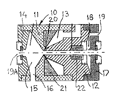
Figure 1 is an axial longitudinal section op a first
embodiment of a surface processing device according to the
present invention, picked as an example)
Figure 2 shows, similarly in an axial longitudinal
section, a second embodiment of a surface processing device
according to the invention, comprising three so called jet
cells, coupled in a series.
The surface processing device according to the inven-
tion as shown in Figure 1 comprises an essentially cylindri-
cal, tube shaped body, generally denoted 10, which has a
transverse wall 11. Into the tube shaped body 10 there is
inserted a plug 12 which, together with the transverse wall,
defines an annular cavity 13. At its left end, as shown in
the drawing, the tubular body ~.p is provided with an end
wall 14 which, together with a recess in the transverse wall
11, forms a drainage chamber 15 that opens outwardly through
an outlet 16.
At the right hand end of the plug 12, as shown in the
drawing, there is provided an end wall 17 which, together
w~,th the end surface of the plug 12, forms a so called air
wiper is that is fed with air from the outside through an
air inlet 19.

207229
3
All of the above mentioned details are passed through
by a central, axial bare 19A through which the wire (not
shown) runs during its passage through the surface process-
ing device aaoording to the present invention.
The annular cavity 13 opens towards the axially
throughgoing bore 19A through an annular slot 20, the gene-
ratrix of which forms an angle with the centre line of the
axially througrigoing bore 19&, viz. an angle of the order of
40-70°.
In the annular cavity 13 there is arranged an electrode
21, and at the right hand end of the plug ~.2, as shown in
the drawing, there is arranged another electrode.22. In the
e:cample both of the electrodes 21, 22 are ring shaped which
is conceived as being most advantageous.
In operation, the wire (not shown) is passed with a
suitable speed through the axially throughgoing bore 19A in
direction from the left towards the right. A suitable clean-
sing agent is fed to the cavity 13 under a suitable pres-
sure, viz. of the order of 5 - 15 kp, and emerges through
the slat 20 in the shape of an annular, wire surrounding
laminar jet of small width, xt~d indeed of such a small width
that the jet acts like a knife. This results in that the
wire surface is processed by the cleansing agent under a
comparatively high pressure, and that the contamining par-
ticles that are freed thereby are quickly passed away from
the wire surface to be passed out through the outlet 16.
The eleotrpdes 2,1 and 22 do not appear to be indis-
pensible for the proper operation of the surface processing
device according to the invention but they enhance the
cleaning effect further. As shown the electrodes 21, 22 are
arranged in such a manner that a bi-polar airquit is formed
within the cell. If the electrode 21, which is disposed
within the cavity 13, is connected to the minus pole of a
rectifier whereas the other electrode 22, which surrounds
the thread, is connected to the plus pole of the rectifier,
then the wire surface will becomes anadic under the narrow
bet of cleansing agent. Thereby, the resistive layer of
solved contaminants and metal cones that surrounds the wire

20'2829
4
will be dissolved and permits a higher current to pass
through the cell, which leads to an accelerated dissolv-
ing/cleaning of the thread surface. By tests current den-
sities of more than 1000 R1/dm2 and up to ten timef~ that
amount have been noted.
=f only an anodic or catodic processing o~ the wire is
desired then a contact shoe (not shown) sliding against the
running wire may transmit the necessary current.
A further application of the above described surface
processing device according to the present invention, be-
sides as a cleansing device, is as a quick plating device,
which is possible because of the high flow speed of the
electrolyte and the high current density that are possible.
A conceived surface processing device according to the
invention, adapted for actual production, is shown in ~i.gurs
2, This device comprises three so palled jet cells 25, 26,
27 of the general type that has been described above with
reference had to the jet cell 10. These jet Cell era ar-
ranged one after the other and in direct contact with each
other in the passage direction of the wire (not shown) and
the two outer cells 25, 27 are provided with end walls 1.4,
17, respectively, in similar way as has been described
above. Thereby, the wire shaped material may be flushed with
water in one. or more of the cells.
A number of modifications and alterations as to details
may be carried out within the scope o~ the invention.

Representative Drawing
A single figure which represents the drawing illustrating the invention.
Administrative Status

2024-08-01:As part of the Next Generation Patents (NGP) transition, the Canadian Patents Database (CPD) now contains a more detailed Event History, which replicates the Event Log of our new back-office solution.

Please note that "Inactive:" events refers to events no longer in use in our new back-office solution.

For a clearer understanding of the status of the application/patent presented on this page, the site Disclaimer , as well as the definitions for Patent , Event History , Maintenance Fee  and Payment History  should be consulted.

Event History

Description Date
Time Limit for Reversal Expired 2008-06-30
Letter Sent 2007-07-03
Inactive: Office letter 2007-01-09
Inactive: Corrective payment - s.78.6 Act 2006-12-11
Inactive: IPC from MCD 2006-03-11
Grant by Issuance 2003-09-23
Inactive: Cover page published 2003-09-22
Pre-grant 2003-06-27
Inactive: Final fee received 2003-06-27
Notice of Allowance is Issued 2003-02-11
Letter Sent 2003-02-11
Notice of Allowance is Issued 2003-02-11
Inactive: Approved for allowance (AFA) 2003-01-27
Amendment Received - Voluntary Amendment 2002-10-30
Inactive: S.30(2) Rules - Examiner requisition 2002-05-01
Inactive: IPC assigned 2001-05-07
Inactive: IPC removed 2001-05-07
Inactive: IPC assigned 2001-05-07
Inactive: IPC removed 2001-05-07
Inactive: IPC assigned 2001-05-07
Inactive: First IPC assigned 2001-05-07
Inactive: IPC assigned 2001-05-07
Inactive: Application prosecuted on TS as of Log entry date 1999-06-21
Letter Sent 1999-06-21
Inactive: Status info is complete as of Log entry date 1999-06-21
Inactive: Entity size changed 1999-06-21
All Requirements for Examination Determined Compliant 1999-06-08
Request for Examination Requirements Determined Compliant 1999-06-08
Application Published (Open to Public Inspection) 1993-01-02

Abandonment History

There is no abandonment history.

Maintenance Fee

The last payment was received on 

Note : If the full payment has not been received on or before the date indicated, a further fee may be required which may be one of the following

  • the reinstatement fee;
  • the late payment fee; or
  • additional fee to reverse deemed expiry.

Please refer to the CIPO Patent Fees web page to see all current fee amounts.

Fee History

Fee Type Anniversary Year Due Date Paid Date
MF (application, 5th anniv.) - standard 05 1997-06-30 1997-06-18
MF (application, 6th anniv.) - standard 06 1998-06-30 1998-06-16
MF (application, 7th anniv.) - standard 07 1999-06-30 1999-06-08
Request for examination - standard 1999-06-08
MF (application, 8th anniv.) - standard 08 2000-06-30 2000-06-01
MF (application, 9th anniv.) - standard 09 2001-07-02 2001-06-01
MF (application, 10th anniv.) - standard 10 2002-07-01 2002-06-04
MF (application, 11th anniv.) - standard 11 2003-06-30 2003-06-02
Final fee - standard 2003-06-27
MF (patent, 12th anniv.) - standard 2004-06-30 2004-05-17
MF (patent, 13th anniv.) - standard 2005-06-30 2005-05-16
MF (patent, 14th anniv.) - standard 2006-06-30 2006-05-15
2006-12-11
MF (application, 2nd anniv.) - small 02 1994-06-30
Owners on Record

Note: Records showing the ownership history in alphabetical order.

Current Owners on Record
CANDOR SWEDEN AB
Past Owners on Record
REINE LINDWALL
Past Owners that do not appear in the "Owners on Record" listing will appear in other documentation within the application.
Documents

To view selected files, please enter reCAPTCHA code :


To view images, click a link in the Document Description column. To download the documents, select one or more checkboxes in the first column and then click the "Download Selected in PDF format (Zip Archive)" or the "Download Selected as Single PDF" button.

List of published and non-published patent-specific documents on the CPD .

If you have any difficulty accessing content, you can call the Client Service Centre at 1-866-997-1936 or send them an e-mail at CIPO Client Service Centre.


Document
Description 
Date
(yyyy-mm-dd) 
Number of pages   Size of Image (KB) 
Representative drawing 1998-09-04 1 14
Claims 2002-10-30 1 39
Description 2002-10-30 5 196
Representative drawing 2003-08-21 1 21
Cover Page 2003-08-21 1 46
Drawings 1993-11-06 1 45
Claims 1993-11-06 1 38
Description 1993-11-06 4 165
Abstract 1993-11-06 1 11
Cover Page 1993-11-06 1 11
Reminder - Request for Examination 1999-03-02 1 117
Acknowledgement of Request for Examination 1999-06-21 1 179
Commissioner's Notice - Application Found Allowable 2003-02-11 1 160
Maintenance Fee Notice 2007-08-14 1 172
Correspondence 1995-09-12 6 166
Correspondence 2003-06-27 1 33
Fees 1995-09-07 1 22
Fees 1998-06-16 1 46
Fees 2000-06-01 1 40
Correspondence 2007-01-09 1 15
Fees 1996-06-25 1 37
Fees 1995-07-27 1 34
Fees 1994-06-20 1 31