Language selection

Search

Patent 2074127 Summary

Third-party information liability

Some of the information on this Web page has been provided by external sources. The Government of Canada is not responsible for the accuracy, reliability or currency of the information supplied by external sources. Users wishing to rely upon this information should consult directly with the source of the information. Content provided by external sources is not subject to official languages, privacy and accessibility requirements.

Claims and Abstract availability

Any discrepancies in the text and image of the Claims and Abstract are due to differing posting times. Text of the Claims and Abstract are posted:

  • At the time the application is open to public inspection;
  • At the time of issue of the patent (grant).
(12) Patent: (11) CA 2074127
(54) English Title: OPTICAL IMAGING SYSTEM WITH A PLURALITY OF IMAGE PLANES
(54) French Title: SYSTEME D'IMAGERIE OPTIQUE AYANT UNE PLURALITE DE PLANS D'IMAGE
Status: Expired and beyond the Period of Reversal
Bibliographic Data
(51) International Patent Classification (IPC):
  • G01C 11/02 (2006.01)
(72) Inventors :
  • DIEHL, HERMANN (Germany)
  • MULLER, FRANZ (Germany)
(73) Owners :
  • LFK-LENKFLUGKORPERSYSTEME GMBH
(71) Applicants :
  • LFK-LENKFLUGKORPERSYSTEME GMBH (Germany)
(74) Agent: MARKS & CLERK
(74) Associate agent:
(45) Issued: 1998-01-06
(22) Filed Date: 1992-07-17
(41) Open to Public Inspection: 1993-01-19
Examination requested: 1992-11-24
Availability of licence: N/A
Dedicated to the Public: N/A
(25) Language of filing: English

Patent Cooperation Treaty (PCT): No

(30) Application Priority Data:
Application No. Country/Territory Date
P 41 23 791.9-31 (Germany) 1991-07-18

Abstracts

English Abstract


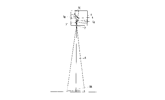
In this optical imaging system the same object section is
imaged by optical means on three spatially separate image planes.
Surface sensors A, B, C of identical width which in turn comprise
optoelectronic sensor elements arranged in the manner of a matrix
are arranged in the three image planes at a distance from one
another in parallel rows and are offset relative to one another
from one row to the other. The three grids of surface sensors
which are accordingly formed are offset relative to one another
from one image plane to the other in such a way that the object
section is detected without gaps by means of the surface sensors
A, B and C during optical superposition. Thus, large surface
area pictures with high resolution can be taken with the use of
conventional surface sensors, e.g. of the CCD type. Due to the
special arrangement of the surface sensors, three image planes
with the corresponding optical means, e.g. three lenses or less
than three lenses and additional beam splitter systems such as
semipermeable mirrors or prisms, are sufficient.


French Abstract

Dans un système imageur optique, la même partie d'objet est imagée par des moyens optiques sur trois plans image spatialement distincts. Des capteurs de surface A, B et C de largeur identique, comprenant eux-mêmes des éléments optoélectroniques sensibles disposés en forme de matrice, sont placés dans les trois plans image à une certaine distance les uns des autres, en rangées parallèles, et sont décalés les uns par rapport aux autres d'une rangée à l'autre. Les trois grilles de capteurs de surface ainsi formées sont décalées les unes par rapport aux autres d'un plan image à l'autre de façon que la partie d'objet soit détectée sans discontinuité au moyen des capteurs de surface A, B et C pendant la superposition optique. Ainsi, de grandes images haute résolution peuvent être prises à l'aide de capteurs de surface classique, p. ex. de type DTC. Étant donné le montage particulier des capteurs de surface, trois plans image avec les moyens optiques correspondants, p. ex. trois lentilles ou moins et des systèmes de séparation de faisceau supplémentaires tels que prismes ou miroirs semi-perméables, sont suffisants.

Claims

Note: Claims are shown in the official language in which they were submitted.


THE EMBODIMENTS OF THE INVENTION IN WHICH AN EXCLUSIVE
PROPERTY OR PRIVILEGE IS CLAIMED ARE DEFINED AS FOLLOWS:
1. Optical imaging system having a plurality of
separate image planes (E A, E B, E C) in which there is a
plurality of rectangular or square surface sensors (A, B, C)
which are arranged at a distance from one another and in
turn comprise a number of optoelectronic sensor elements (S)
arranged in rows and columns, and having optical means (2,
3, 4) which are adjusted or adjustable in such a way that
they image a same object section (OA) on each of the image
planes (E A, E B, E C), characterized in that
- there are only three separate image planes (E A, E B, E C),
- surface sensors (A, B, C) of the same width (d A, d B, d c)
are arranged at a distance from one another in adjacent
parallel rows (R1 etc.),
- distances (.DELTA.A, .DELTA.B, .DELTA.C) between adjacent surface sensors
within a row are greater than their width and are
simultaneously given by a sum of the widths (d A, d B, d c)
of one of surface sensors located in each of the two other
image planes,
- the surface sensors are offset relative to one another in
two immediately adjacent rows by an amount greater than
their own width,
- and grids of surface sensors formed in this way are offset

-11-
relative to one another from one image plane to the other in
such a way that the imaged object section (OA) is detected
without gaps by the totality of surface sensors in optical
superposition of the image planes.
2. Imaging system according to claim 1, characterized in that
the surface sensors (A, B, C) of all three image planes (E A, E B,
E C) have the same width.
3. Imaging system according to claim 2, characterized in that
the surface sensors (A, B, C) are offset relative to one another
in two immediately adjacent rows by 1.5 times their width.

Description

Note: Descriptions are shown in the official language in which they were submitted.


207~1~7
OPTICAL IMAGING SYSTEM WITH A PLURALI~Y OF IMAGE PLANES
The invention is directed to an optical imaging system
having a plurality of separate image planes in which, in each
instance, there is a plurality of rectangular or square surface
sensors which are arranged at a distance from one another and in
turn comprise a number of optoelectronic sensor elements arranged
in rows and columns, and having optical means which are adjusted or
adjustable in such a way that they image the same object portion
on every image plane.
Such an imaging system is known from DE-A1 34 28 325 which
describes an imaging system which is also usable for
photogrammetric purposes and in which four optically parallel
beam paths can be represented by means of four individual lenses.
The four individual lenses are adjusted in such a way that the
same object section is imaged in the four resulting image planes.
In each of the four separate image planes, four square surface
sensors are arranged at distances relative to one another which
are smaller than their own width. These surface sensors can be
CCD sensor blocks formed in the manner of a matrix from
optoelectronic sensor elements. The quadruplicate groups of
these surface sensors are offset relative to one another from one
image plane to the other in such a way that the imaged obj ect
section is covered without gaps by the totality of surface
sensors when the four image planes are optically superimposed.
The cost in apparatus incurred by the use of four lenses is thus

CA 02074127 1997-03-11
relatively high in this known imaging system. Moreover, due
to the relatively small distances between the surface
sensors, there is considerable overlapping in certain
boundary or edge areas of the surface sensors so that image
points situated in these areas are detected two or even
three times in all by sensor elements of different image
planes. Thus, there are considerably more sensor elements
than would be needed for detecting the object section
without gaps and without redundancy together with a
correspondingly greater amount of image information to
process.
According to the invention, the following
characteristic features are provided: there are only three
separate image planes; surface sensors of identical width
are arranged at a distance from one another in adjacent
parallel rows in every image plane; the distances between
the surface sensors within one row are greater than their
width and are, at the same time, given by the sum of the
widths of one of the surface sensors located in each of the
two other image planes; the surface sensors in two
immediately adjacent rows are offset relative to one another
by

_3_ 207~7
more than their own width; the grids of surface sensors formed in
this way are offset relative to one another from one image plane
to the other in such a way that the imaged object section is
detected without gaps by the totality of surface sensors when the
image planes are optically superimposed.
Accordingly, the imaging system of the invention makes do
with only three separate image planes. The respective optical
means can be formed by three separate lenses or by less than
three lenses and, additionally, by semipermeable mirrors or
prisms. The lenses, and also the mirrors, if used, must be
adjusted in,such a way that the same object section is imaged in
every image plane. The surface sensors arranged in parallel rows
in the individual image planes are at distances from one another
within the rows which are greater than their respective widths.
At the same time, the surface sensors arranged in two immediately
adjacent rows are offset relative to one another by more than
their own width and thus do not contact one another and are
arranged "on gaps" so to speak. This takes into account the fact
that the surface sensors, which comprise e.g. 1000 x 1000 sensor
elements arranged in lines and gaps in the manner of a matrix and
have an outer border which is not provided with such elements,
can not be placed adjacent to one another without gaps with
respect to the optically sensitive surfaces in practical
execution. Therefore, the statements made here respecting width

207~ 27
--4--
and distances of the surface sensors refer to their optically
sensitive surfaces containing sensor elements. Due to the mutual
offsetting of the surface sensors in immediately adjacent rows, a
grid of surface sensors arranged at regular intervals occurs in
every image plane. The distances between the surface sensors
within a row, apart from the fact that they are to be greater
than their own width, are dimensioned in such a way that they
correspond exactly to the sum of the widths of one of the surface
sensors situated in each of the remaining two image planes. The
grids of surface sensors produced in this way are offset relative
to one another in the three image planes in such a way that the
entire image surface is covered by surface sensors without gaps
or overlapping when optically superimposed. The contents of the
image are accordingly detected in their entirety with the lowest
possible expenditure on sensor elements.
In practice, it is preferable that the surface sensors in
all three image planes have the same width. In this case, it is
advisable that the surface sensors located in two immediately
adjacent rows be offset relative to one another by 1.5 times
their width. However, it is not absolutely necessary that all
surface sensors have the same width; rather, surface sensors of
different widths can be used from one image plane to the other.

-5_ 20 7~1 2
Embodiment examples of the invention are explained in more
detail in the following with reference to drawings:
Fig. 1 shows an optical imaging system according to the invention
in the form of a digital camera with a lens and two semipermeable
mlrrors;
Figs. 2a to 2c show an arrangement of surface sensors of the same
width in three separate image planes;
Fig. 2d shows the optical superposition of the grids of surface
sensors according to Figs. 2a to 2c; and
Fig. 3 shows the optical superposition of three grids of surface
sensors of different widths.
A conventional aerial camera, for example, has a picture
ratio or image format of approximately 23 x 23 cm2 with a -
resolution of e.g. 100 line pairs/mm, depending on the film which
is used. A digital camera having the same resolution would then
have to use e.g. a CCD surface sensor with 23,000 x 23,000 sensor
elements arranged in a matrix. Such surface sensors are not
available for the foreseeable future.

207~27
A digital camera 1 according to Fig. 1 can be carried e.g.
by aircraft or satellites for taking pictures of the surface of
the overflown terrain. Of course, it can also be used for other
recording purposes. It comprises a lens 2 and two semipermeable
mirrors 3 and 4 arranged one after the other in the path of the
beam. These mirrors 3 and 4 are advisably inclined at an angle
of 45~ relative to the optical axis 5. The semipermeable mirror
3 can be constructed e.g. in such a way that it lets through two
thirds of the incident intensity and reflects one third, guiding
it to the image plane EA associated with it. The second
semipermeable mirror 4 can then advisably be constructed in such
a way that it lets through one half of the incident intensity and
reflects the other half. Two additional separate image planes EB
and Ec are associated with this second semipermeable mirror 4.
The three image planes are covered by grid-like arrangements of
surface sensors approximately corresponding to Figures 2a to 2c.
These grids are offset relative to one another from one image
plane to the other in such a way that the object section OA being
imaged, e.g. a rectangular or square section of a planar terrain
surface, is detected by the surface sensors of the three image
planes without gaps as a whole, as will be made clear in the
following.
A possibility for the arrangement of surface sensors in
three separate image planes which is preferred for its simplicity

2074127
is indicated in Figs. 2a to 2c. According to Fig. 2a, surface
sensors A of identical width dA are arranged at equal distances
~A in a first image plane EA in immediately adjacent, parallel
rows R1 to R6. The distances ~A of the surface sensors A equal
twice their width dA. This corresponds exactly to the sum of the
widths dB and dC of the individual surface sensors B and C which
are arranged in two additional separate image planes EB and EC
according to Figures 2b and 2c. The surface sensors A are offset
relative to one another in two directly adjacent rows, e.g. R1
and R2, by exactly 1.5 times their width dA. Accordingly they
are arranged "on gaps" and their corners have a sufficient
distance from one another so that there is also no mutual
interference of the optically insensitive edges of the individual
surface sensors A which enclose the shown surfaces and are not
shown in the drawing.
In Fig. 2a, it is indicated in the surface sensor at the
upper right-hand corner that this surface sensor, as well~as all
the others (A, B, C, b, c; D, E, F, e, f), in turn also comprises
optoelectronic sensor elements S, e.g. of the CCD type, which are
arranged in the manner of a matrix, i.e. in lines and gaps.
In Figures 2b and 2c there are also surface sensors b and c
in an edge region of the image planes EB and Ec shown in the
drawing. These surface sensors b and c serve only to complement

2074~ 27
--8--
the entire usable image surface to form a complete rectangle when
the three image planes are optically superimposed according to
Fig. 2d.
Fig. 2d shows the optical superposition of the three image
planes EA to Ec shown in Figures 2a to 2c. The three grids of
surface sensors A, B, C merge with one another without gaps or
overlapping in such a way that the image of the object section OA
is divided without gaps into image elements which are alternately
associated with surface sensors A, B, C and b and c of the three
different separate image planes. To achieve such a covering
without gaps it is necessary to provide for a correspondingly
exact positioning of the surface sensors in the individual image
planes at the inner walls of the camera 1 and for an exact
adjustment of the semipermeable mirrors.
Figure 3 illustrates an example showing that the surface
sensors to be arranged in the three separate image planes~need
not have the same width. The optical superposition of three
image planes is shown. Surface sensors D are arranged in the
first of these image planes, surface sensors E and e are arranged
in the second image plane, and finally surface sensors F and f
are arranged in the third image plane, specifically according to
the distribution given in Fig. 3. The surface sensors D, E and F
have the same widths and also meet the rest of the requirements

2074127
g
to be realized in the invention with respect to the widths and
distances.
In its entirety, the invention provides the possibility of
taking digital, large surface area pictures with high resolution
at a cost in optoelectronic sensor elements and optical auxiliary
means which is reduced to the greatest possible extent. The
sensor elements are preferably CCD sensors which can be read out
in a conventional manner.
The process described in the preceding as optical
superposition primarily refers to the purely fictitious, i.e.
imaginary, superposition of the three image planes, wherein the
deflection of the beam paths by the semipermeable mirrors 3 and 4
can be negated conceptually and the image planes EA and EB
accordingly "fall" on the image plane Ec, together with the grids
of surface sensors A, B and C associated with them. In practice
the total image is first assembled from the image point
information of the surface sensors associated with the three
separate image planes by electronic means in the course of the
digital image evaluation.

Representative Drawing
A single figure which represents the drawing illustrating the invention.
Administrative Status

2024-08-01:As part of the Next Generation Patents (NGP) transition, the Canadian Patents Database (CPD) now contains a more detailed Event History, which replicates the Event Log of our new back-office solution.

Please note that "Inactive:" events refers to events no longer in use in our new back-office solution.

For a clearer understanding of the status of the application/patent presented on this page, the site Disclaimer , as well as the definitions for Patent , Event History , Maintenance Fee  and Payment History  should be consulted.

Event History

Description Date
Inactive: IPC expired 2023-01-01
Inactive: IPC from PCS 2022-09-10
Inactive: First IPC from PCS 2022-09-10
Inactive: IPC expired 2011-01-01
Inactive: IPC from MCD 2006-03-11
Time Limit for Reversal Expired 2003-07-17
Letter Sent 2002-07-17
Inactive: Single transfer 1998-12-04
Grant by Issuance 1998-01-06
Inactive: Status info is complete as of Log entry date 1997-11-03
Inactive: Application prosecuted on TS as of Log entry date 1997-11-03
Pre-grant 1997-09-10
Notice of Allowance is Issued 1997-03-11
Application Published (Open to Public Inspection) 1993-01-19
Request for Examination Requirements Determined Compliant 1992-11-24
All Requirements for Examination Determined Compliant 1992-11-24

Abandonment History

There is no abandonment history.

Maintenance Fee

The last payment was received on 1997-07-10

Note : If the full payment has not been received on or before the date indicated, a further fee may be required which may be one of the following

  • the reinstatement fee;
  • the late payment fee; or
  • additional fee to reverse deemed expiry.

Patent fees are adjusted on the 1st of January every year. The amounts above are the current amounts if received by December 31 of the current year.
Please refer to the CIPO Patent Fees web page to see all current fee amounts.

Fee History

Fee Type Anniversary Year Due Date Paid Date
MF (application, 5th anniv.) - standard 05 1997-07-17 1997-07-10
Final fee - standard 1997-09-10
MF (patent, 6th anniv.) - standard 1998-07-17 1998-06-19
Registration of a document 1998-12-04
MF (patent, 7th anniv.) - standard 1999-07-19 1999-06-16
MF (patent, 8th anniv.) - standard 2000-07-17 2000-06-14
MF (patent, 9th anniv.) - standard 2001-07-17 2001-06-18
Owners on Record

Note: Records showing the ownership history in alphabetical order.

Current Owners on Record
LFK-LENKFLUGKORPERSYSTEME GMBH
Past Owners on Record
FRANZ MULLER
HERMANN DIEHL
Past Owners that do not appear in the "Owners on Record" listing will appear in other documentation within the application.
Documents

To view selected files, please enter reCAPTCHA code :


To view images, click a link in the Document Description column (Temporarily unavailable). To download the documents, select one or more checkboxes in the first column and then click the "Download Selected in PDF format (Zip Archive)" or the "Download Selected as Single PDF" button.

List of published and non-published patent-specific documents on the CPD .

If you have any difficulty accessing content, you can call the Client Service Centre at 1-866-997-1936 or send them an e-mail at CIPO Client Service Centre.

({010=All Documents, 020=As Filed, 030=As Open to Public Inspection, 040=At Issuance, 050=Examination, 060=Incoming Correspondence, 070=Miscellaneous, 080=Outgoing Correspondence, 090=Payment})


Document
Description 
Date
(yyyy-mm-dd) 
Number of pages   Size of Image (KB) 
Abstract 1994-02-25 1 25
Claims 1994-02-25 2 42
Description 1994-02-25 9 268
Drawings 1994-02-25 2 31
Description 1997-03-10 9 314
Abstract 1997-03-10 1 28
Claims 1997-03-10 2 48
Description 1998-08-19 9 314
Representative drawing 1998-01-19 1 3
Courtesy - Certificate of registration (related document(s)) 1999-02-02 1 114
Maintenance Fee Notice 2002-08-13 1 177
Fees 1999-06-15 1 24
Fees 1996-06-23 1 59
Fees 1995-06-22 1 57
Fees 1994-06-22 1 45
Courtesy - Office Letter 1993-01-12 1 40
PCT Correspondence 1997-09-09 1 33
Prosecution correspondence 1997-07-08 1 25
Prosecution correspondence 1993-10-21 8 257
Prosecution correspondence 1992-11-23 2 40