Language selection

Search

Patent 2074628 Summary

Third-party information liability

Some of the information on this Web page has been provided by external sources. The Government of Canada is not responsible for the accuracy, reliability or currency of the information supplied by external sources. Users wishing to rely upon this information should consult directly with the source of the information. Content provided by external sources is not subject to official languages, privacy and accessibility requirements.

Claims and Abstract availability

Any discrepancies in the text and image of the Claims and Abstract are due to differing posting times. Text of the Claims and Abstract are posted:

  • At the time the application is open to public inspection;
  • At the time of issue of the patent (grant).
(12) Patent: (11) CA 2074628
(54) English Title: MULTIPROCESSOR SYSTEM FOR CONDUCTING INITIAL PROCESSING FOR SHARED CIRCUIT
(54) French Title: SYSTEME MULTIPROCESSEUR DE TRAITEMENT INITIAL POUR CIRCUIT MIS EN COMMUN
Status: Deemed expired
Bibliographic Data
(51) International Patent Classification (IPC):
  • G06F 13/376 (2006.01)
  • G06F 9/445 (2006.01)
  • G06F 15/16 (2006.01)
(72) Inventors :
  • KONDOU, SEIJI (Japan)
(73) Owners :
  • NEC CORPORATION (Japan)
(71) Applicants :
(74) Agent: G. RONALD BELL & ASSOCIATES
(74) Associate agent:
(45) Issued: 1999-03-02
(22) Filed Date: 1992-07-24
(41) Open to Public Inspection: 1993-01-27
Examination requested: 1992-07-24
Availability of licence: N/A
(25) Language of filing: English

Patent Cooperation Treaty (PCT): No

(30) Application Priority Data:
Application No. Country/Territory Date
91-187915 Japan 1991-07-26

Abstracts

English Abstract


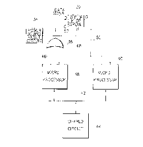
A multi-processor circuit having a plurality of microprocessors coupled to a
shared circuit includes an OR Gate for receiving read signals from each of the
microprocessors, and a D-type flip flop which toggles an initial processing permission signal
between a permission state and an inhibit state. When power is initially supplied to the
circuit, or upon receipt of a reset signal, the initial processing permission signal is set by the
D-type flip flop to the permission state. In this condition, the first microprocessor to recognise
the permission state of the initial processing permission signal issues a "read" signal and
performs an initial processing operation. In response to the "read" signal, the OR gate
transmits a trigger signal to the D-type flip flop to toggle the initial processing permission
signal to the inhibit state, thereby preventing the other microprocessors from performing the
initial processing operation. When all of the microprocessors are operating normally, the
initial processing operation is ordinarily carried out for the shared circuit by the first
microprocessor to generate a read signal. When a failure occurs in one of the
microprocessors, the initial processing can is accomplished by another microprocessor to
start the operation of the multi-processor system. Consequently, an initial processing
operation for the shared circuit can be reliably performed even if one of the microprocessors
is operating abnormally.


French Abstract

Circuit multiprocesseur regroupant un certain nombre de multiprocesseurs couplés à un circuit partagé. Comprend une porte OU pour recevoir des signaux de lecture provenant de chacun des microprocesseurs, et une bascule de type D qui fait alterner un signal de validation de traitement initial entre un état de validation et un état d'invalidation. Lors de la mise sous tension initiale du circuit, ou sur réception d'un signal de remise à zéro, le signal de validation de traitement initial est mis à l'état de validation par la bascule de type D. Ainsi, le premier microprocesseur à reconnaître l'état de validation du signal de validation de traitement initial émet un signal de lecture et exécute un traitement initial. En réponse au signal de lecture, la porte OU transmet un signal de déclenchement à la bascule de type D, visant à faire passer le signal de validation de traitement initial à l'état d'invalidation, ce qui empêche les autres microprocesseurs d'effectuer le traitement initial. Lorsque tous les microprocesseurs fonctionnent normalement, le traitement initial est ordinairement exécuté pour le circuit partagé par le premier microprocesseur afin de produire un signal de lecture. Lorsqu'une défaillance se produit dans un des microprocesseurs, le traitement initial peut être effectué par un autre microprocesseur afin de mettre en marche le système multiprocesseur. Par conséquent, un traitement initial pour le circuit partagé peut être exécuté avec fiabilité même si un des microprocesseurs fonctionne anormalement.

Claims

Note: Claims are shown in the official language in which they were submitted.


THE EMBODIMENTS OF THE INVENTION IN WHICH AN EXCLUSIVE PROPERTY OR
PRIVILEGE IS CLAIMED ARE DEFINED AS FOLLOWS:

1. A multiprocessor system having a plurality of microprocessors connected
to a shared circuit via a shared control line, said multiprocessor system comprising:
resetting means for producing a reset signal;
trigger means for generating a trigger signal in response to a read signal
produced by any of said plurality of microprocessors; and
circuit means for producing an initial processing permission signal in response
to said reset signal and said trigger signal, said initial processing permission signal being
placed in a permission state in response to receipt of said reset signal, and the initial
processing permission signal being switched from said permission state to an inhibition state
in response to receipt of said trigger signal;
wherein each of said microprocessors is capable of monitoring said initial
processing permission signal and producing said read signal substantially simultaneously with
the monitoring;
whereby, one of said plurality of microprocessors performs an initial processingoperation on said shared circuit when said one microprocessor monitors the processing
permission signal in the permission state, and the remaining ones of said plurality of
microprocessors are subsequently inhibited from performing an initial processing operation
on said shared circuit when said microprocessors monitor the processing permission signal
in the inhibition state.


2. A system as claimed in claim 1, wherein said trigger means is a logical OR
circuit, said trigger signal corresponding to a logical sum of read signals produced by said
plurality of microprocessors.

3. A system as claimed in claim 1 or 2, wherein said circuit means for
producing an initial processing permission signal is a D flip flop circuit, an externally
generated data signal being received by a D input of said slip flop, said reset signal being
received by a reset input of said flip flop, said trigger signal being received by a clock input
of said flip flop, and said initial processing permission signal being produced from an output
of said flip flop.


4. A system as claimed in claim 1 or 2, wherein said resetting means is
activated when the multiprocessor system is initially powered.

Description

Note: Descriptions are shown in the official language in which they were submitted.


_ CA 02074628 1998-03-04
-


The present invention relates to a multiprocessor system including a plurality of
microprocessors, and in particular, to a multiprocessor system including a plurality of
microprocessors in which a microprocessor selected therefrom achieves an initial processing
for a circuit to be shared thereamong.
A multiprocessor system is in general constituted with a pluraiity of
microprocessors in which the initial processing is conducted by the microprocessors in a
distributed fashion.
In a case where an initial processing operation, such as a memory check, is
performed on a circuit which is shared among two or more microprocessors, it is necessary
to select a microprocessor therefrom such that the selected microprocessor carries out the
initial processing operation for the shared circuit via a shared control line. The reason for this
is that if the microprocessors simultaneously conduct the initial processing for the shared
circuit, signals from the respective microprocessors collide with each other on the shared
control line, which leads the multiprocessor system to an inoperable state.
To overcome this difficulty, in a conventional multiprocessor system, only one of
the microprocessors is connected to a grounding (GND) potential, (for example, by a
switching circuit) such that the selected microprocessor is connected to the GND potential
while the other microprocessors are not connected to the GND potential. The microprocessor
connected to the GND potential is thereby enabled to accomplish the initial processing
20 operation for the shared circuit.
However, in the conventional multiprocessor system, the GND potential is
monitored by a microprocessor according to the operation of the switching circuit, so as to
select the microprocessor which accomplishes the initial processing operation for the shared
circuit. In consequence, if the microprocessor selected to achieve the initial processing
25 operation cannot conduct the operation due to an abnormal state occurring therein, the
multiprocessor system has no chance to be set to the operable state even when other
microprocessors are operating normally.
It is therefore an object of the present invention to provide a multiprocessor
system in which even when a failure takes place in a microprocessor, the initial processing
30 operation can be accomplished by another microprocessor, thereby removing the above-
stated problem of the conventional multiprocessor system.
In accordance with the present invention, there is provided a multiprocessor
system having a plurality of microprocessors and a shared circuit connected via a shared
control line to the plurality of microprocessors, comprising resetting means for producing a

CA 02074628 1998-03-04
-


reset signal, OR gate means for generating a logical sum between read signals sent from the
microprocessors, and means for receiving a reset signal from the resetting means and being
reset by the reset signal, receiving an output signal produced by the OR gate means and a
data signal fed from a device external with respect to the multiprocessor system, determining
5 a microprocessor among the plurality of microprocessors to conduct an initial processing for
the shared circuit, and producing an initial processing permission signal to inhibit the
microprocessors other than the determined microprocessor from achieving the initial
processing, wherein each the microprocessor outputs, on receiving the initial processing
permission signal, a read signal to the OR gate means so as to carry out the initial
10 processing for the shared circuit when the signal is in a permission state and not to conduct
the initial processing for the shared circuit when the signal is in an inhibit state.
The objects and features of the present invention will become more apparent
from the following detailed description taken in conjunction with the accompanying drawings,
in which:
Figure 1 is a schematic diagram showing the configuration of a conventional
multiprocessor system;
Figure 2 is a block diagram schematically showing the constitution of an
embodiment of a multiprocessor system in accordance with the present invention; and
Figure 3 is a signal timing chart showing operation timings of signals generatedafter the Figure 2 system is powered.
Referring to Figure 1, a conventional multiprocessor system will be described for
a better understanding of this invention. The system of Figure 1 includes a switching circuit
14, microprocessors 16, 18 and 20, and a shared circuit 24. In the switching circuit 14, a
terminal is connected to a grounding potential and another terminal is connected, for
example, to a microprocessor 16 as shown in Figure 1, thereby allowing the microprocessor
16 to monitor a GND signal while preventing the microprocessors 18 and 20 from monitoring
the GND signal. As a result, only the microprocessor 16 monitoring the GND signal
accomplishes the initial processing operation (such as a memory check) for the shared circuit
24, via the shared control line 22.
In this system, however, since the GND signal is monitored, according to the
operation of the switching circuit 14, to select the microprocessor which conducts the initial
processing operation, when a failure occurs, for example, in the microprocessor monitoring
the GND signal (such that the initial processing operation cannot be processed by this

, . CA 02074628 1998-03-04


microprocessor), the system cannot be started at all, even when the other microprocessors
are operating normally.
Referring now to Figures 2 and 3, description will be given of an embodiment of
the present invention. Figure 2 schematically shows an embodiment of the multiprocessor
5 system according to the present invention. This system includes a D flip flop circuit 32, a
power source reset circuit 34, an OR gate 36, microprocessors 38 and 40, and a shared
circuit 44.
The microprocessors 38 and 40 are connected via a shared control line 42 to the
shared circuit 44. Each of these microprocessors 38 and 40 monitors an initial processing
permission signal 50 created from the d flip flop circuit 32. When the signal 50 is at a low
level, the microprocessor having monitored the signal 50 performs the initial processing
operation for the shared circuit 44 via the shared control line 42. In addition, while monitoring
the signal 50, the microprocessor 38 or 40 outputs a read signal 46 or 48, respectively. As
shown in Figure 3, the read signals 46 and 48 are at a high level. After a predetermined
15 period time is elapsed in this state, these signals return to a low level.
On receiving the read signal 46 or 48 respectively from the microprocessor 38
or 40, the OR gate 36 outputs a trigger signal 52 to the D flip flop circuit 32.The D flip flop circuit 32 receives, at a data terminal D thereof, a high-level data
signal from a device external to the multiprocessor system. When this circuit 32 receives the
20 trigger signal 52, at a clock terminal C thereof, the initial processing permission signal 50
from the D flip flop circuit 32 is changed from the low level to the high level. However, when
a reset signal is supplied to the D flip flop circuit 32 from the power source reset circuit 34,
the initial processing permission signal 50 is kept at a low level.
The power source reset circuit 34 keeps its output at a low-level for several
25 milliseconds after power is initially supplied to the multiprocessor system. The circuit 34 then
outputs a high-level signal to reset the D flip flop circuit 32 and thereafter outputs a low-level
signal to release the reset operation, which sets the initial processing permission signal 50
from the D flip flop circuit 32 to the low level.
Next, the operation of the multiprocessor system of Figure 2 will be described in
30 more detail by referring to the signal timing chart of Figure 3.
When the system is powered at a time 54, the D flip flop circuit 32 is reset andhence the initial processing permission signal 50 is at a low level.

CA 02074628 1998-03-04


Subsequently, the microprocessor 38 (Figure 2) monitors the signal 50 and
determines that the signal 50 is at the low level. Consequently the microprocessor 38
performs the initial processing operation for the shared circuit 44 via the shared control line
42. Moreover, while monitoring the signal 50, the microprocessor 38 simultaneously outputs
the read signal 46. When the read signal 46 is received by the OR gate 36, the trigger signal
52 from the gate 36 is accordingly set to a high level. When the high level trigger signal 52
is supplied to the clock terminal C of the D flip flop circuit 32 at time 56, the initial processing
permission signal 50 from the D flip flop circuit 32 is changed from the low level to a high
level.
Thereaffer, even when the other microprocessor 40 monitors the initial processing
permission signal 50 and simultaneously outputs a read signal 48 to the OR gate 36, the
initial processing is not performed for the shared circuit 44 since the permission signal 50 is
at a high level as shown in Figure 3.
The trigger signal 52 from the OR gate 36 is set to a high level affer the read
15 signal 46 is produced; in consequence, the permission signal 50 from the D flip flop circuit
32 is retained at the high level.
As described above, in accordance with the system of the present invention,
when performing the initial processing operation for the shared circuit 44, the microprocessor
38 or 40 monitors the initial processing permission signal 50 produced from the D flip flop
20 circuit 32. When the signal 50 is found by a microprocessor to be at a low level, the
microprocessor conducts the initial processing for the shared circuit 44. In addition, while
monitoring the signal 50 from the circuit 32, the microprocessor 38 or 40 respectively sends
the read signal 46 or 48 to the OR gate 36. The trigger signal 52 produced from the OR gate
36 is set to a high level affer the read signal 46 or 48 is generated (whichever is generated
25 first), consequently, the permission signal generated from the flip flop circuit 32 is also set
to a high level.
In consequence, when the initial processing is performed for the shared circuit
44 by either one of the microprocessors 38 and 40, the other microprocessor is prevented
from conducting the initial processing for the shared circuit 44. Furthermore, in a case where
30 a failure occurs in either one of the microprocessors 38 and 40 and hence it is impossible
to perform the initial processing, the other microprocessor (which is operating normally)
monitors the initial processing permission signal 50 to carry out the initial processing for the
shared circuit 44. As discussed above, according to the multiprocessor system of the present

CA 02074628 1998-03-04


invention, when determining which microprocessor conducts the initial processing operation
for the shared circuit, the initial processing permission signal is monitored. The initial
processing operation is performed for the shared circuit by the microprocessor monitoring the
initial processing permission signal when the signal thus monitored is at a low level. The
read signal generated by the monitoring microprocessor causes the trigger signal to be sent
via an OR gate to the D flip flop circuit so as to change the state of the permission signal,
thereby preventing the other microprocessor from conducting the initial processing. In
consequence, when all of the microprocessors are operating normally, the initial processing
operation is ordinarily carried out for the shared circuit by the first microprocessor to generate
a read signal. When a failure occurs in one of the microprocessors, the initial processing can
be thus accomplished by another microprocessor to start the operation of the multiprocessor
system.
Moreover, at an occurrence of an abnormal operation in either one of the
microprocessors, another microprocessor (which is operating normally) can monitor the
abnormal operation and generate a signal notifying the abnormality. Consequently, a
monitoring apparatus installed at a separate position can recognize and report the abnormal
microprocessor at once. As a result (even when the multiprocessor system is installed at a
remote place) such an abnormal condition can be immediately detected by the operator
monitoring the system.
While the present invention has been described with reference to the particular
illustrative embodiments, it is not to be restricted by those embodiments but only by the
appended claims. It is to be appreciated that those skilled in the art can change or modify
the embodiments without departing from the scope and spirit of the present invention.


.,~

Representative Drawing
A single figure which represents the drawing illustrating the invention.
Administrative Status

For a clearer understanding of the status of the application/patent presented on this page, the site Disclaimer , as well as the definitions for Patent , Administrative Status , Maintenance Fee  and Payment History  should be consulted.

Administrative Status

Title Date
Forecasted Issue Date 1999-03-02
(22) Filed 1992-07-24
Examination Requested 1992-07-24
(41) Open to Public Inspection 1993-01-27
(45) Issued 1999-03-02
Deemed Expired 2003-07-24

Abandonment History

There is no abandonment history.

Payment History

Fee Type Anniversary Year Due Date Amount Paid Paid Date
Application Fee $0.00 1992-07-24
Registration of a document - section 124 $0.00 1993-03-05
Maintenance Fee - Application - New Act 2 1994-07-25 $100.00 1994-07-21
Maintenance Fee - Application - New Act 3 1995-07-24 $100.00 1995-07-21
Maintenance Fee - Application - New Act 4 1996-07-24 $100.00 1996-07-12
Maintenance Fee - Application - New Act 5 1997-07-24 $150.00 1997-07-16
Maintenance Fee - Application - New Act 6 1998-07-24 $150.00 1998-07-15
Final Fee $300.00 1998-11-13
Maintenance Fee - Patent - New Act 7 1999-07-26 $150.00 1999-07-15
Maintenance Fee - Patent - New Act 8 2000-07-24 $150.00 2000-07-14
Maintenance Fee - Patent - New Act 9 2001-07-24 $150.00 2001-07-16
Owners on Record

Note: Records showing the ownership history in alphabetical order.

Current Owners on Record
NEC CORPORATION
Past Owners on Record
KONDOU, SEIJI
Past Owners that do not appear in the "Owners on Record" listing will appear in other documentation within the application.
Documents

To view selected files, please enter reCAPTCHA code :


To view images, click a link in the Document Description column. To download the documents, select one or more checkboxes in the first column and then click the "Download Selected in PDF format (Zip Archive)" or the "Download Selected as Single PDF" button.

List of published and non-published patent-specific documents on the CPD .

If you have any difficulty accessing content, you can call the Client Service Centre at 1-866-997-1936 or send them an e-mail at CIPO Client Service Centre.


Document
Description 
Date
(yyyy-mm-dd) 
Number of pages   Size of Image (KB) 
Cover Page 1994-03-30 1 22
Abstract 1994-03-30 1 31
Claims 1994-03-30 2 63
Drawings 1994-03-30 3 55
Description 1994-03-30 8 337
Abstract 1998-03-04 1 35
Description 1998-03-04 5 274
Claims 1998-03-04 2 53
Drawings 1998-03-04 3 28
Cover Page 1999-02-24 2 81
Representative Drawing 1999-02-24 1 5
Fees 2000-07-14 1 40
Correspondence 1998-11-13 1 30
Fees 1998-07-15 1 48
Fees 2001-07-16 1 44
Fees 1997-07-16 1 48
Fees 1999-07-15 1 49
Office Letter 1993-03-23 1 42
Examiner Requisition 1995-06-05 2 62
Prosecution Correspondence 1997-06-19 1 31
Prosecution Correspondence 1995-09-20 7 245
Fees 1996-07-12 1 39
Fees 1995-07-21 1 38
Fees 1994-04-21 1 39