Note: Descriptions are shown in the official language in which they were submitted.
WO 91/12633 2 ~ ~ ~ 3 ~ ~cr/US9l/~684
~.~, ..
. . ,
, .
. .
~ .
E:N:r~TE~R-DE~EC~OR FOR OP'rIÇ;I~I
FI~ R TRAN8NI~:13ION I~NB8
FIE~D OF q!~E INVE2~ION
This invention relates to semiconductor diode devices for
optical fiber transmissions.in which thP coupling o~ optical
waveguides to a.diode for light emission and detection is
surface oriented. The diode functions as an emitter and a
detector with -respect to lig~t ~ransmission through optical
waveguides, such as a pair of optical fibers each coupled to the
diode at a surface parallel to the diode junction and positioned
substantially normal ~o the parallel ~urfaces, optical fibers
being positioned on opposite surfaces of the diode.-
BACRGROUND `- . - ' :
;,Radiation :can be .A trans~itted;through :`op~ical waveguides,
~uch as.. :thin ~ransparent fib~rs referred to as optical fibers.
The semiconductor light-emitting diod@ 2mits a stable source of
: radiation,:r~ferred to:herein as light. Coupled light emitting
diodes are used ~or introducing optical signals in~o an optical
fiber and coupled photodiodes are used for detection of light
signals to~pro~ide~.electrical ~ignals at;the receiving^end.
,
;~' .
: .
: ~ , , . ; , ~ : . .
1~0'7~3.~
W091~12633 P~r/US')1/~6
In the emission mode of the diode, coupling refers to the
reception in the optical fibers of light produced by the recom-
bination of holes and electrons in the diode. In the detection
mode, coupling r~fers to the absorption of photons received from
the optical fiber which results in the production of electrical
charge carriersO In gallium aluminum arQenide diodes, for
example, a forward bias on the diode causes the injection of
electrons from the n-type regions into the p-type regions; the
electrons injected into the active p-type region of the diode
recombine with holes present therein, qiving up energy in the
process to form photons of light.
In the detection mode the proees~ in reverse produces
electrons and holes from the photons.
The quantum efficiency o~ this conversion in the emission
mode is determined by.the ratio of photons:in a given waveguide
to the number of carriers converted to photons in the diode.
. In the detection mode the quantum efficiency of the diode
is defined as ~he ratio of the number of charge carriers pro-
duced at the ~lectrical output to the number of photons entering
the diode.
The system of U.S. Patent No. 3, 952,265 issued April 20,
1976 to R.G. ~unsperger et al. provides a unitary dual mode
diode which can function.as an emitter.-or--~detector. Basically
this.dual mode diode is a p-n,junction that.functions as a laser
when ~orward biased, a photodiode when rzverse biased,-and with
no voltage applied when in.the neutral.state has-a:relatively
low insertion loss whi~h does not.interfere with the ~unctioning
of.other.devices on the transmission line... . ^
In.*he.unitary emitter-receiver ~emico~ductor diode dévice:
.,.. ~. , ,- . i
~ of U.S. Patent ~o. 4,773,074 issued September 20, l988 the p-n
. . . , : ,.: . ;. :
.. : .. :. ., ':
, . . , ,, ,, " .,
. , . , ,,: ,., ~ :
. : . ,, :
;, ,. , . .: . , "
WO91/12633 2 0 ~ ~ 3 ~ ~ PCT/US91/~6~
~.. .. .. ~ ,~ ..
junction is formed between a heavily doped active layer of one
conducti~ity type and a lightly doped wave guiding layer of
opposite conductivity ~ype so as to improve the e~ficiency of
both the emitter and receiver modes.
A dual mode emitting diode/detector diode for optical fiber
transmission -lines~ of copending ~U.S. Application Serial No.
07/247,042 filed September 20, 1988 by Garfi2ld Si~ms and R.G.
Hunsperger provides direct coupling of an optical fiber to the
diode at a lateral surface which is parallel to the p-n junction
so that in the forward biased emitter mode the optical power
from this lateral or parallel surface is ~ubstantially greater
than the side-edge emission of the diode.
It is an object of this invention to provide a unitary
emitter-detector semiconductor diode device with improved
coupling'efficiency.
Another object of this invention is an improvement in a
unitary emitter-detec or semiconductox diode device which
reduces losses from a Lamkertian emission pattern.
It is still another object of this inven~ion to provide a
unitary emitter-detector diode which can transmit in both
directions from surfaces parallel to the p-n junction.
A further ob~ect is'providing surface-oriented coupling to
a~unitary~-emitter-detect~or''diode which has improve:d effective-
nass with optical fibers or other waveguides.
. ... . . . . . . . ,, . , , , ., , . ~ ., .
A '' A`'6till'`'further object is to provide a unitary emitter-
detector-semlconducting diode which in the quiëscént or off mode.
will pass a signal'through the diode between opposed fibers with
low'loss of'signàI. ''''
.: ' .,.' .: . ,
': .'' '. .: ' ' :
::., , , ' , - 1 : ' .,. , : -
. :.: .: :: ' : , ., :. . ..
': ' ~ , . ', : ' ' ' ' : ~
' t ' ' " '
W091/12633 2 0 7 ~ 3 ~ 8 PCT/US91/006~ !-
These ~nd other objects will be apparen~ ~rom considerationof the following description with the accompanying drawings and
claims.
8 ~ RY_OF T~B INV~N~ION
In the embodiment o~ the present invention a bi~d~rectional
. . .
double-hetero light emitting diode i~ provided by directly cou-
plinq optical fibérs at the lateral surfaces o~ the diode which
are parallel to the p-n junction. The LED ~tructure has at
least ~our parallel layers consisting of thin, conSining layers
of opposite conductivity positioned outwardly of the p-n junc-
tion and each directly coupled to an optical fiber at the
lateral or parallel surface of the diode, and an active p-type
conductivity region and an n-type conductivity region forming
th~ p-n junction. The active p-type region i~ provided with a
greater doping concentration to improve efficiency of light
emission, while the n-type region i~ lightly doped to improve
efficiency of light detectionO The purpose of the confining
layers is to confine both photons and charge carriers (electrons
and holes) to the active reqions o~ the device. The ~truotur~
is operable in two directions t~rough the optical fiber~.
The con~ining layers may be provided with heavily doped
regions centrally o~ the diode at the optioal ~ibers to increase
the efficiëncy o~ light emission by direct~ng electrical current
~low to~the centràl reg~on.
To i~prove the transmission o~ photons to and from the
diode, the ou~ermost l~yérs are ~ormed with indentations, or
wells at the latër~l surfacés in which the Pibers zre posi~ioned
.. , . . .. , .. . - . . . .
with the axis ~ormal to the sur~ace. ~he ~i~er is fixedly
support~d in the well by a suitable ce~ent ~pplied into and
~round thQ well, or other ~an
, .
, ..
- . i. ., :. ,, ;,. : :
, , ' :'; ' ' ' ~
,,
, - , ~ ,.
W091/12633 2 0 7 ~ 3 6 8 PCT/US91/~06~
This invention is particularly adaptable to light transmis-
sion through multimode ~ibers. Multimode optical ~ibers have a
core diameter greater than lO micrometers and preferably of the
orde~ of 50 micrometers core diameter, or greater.
In the surface-oriented diode of the present in~ention
surface émission o~ light and Gur~ace reception of ligh~ is
ef~ected from either of the lateral Furfaces of the diode. When
the diode device is turned-of~ with no bias applied, in this
quiescent mode, a light sig~al passes through the diode with low
loss in transmission.
It will be understood that reference to a surface-oriented
diode indicates the relative positioning o~ the diode elements
and the optical waveguide, with the general arrangement of the
elements ~orming the p-n junction being normal or perpendicular
to the axis of the optical waveguide. The lateral ~ur~aces of
the diode referred to 1.erein are surfaces of the diode elements
positioned in relation to the waveguide in accordance with this
general arrangement. Stated otherwise, the plane of the p-n
junction is normal to the optical waveguide axis.
In this invention in the emis ion mode continuous or pulsed
light is emi~ted ~rom an active volume in the diode. The photon
emission within the diode is concentrated to redu¢e the losses
resulting`from light emitted in a Lambertian pattern. - .
DE~ IPT:~ON OF T~E DR~INGR .:
Fig. 1 ohem~tical1y illustrates a~ layered structure
embodiment of a diode directly coupled to two sur~ace-oriented,
optical fibers, . ; .
'~Flg. 2 is a schematic illustration of the preferred embodi-..
~ent of a diode with two surfaoe-oriented optical ~iber~ ~ecured~
in wells:
'1.,, .. ~', . .
. .. ...: . , :
.
WO91/12633 2 0 7 ~ 3 G 8 6 PCT/US91/006~
Fig.~3 is a ~chematic illustration o~ a modi~ied diode
according to this lnvention having a ilicon dioxide ~upport
layer;
Fig. ~ illustrates a modification of the optical Siber
structure at the sur~ace coupling of the fiber and diode;
Fig. 5 illustrates another modification o~ the optical
fiber structure at the surface coupling of the fiber and diode.
~8CRIPTION
The followiny descriptions are incorporated by reference as
background teaching and for structure and methods applicable to
the instant invention:
U.S. Patent 3,952,265 issued April 20, 1976
: U.S. Patent 4,773,074 issued September 20, 1988
. U.S. S.N. 07/247,042 ~iled September 20, 1988.
The present invention provides a bi-directional feed-
through o~ an optical signal at an emitter detector device in
which the signal can be transmitted in either direction through
optical fibers sur~ace-oriented with t~e device.
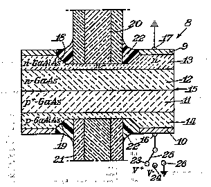
`Reference to Fig. l provides a description of the basic
:s~ructure of the instant inve~tion. ~hown in the drawing, not
to scale, is a cros~ ~ectional view of diode 8 with a heavily
doped active layer ll of p-type gallium argenide (GaAs) of a
doping concentr~t~on o~ about~l0~9 cm'3. Wav~guiding lay~r 12 is
lightly doped n-~ype GaAs, with 2 doping concentration of 1015
~m~ .'3. .. to ~10~6 cm'3. ~ Con~ining l~yer 13 o~ the gailium ~lu~inum
arsenide -(GaAlA~) is doped ~or n-type conduct~v~ty ~t a con-
~entration of the order of l018 cm3 whlle layer 14 also GaAlAs
is:aop~d p-type~at a~ ilar concentration. ~è~erence is made
to the de~cription~1n'U.S. ~pp1ication Serl~1 Nu=bër 07i247,042
,
"~ , .
., " " ~ ,
.: .. . ~ . , ,, :
: . .
,, ,, . , , ,. ~ .
, ;
WO91/12633 2 0 7 ~ 3 ~ ~: PCT/~S91/006~
of the lightly doped n-type layer, al~o referred to as the
w~veguiding layer, and of the more highly doped p-type layer,
also referred to a~ the active layer. When the diode is re-
versed biased for th~ detecting mode of operation, the lightly
doped layer will be mostly depleted. This feature helps the
function of the depletion layer in the detection ~ode.
P n junction 15 is formed between layers ll and 12.
Metallizations 9 and lO are provided on the exterior of the
layers 13 and l~ respec~ivelyO Electrode 16 is applied to
metallization lO and ground contact ~7 to m@tallization 9 for
appllcation of voltage for operation as an emitter-or detector.
Wells 18 and l9 are formed respectively in layers 13 and 14
receiving directly-coupled optical waveguide elements, herein-
after referred to as optical fi~ers 20 and ~l, respec~ively.
The ~ibers 20 and 21 are secured in ~he respective wells 18 a~d
l9 by a suitable cement 22. A switch 25 is attached to electr-
ode 16 has a position 23 providing a rorward bias-for ~he
emitter mode and a position 24 for the receiver mode and a
neutral position 26.
This device is particularly advantageou with multi-mode-
core sized optical fibers, and it is a ~eature that when the
de~ice is quiescent or in the off position 26, a ~i~nal will
pass thro~gh with iow loss. . ..
-~~ In the diode device of this-invention,1ight ~s referred to
herein includes wavelengths in the optic~l . æpectrum ~utside ~f
the narrow band to which the human eye i ~ensitive i.e. 400 nm
to 700 nm. ; While for the purpo~e o~ the description of .an~
embodiment the spectrum associated.with gallium arsenide is
referred to, ~ will bè readily understood,by tho~e ~killed in
the art that the pre~ent invention can be. carri~d out .with -other .
' ,. - : : ,, ', ' :.
,, .: . . : , : .; : , . ' .
.. : ' ,: ' , ' ' '' ~ :
WO91tl2633 2 0 7 ~ 3:~ 8 PCT/US91/006~ f
8 i;
semicondu~ting materials to operate at other ranges of wave-
lengths. For example with gallium indium arsenide phosphide, it
would be effective at longer wavelengths up to l.7 micrometers.
In the surface-oriented devices o~ this invention light may
be received ~rom either direction normal ko the p-n junction and
absorbed in the lightly doped n-type wave guiding layer. The
resultant detec~ion takes place in the depletion region in this
waveguiding layer under reversé biasing. For light emission, a
forward bias causes electron injection into the heavily doped p-
type active layer leading to recombination in which the electron
gives up energy to produce photon~. The quantum efficiency is
as defined above. The bi-directional operation of the devices
of this invention includes an ampfication mode under forward
bias. When forward biased with small DC voltage the structure
of the present invention amplifies signals fed through from one
optical fiber to`another. However at the present state of the
art using this device as an amplifier may havs certain draw-
backs.
Fig. 2 and 3 illustrate structures which are adjusted to
improve emission of the light by confining the current to the
center of the diode structure.
Fig. 2 illustrates the preferred e~bodiment ~f the bi-
directional structure 27 which is designed to provide mechanical
stability with gallium~arsènide ~layërs 28 and 29 ~o provide
strength and-'low resistance ~or electrical contact. In the
diode`27 a-p-n junction-30 is formed between a lightly doped n~
type~gallium ~arsenide-layer 31 of 1-3 ~m in thickness and a
heavilyidoped p-type` gàilium arsenide layer 32 of O.S ~m ln
thickness.i~ -A~joining -layér~33 is a p-type` gallium aluminum
arsenide~confining layex.- An n-typè gallium aluminum arsenide
: : - .: , , . ~ : , ,
:,
::,: , . . :
- , ~ - ~ ,. , . ., :
W091/12633 2 ~ 7 ~;3 ~ 8 pcT/us91/oo6~
~; .
confining layer 34 adjoins layer 31 and i~ l.O ~m thick. L~yers
33 and 34 are doped with concentrations o~ 1018cm 3, n-type and p-
type respectively. A heavily-doped n region 35 is centrally
incorporated in layer 34 and of a diameter of 50-75 ~m. A
imilar sized heavily-doped p~ region 36 may also be added to
layer 33. The r~gions 35 and 36 concentrats the recombi~ation
and emission of ligh~ centrally of the diode 27 and concentric
with wells 37 and 38 form~d in the respective upport layers 28
and 29. Optical fibers 39 and 40 are ~urface-oriented in
coupling position in the respective well~ 37 and 38. The fib rs
39 and 40 are secured in their respective wells 37 and 38 by a
cement 41. The centrally positioned regions 35 and 36 create
easy paths for carriers to follow and accordingly improve the
quantum efficiency in the operation of the emitt~r mode. In
this embodiment the wells 37 and 38 have a diameter of ~rom 150
- 200 ~m. The diode 27 is provided with metallizations 42 and
3 for electrical connections and operation as described above
in relation to the structure illustrated Fig 1. A 6witc~ 25B
selectively connects positions 23B,-24B and 26B to the diode at
electrode 16B. The height of the diode 27-from metallization
42 to metallization 43 is in the range from 150 to 200 ~m.
Fig. 3 illustrates a modification of the invention having
a..diode 45 which has a sio2 support l~yer 46 and support layer 47
of n-type gallium~arsenide with:weils 48 and 49 formed in the
respective.layers 46 and 47. The diode 45 ha~ a p-n junction 50
formed between a lightly doped n-type-l~yer 51 and a heavily
doped p-type layer'52?of gallium ars~nide. -Confining layers 53
and 54~are respectively-n-type/conductivity and p-type conduc-
tivity..yallium aluminum`arsenide. i Structural; strength is
provided by the layers 46~ànd 47,-whiië-thé windows~~for light
. - ; , ~ . ~ , . ........................ . . . .
,", ," , . .
, . , . ,; , ,.,. , ., .: :; ,
,'~ " 1 ` ' i . '
WO91/12633 2 0 7 .j 3 ~ 8 1 o PCT/US91/~0684 ~
transmission are provided by the well~ 48 and 49 in which
optical fibers 55 and 56 ars arranged ~o as to be ~urface-
oriented with thelr axes normal to the plane of the p-n junction
50. The diode 45 is provided with metallizations 57 and 58 for
ele~ctrical connection and operation through electrcde 16C,
ground contact 17C, switch 25C and positions 23C, 24C and 26C in
... . .. . .
the same manner as ~he switching arrangement described above for
Fig. l.
A region 60 of higher n-~ype concentration, 1019cm3 is
centrally positioned in layer 53, which provides increased
efficiency of ligh~ emission by directing current to the central
region of the diode 45. ~ hea~ ~ink 59 is in contact with
metallization 58 to dissip~te heat and improve the diode's
efficiency.
Figs. 4 and 5 illustrate o~her modifications in the unitary
emitter-detector.diode according to this invention. The modifi-
cation is provided at the ends of the optical fibers at the
diode. In Fig. 4 a spherical lens provides direct coupling
between th~ fiber and the diode at the parallel sur~ace of the
diode. In Fig. 5 the tip of the optical fiber is modified. In
both Figs. 4 and 5 a diode 61 has confining layers 62 and 63 of
p-type & n-type conducti~ity respectively a p-type active layer
64 forms a p-n junction 65 with an n-type layer 66. Support
layers 67 and 68 are formed with wells 69 and 70 to bring:the
.. . ... ... ., . , . ~ . ... .. . . .
parallel lateral surfaces ?1 and 72 of the wells nearer to the
p-n ~unction 65.. Optical fibers~73 and 7~ are positioned.with
their axe~;normal to the junction 65 at the-~respective wells ~9
and 70 at each ~ide of the.diode 61. In the Fig. 4 embodiment
`~ . s :-, ` .. J _ . v . ` - - `
the wells 69 and 70 each contain a ~pherical glass ball lens 75
cemented~in the respective well~69 or 70.;;The fibers 73 and-74
:
-
" ' '` " ' ~ ": '`'~ ., ~ ., ~,,
.. ..
WO91/12633 2 0 7 ~ 3 ~ 8 PCT/USgl/006~
are csmented ~o the diode 61 so that they t~rminate at th~lenses 75. It will be understood that the transmitted light
passing through the fibers 73 and 74 is focussed by passage
through the lenses 75 which are of lesser diameter than th~
fibers 73 and 74. The efficiency cf the transmission and
~oupling is accordingly improved..
In Fig. ~ optical fibers 76 and 77 terminate at the
parallel~surfaces 71 and 72 in elliptical fiber tips 78 and 79.
The tips 78 and 79 are cemented within the wells 69 and 70 with
the fiber axes normal ~o the p-n junction 65 to draw the ~low of
ph~tons centrally o~.the diode.
As seen ~rom the preferred embodiment of Fig. 2, the diode
27 provides a reduction in the spread of the current within the
diode during its operation. This invention brings the waveguid-
ing means, for example ~he optical fibers, close to the active
volume of the diode and also brings the ends of the ~ibers close
together. ~urther the diode of this invention guides and
concentrates the photon emission within the diode. The effect
is ~xemplified by the illustrated embodiments for example as in
Fig. 2, when a forward bias is applied at 23, co~tinuous or
pulsed, light is emi~ted from the active volume. The active
volume is defined as the regio~ directly below the optical fi~er
and is further defined by the diameter of regions 35 and 36.
Light from this region is produced by the recombination of
electrons from the co~duction band with holes in ~he valence
band. This reco~bination results in the e~ission of a photon
with energy E=h . Because regions 35 and 36 will reduce the
amount of current spreading across diode 27, a large percentage
9f that photon e~ission will occur within the active volume, and
directly below fiber 39 and 40. Light from thi~ region is
.
. .
WO91/12633 20 ~ PCT/US91/006~
12 ~,
emitted in a Lambertian pattern, thu~ ~ome photons are absorbed
within the ~iode and other photons are simply lost, however, a
good approximation of the light coupled into the fiber is given
.by (NA)2 where DF is the diameter of the fiber, DE is the
diameter of the emission region and NA is the numerical aperture
of the fiber. Also, shown in Fig.- 4 and fig.5 are methods for
increasing the amoun~.of light coupled into the ~iber.
As changes could be made in the above described embodiment
of this invention without departing ~rom the scope of the
claims, it is intended that the above description is illustra-
tivP and having thus described our invention, what we claim as
new and desire to secure by Letters Patent of the United States
is:
- . ,,
. . ~. .- . i ,; ...,,: - -
.,. .. : ,.. ,~ ~ , . . . ..
;~
:~'
~ "
;~
~ : , "
, ' '', ', ' ' ' ~ . ,.~ ' ~:,' ' .
:,,:,: : , . : ,, , ~