Note: Descriptions are shown in the official language in which they were submitted.
2~7~783
-1- P-257
HIGH DENSITY INK JET PRINTHEAD
BACKGROUND OF THE INVENTION
Field of the Invention
The invention relates to a high density ink
jet printhead and, more particularly, to a multiple
channel, sidewall actuated high density ink jet
printhead configured for cross-talk reduced
operation.
Description of Related Art
Printers provide a means of outputting a
permanent record in human readable form.
Typically, a printing technique may be categorized
as either impact printing or non-impact printing.
In impact printing, an image is formed by striking
an inked ribbon placed near the surface of the
paper. Impact printing techniques may be further
characterized as either formed-character printing
or matrix printing. In formed-character printing,
the element which strikes the ribbon to produce the
image consists of a raised mirror image of the
- ~ red character. In matrix printing, the
, ,. "',.1 ~,~,?
- character is formed as a series of closely spaced
dots which are produced by striking a provided wire
or wires against the ribbon. Here, characters are
. 2~5~83
-2- P-257
formed as a series of closely spaced dots produced
by striking the provided wire or wires against the
ribbon. By selectively striking the provided
wires, any character representable by a matrix of
d~t~ can be produced.
Non-impact printing is often preferred over
impact printing ~n view of its tendency to provide
higher printing speeds as well as its better
suitability for printing graphics and half-tone
images. Non-impact printing techniques include
matrix, electrostatic and electrophotographic type
printing techniques. In matrix type printing,
wires are selectively heated by electrical pulses
and the heat thereby generated causes a mark to
appear on a sheet of paper, usually specially
treated paper. In electrostatic type printing, an
electric arc between the printing element and the
conductive paper removes an opaque coating on the
paper to expose a sublayer of a contrasting color.
Finally, in electrophotographic printing, a
photoconductive material is selectively charged
utilizing a light source such as a laser. A powder
toner is attracted to the charged regions and, when
placed in contact with a sheet of paper, transfers
to the paper's surface. The toner is then
subjected to heat which fuses it to the paper.
Another form of non-impact printing is
generally classified as ink jet printing. Ink jet
printing systems use the ejection of tiny droplets
of ink to produce an image. The devices produce
highly reproducible and controllable droplets, so
that a droplet may be printed at a location
specified by digitally stored image datac Most ink
jet printing systems commercially available may be
generally classified as either a "continuous jet"
23~57~:3
-3- P-257
type ink jet printing system where droplets are
continuously ejected from the printhead and either
directed to or away from the paper depending on the
desired image to be produced or as a "drop on
demand~ type ink jet printing system where droplets
are ejected from the printhead in response to a
specific command related to the image to be
produced.
Continuous jet type ink jet printing systems
are based upon the phenomena of uniform droplet
formation from a stream of liquid issuing from an
orifice. It had been previously observed that
fluid ejected under pressure from an orifice about
50 to 80 microns in diameter tends to break up into
uniform droplets upon the amplification of
capillary waves induced onto the jet, for example,
by an electromechanical device that causes pressure
oscillations to propagate through the fluid. For
example, in FIG. 1, a schematic illustration of a
continuous jet type ink jet printer 200 may now be
seen. Here, a pump 202 pumps ink from an ink
supply 204 to a nozzle assembly 206. The nozzle
assembly 206 includes a piezo crystal 208 which is
continuously driven by an electrical voltage
supplied by a crystal driver 210. The pump 202
forces ink supplied to the nozzle assembly 206 to
be ejected through nozzle 212 in a continuous
stream. The continuously oscillating piezo crystal
208 creates press~re disturbances that cause the
continuous stream of ~nk to break-up into uniform
dr~plets of ink and acquire an electrostatic charge
due to the presence of an electrostatic field,
often referred to as the charging field, generated
by electrodes 214. Using high voltage deflection
plates 216, the trajectory of selected ones of the
2U75~3
-4- P-257
electrostatically charged droplets can be
controlled to hit a desired spot on a sheet of
paper 218. The high voltage deflection plates 216
also deflect unselected ones of the
electrostatically charged droplets away from the
sheet of paper 218 and into a reservoir 220 for
recycling purposes. Due to the small size of the
droplets and the precise trajectory control, the
quality of continuous jet type ink jet printing
systems can approach that of formed-character
impact printing systems. However, one drawback to
continuous jet type ink jet printing systems is
that fluid must be jetting even when little or no
printing is required. This requirement degrades
the ink and decreases reliability of the printing
system.
Due to this drawback, there has been increased
interest in the production of droplets by
electromechanically induced pressure waves. In
this type of system, a volumetric change in the
fluid is induced by the application of a voltage
pulse to a piezoelectric material which is directly
or indirectly coupled to the fluid. This
volumetric change causes pressure/velocity
transients to occur in the fluid and these are
directed so as to produce a droplet that issues
from an orifice. Since the voltage is applied only
when a droplet is desired, these types of ink jet
printing systems are referred to as drop-on-demand.
For example, in FIG. 2, a drop on demand type ink
iet printer is schematically illustrated. A nozzle
assembly 306 draws ink from a reservoir (not
shown). A driver 310 receives character data and
actuates piezoelectric material 308 in response
thereto. For example, if the received character
2~7S~83
-5- P-257
data requires that a droplet of ink is to be
ejected from the nozzle assembly 306, the driver
310 will apply a voltage to the piezoelectric
material 308. The piezoelectric material will then
deform in a manner that will force the nozzle
assembly 306 to eject a droplet of ink from orifice
312. The ejected droplet will then strike a sheet
of paper 318.
The use of piezoelectric materials in ink jet
printers is well known. Host commonly,
piezoelectric material is used in a piezoelectric
transducer by which electric energy is converted
into mechanical energy by applying an electric
field across the material, thereby causing the
piezoelectric material to deform. This ability to
distort piezoelectric material has often been
utilized in order to force the ejection of ink from
the ink-carrying channels of ink jet printers. One
such ink jet printer configuration which utilizes
the distortion of a piezoelectric material to eject
ink includes a tubular piezoelectric transducer
which surrounds an ink-carrying channel. When the
transducer is excited by the application of an
electrical voltage pulse, the ink-carrying channel
is compressed and a drop of ink is ejected from the
channel. For example, an ink jet printer which
utilizes circular transducers may be seen by
reference to U.S. Patent No. 3,857,049 to Zoltan.
However, the relatively complicated arrangement of
the piezoelectric transducer and the associated
ink-carrying channel causes such devices to be
relatively time-consuming and expensive to
manufacture.
In order to reduce the per ink-carrying
channel (or "jetn) manufacturing cost of an ink jet
207~ 3
-6- P-257
printhead, in particular, those ink jet printheads
~a~ing ~ piezoelectric actuator, it has long been
des~red to pro~ce ~n ink jet printhead having a
channel array in which the individual channels
which comprise the array are arranged such that the
spacing between adjacent channels is relatively
small. For example, it would be very desirable to
construct an ink jet printhead having a channel
array where adjacent channels are spaced between
approximately four and eight mils apart. Such a
ink jet printhead is hereby defined as a "high
density" ink jet printhead. In addition to a
reduction in the per ink-carrying channel
manufacturing cost, another advantage which would
result from the manufacture of an ink jet printhead
with a high channel density would be an increase in
printer speed. However, the very close spacing
between channels in the proposed high density ink
jet printhead has long been a major problem in the
manufacture of such printheads.
Recently, the use of shear mode piezoelectric
transducers for ink jet printhead devices have
become more common. For example, U.S. Patent Nos.
4,584,590 and 4,825,227, both to Fischbeck et al.,
disclose shear mode piezoelectric transducers for
a parallel channel array ink jet printhead. In
both of the Fischbeck et al. patents, a series of
open ended parallel ink pressure chambers are
covered with a sh~et o~ a piezoelectric material
alonq t~eir ro~fs. ~lectrodes are provided on
opposite sides of the sheet of piezoelectric
material such that positive electrodes are
positioned above the vertical walls 6eparating
pressure chambers and negative electrodes are
positioned over the chamber itself. When an
20757~3
~7- P-257
electric field is provided across the electrodes,
the piezoelectric material, which is polled in a
direction normal to the electric field direction,
distorts in a shear mode configuration to compress
the ink pressure chamber. In these configurations,
however, much of the piezoelectric material is
inactive. Furthermore, the extent of deformation
of the piezoelectric material is small.
An ink jet printhead having a parallel channel
array and which utilizes piezoelectric materials to
construct the sidewalls of the ink-carrying
channels may be seen by reference to U.S. Patent
No. 4,536,097 to Nilsson. In Nilsson, an ink jet
channel matrix is formed by a series of strips of
a piezoelectric material disposed in spaced
parallel relationships and covered on opposite
sides by first and second plates. One plate is
constructed of a conductive material and forms a
shared electrode for all of the strips of
piezoelectric material. On the other side of the
strips, electrical contacts are used to
electrically connect channel defining pairs of the
strips of piezoelectric material. When a voltage
is applied to the two strips of piezoelectric
material which define a channel, the strips become
narrower and higher such that the enclosed cross-
sectional area of the channel is enlarged and ink
is drawn into the channel. When the voltage is
removed, the strips return to their original shape,
thereby reducing channel volume and ejecting ink
therefrom.
An ink jet printhead having a parallel ink-
carrying channel array and which utilizes
piezoelectric material to form a shear mode
actuator for the vertical walls of the channel has
-8- P-257
also been disclosed. For example, U.S. Patent Nos.
4,879,568 to Bartky et al. and 4,887,100 to
Michaelis et al. each disclose an ink jet printhead
channel array in which a piezoelectric material is
used as the vertical wall along the entire length
of each channel forming the array. In these
configurations, the vertical channel walls are
constructed of two oppositely polled pieces of
piezoelectric material mounted next to each other
and sandwiched between top and bottom walls to form
the ink channels. Once the ink channels are
formed, electrodes are then deposited along the
entire height of the vertical channel wall. When
an electric field normal to the poling direction of
the pieces of piezoelectric material is generated
between the electrodes, the vertical channel wall
distorts to compress the ink jet channel in a shear
mode fashion.
SUMMARY OF THE l~v~NlION
In one embodiment, the present invention is of
an ink jet printhead which comprises a base section
having a series of generally parallel spaced
projections extending longitudinally therealong, a
series of intermediate sections conductively
mounted on a top side of a corresponding one of the
series of base section projections and a top
section conductively mounted to a top side of each
of the series of intermediate sections. The base
section, intermediate sections and top section
define generally parallel, axially extending ink-
carrying channels for the ejection of ink
therefrom. To actuate a channel, a positive
~o~t~ge and negative voltage are selectively
applied to the conductive mounting connecting the
projection and the intermediate section along the
211~S~
-9- P-257
respective sidewalls of the channel while the
conductive mounting connecting the top cover and
the intermediate sections are connected to ground.
In another embodiment, the present invention
is of an ink jet printhead comprised of a generally
U-shaped actuator, a first side actuator having a
bottom wall conductively mounted to a first top
wall of the generally U-shaped actuator, a second
side actuator having a bottom wall conductively
mounted to a second top wall of the generally U-
shaped actuator and a top section having a bottom
wall conductively mounted to the top walls of the
first and second side actuators. Elongated liquid
confining channels are defined by the generally U-
shaped actuator, the first side actuator, the
second side actuator and the top section. The
generally U-shaped actuator, the first side
actuator and the second side actuator are
electrically connected for the selective
application of first, second and third pressure
p~lses, respectively, to the elongated liquid
confining channel.
In yet another embodiment, the present
invention is of an ink jet printhead comprising a
base having at least three generally parallel
elongated liquid confining channel extending
therethrough and a cover having a corresponding
number of apertures formed therein mounted to a
front side of the ~ase. The apertures are
positi~ned on the cover to define first, second,
and third generally parallel aperture rows of at
least one aperture each and to place each one of
the apertures in communication with a corresponding
one of said channels. The channels which
correspond to the first, second or third rows of
20757~3
-10- P-257
apertures, respectively, may be simultaneously
actuated to cause the ejection of ink from the
channels corresponding to those rows.
BRIEF DESCRIPTION OF THE DRAWING
The present invention may be better
understood, and its numerous objects, features and
advantages will become apparent to those skilled in
the art by reference to the accompanying drawing,
in which:
FIG. 1 is a schematic illustration of a
continuous jet type ink jet printhead;
FIG. 2 is a schematic illustration of a drop
on demand type ink jet printhead.
FIG. 3 is a perspective view of a
schematically illustrated ink jet printhead
constructed in accordance with the teachings of the
present invention;
FIG. 4 is an enlarged partial cross-sectional
view of the ink jet printhead of FIG. 3 taken along
lines 4--4 and illustrating a parallel channel
array of the ink jet printhead of FIG. 3;
FIG. 5 is a side elevational view of the ink
jet printhead of FIG. 3;
FIG. 6a is an enlarged partial cross-sectional
view of a rear portion of the ink jet printhead of
FIG. 4 taken along lines 6a--6a;
FIG. 6b is an enlarged partial cross-sectional
view of a rear portion of the ink jet printhead of
FIG. 4 taken along lines 6b--6b;
FIG. 7 is an enlarged partial perspective view
of the rear portion of the ink jet printhead of
FIG. 3 with top body portion removed;
FIG. 8a is a front elevational view of a
single, undeflected, actuator sidewall of the ink
jet printhead of FIG. 3;
207S~83
-11- P-257
FIG. 8~ is a ~ront elevational view of the
single actuator sidewall of FIG. 8a after
deflection;
FIG. 9a is a front view of an alternate
embodiment of the schematically illustrated ink jet
printhead of FIG. 3 with front wall removed and
after deflection of the actuator sidewalls of the
parallel channel array;
FIG. 9b is an enlarged partial front view of
the schematically illustrated ink jet printhead of
FIG. 9a;
FIG. 9c is a graphically illustrated
electrostatic field displacement analysis for the
sidewall configuration of FIG. 9b;
FIG. lOa is a front elevational view of a
second embodiment of the undeflected actuator
sidewall illustrated in FIG. 8a; FIG. lOb is a
front elevational view of the actuator sidewall of
FIG. lOa after deflection;
FIG. lla is a front elevational view of a
third embodiment of the undeflected actuator
sidewall illustrated in FIG. 8a;
FIG. llb is a front elevational view of the
actuator wall of FIG. lla after deflection;
FIG. 12a is a front elevational view of a
fourth embodiment of the undeflected actuator
sidewall illustrated in FIG. 9a;
FIG. 12b is a front elevational view of the
actuator wall of FIG. 12a after deflection;
~IG. 13a is a front elevational view of a
fi~th em~odiment o~ the undeflected actuator wall
illustrated in FIG. 8c;
FIG. 13b is a front elevational view of the
actuator wall of FIG. 13c after deflection; and
FIG. 14 is a partial cross-sectional view of
20 7 57 8 3
- 12 -
another alternate embodiment of the ink jet printhead of FIG.
3 taken along lines 14--14;
FIG. 15a is an enlarged partial front view of yet
another alternate embodiment of the ink ]et printhead of FIG.
3;
FIG. 15b is a second front view of the ink jet
printhead of FIG. 15a with front wall removed and after a
first deflection of a deflection sequence for the actuator
sidewalls of the parallel channel array;
FIG. 15c is the ink jet printhead of FIG. 16b after
a second deflection of the deflection sequence; and
FIG. 15d is the ink jet printhead of FIG. 15b after
a third deflection of the deflection sequence.
DETAILED DESCRIPTION OF A PREFERRED EMBODIMENT
Referring now to the drawing wherein thicknesses and
other dimensions have been exaggerated in the various figures
as deemed necessary for explanatory purposes and wherein like
reference numerals designate the same or similar elements
throughout the several views, in FIG. 3, an ink jet printhead
10 constructed in accordance with the teachings of the present
invention may now be seen. The ink jet printhead 10 includes
a main body portion 12 which is aligned, mated and bonded to
an intermediate body portion 14 which, in turn,
72159-51
~ ~ .
2d7S~3
-13- P-257
is aligned, mated and bonded to a top body portion
16. As will be better seen in FIG. 6a, in the
embodiment of the invention illustrated herein, the
main body portion 12 continues to extend rearwardly
past the intermediate body portion 14 and the top
body portion 16, thereby providing a surface on the
ink jet printhead 10 on which a controller (not
visible in FIG. 3) for the ink jet printhead 10 may
be mounted. It is fully contemplated, however,
that the main body portion 12, the intermediate
body portion 14 and the top body portion 16 may all
be of the same length, thereby requiring that the
controller 50 be remotely positioned with respect
to the ink jet printhead 10.
A plurality of vertical grooves of
predetermined width and depth are formed through
the intermediate body portion 14 and the main body
portion 12 to form a plurality of pressure chambers
or channels 18 (not visible in FIG. 3), thereby
providing a channel array for the ink jet printhead
10. A manifold 22 (also not visible in FIG. 3) in
communication with the channels 18 is formed near
the rear portion of the ink jet printhead 10.
Preferably, the manifold 22 is comprised of a
channel extending through the intermediate body
portion 14 and the top body portion 16 in a
direction generally perpendicular to the channels
18. As to be more fully described below, the
manifold 22 co~municates with an external ink
conduit 46 t~ provide means for supplying ink to
the channels 18 from a source of ink 25 connected
to the external ink conduit 46.
Continuing to refer to FIG. 3, the ink jet
printhead 10 further includes a front wall 20
having a front side 20a, a back side 20b and a
2~7~783
-14- P-257
plurality of tapered orifices 26 extending
therethrough. The back side 20b of the front wall
20 is aligned, mated and bonded with the main,
intermediate and top body portions 12, 14 and 16,
respectively, such that each orifice 26 is in
communication with a corresponding one of the
plurality of channels 18 formed in the intermediate
body portion 14, thereby providing ink ejection
nozzles for the channels 18. Preferably, each
orifice 26 should be positioned such that it is
located at the center of the end of the
corresponding channel 18, thereby providing ink
ejection nozzles for the channels 18. It is
contemplated, however, that the ends of each of the
channels 18 could function as orifices for the
ejection of drops of ink in the printing process
without the necessity of providing the front wall
20 and the orifice 26. It is further contemplated
that the dimensions of the orifice array 27
comprised of the orifices 26 could be varied to
cover various selected lengths along the front wall
20 depending on the channel requirements of the
particular ink jet printhead 10 envisioned. For
example, in one configuration, it is contemplated
that the orifice array 27 would be approximately
0.064 inches in height and approximately 0.193
inches in length and be comprised of about twenty-
eight orifices 26 provided in a staggered
configuration where the centers of adjacent
orifices 26 would be approximately 0.0068 inches
apart.
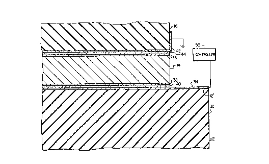
~eferring ne~t to FIG. 4, an enlarged partial
cross-sectional view o~ the ink jet printhead 10
taken along lines 4--4 of ~IG. 3 may now be seen.
As may now be clearly seen, the ink jet printhead
2~75~3
-15- P-257
10 includes a pl~rality of parallel spaced channels
18, each channel 18 vertically extending from the
top body portion 16, along the intermediate body
portion 14 and part of the main body portion 12 and
extending lengthwise through the ink jet printhead
10. The main body portion 12 and the top body
portion 16 are constructed of an inactive material,
for example, unpolarized piezoelectric material.
Separating adjacent channels 18 are sidewall
actuators 28, each of which include a first
sidewall section 30 and a second sidewall section
32. The first sidewall section 30 is constructed
of an inactive material, for example unpolarized
piezoelectric material, and, in the preferred
embodiment of the invention, is integrally formed
with the body portion 12. The second sidewall
section 32, is formed of a piezoelectric material,
for example, lead zirconate titante (or "PZT"),
polarized in direction "pll perpendicular to the
channels 18.
Mounted to the top side of each first sidewall
section 30 is a metallized conductive surface 34,
for example, a strip of metal. Similarly,
metallized conductive surfaces 36 and 38, also
formed of a strip of metal, are mounted to the top
and bottom sides, respectively, of each second
sidewall section 32. A first layer of a conductive
adhesive 40, for example, an epoxy material, is
provided to conductively attach the metallized
conductive surface 34 mounted to the first sidewall
section 30 and the metallized conductive surface 38
mounted to the second sidewall section 32.
Finally, the bottom side of the top body~portion 16
is provided with a metallized conductive surface 42
which, in turn, is conductively mounted to the
2~578~
-16- P-257
metallized conductive surfaces 36 of the second
sidewall section 32 by a second layer of a
conductive adhesive 44. In this manner, a series
of channels 18, each channel being defined by the
unpolarized piezoelectric material of the main body
portion 12 along its bottom, the layer of
conductive adhesive 44 along its top and a pair of
sidewall actuators 28 have been provided. Each
sidewall actuator 28 is shared between adjacent
channels 18. The first sidewall section 30 may be
formed having any number of various heights
relative to the second sidewall section 32. It has
been discovered, however, that a ratio of 1.3 to 1
between the first sidewall section 30 constructed
of unpolled piezoelectric material and the second
sidewall section 32 formed of polarized
piezoelectric material has proven quite
satisfactory in use. Furthermore, while the
embodiment of the invention illustrated in FIG. 4
includes the use of metallized conductive surfaces
34, 36, 38 and 42, it has been discovered that the
use of such surfaces may be omitted without
adversely affecting the practice of the invention.
Referring next to FIG. 5, a side elevational
view of the high density ink jet printhead 10 which
better illustrates the means for supplying ink to
the channels 18 from a source of ink 25 may now be
seen. Ink stored in the ink supply 25 is supplied
via the external ink conduit 46 to an internal ink
conduit 24 which extends vertically through the top
body portion 16. The internal ink conduit 24 may
be positioned anywhere in the top body portion 16
of the ink jet printhead 10 althoug~, in the
preferred embodiment of the invention, the internal
ink conduit 24 extends through the general center
~0~578~
-17- P-257
of the top body portion 16. Ink supplied through
the internal ink conduit 24 is transmitted to a
manifold 22 extending generally perpendicular to
and in communication with each of the channels 18.
The manifold 22 may be formed within the
intermediate body portion 14 or the top body
portion 16, although, in the printhead illustrated
herein, the manifold 22 is formed within the top
body portion 16. While the channels 18 extend
across the entire length of the ink jet printhead
10, a block 48 of a composite material blocks the
back end of the channels 18 so that ink supplied to
the channels 18 shall, upon actuation of the
channel 18, be propagated in the forward direction
where it exits the ink jet printhead 10 through the
corresponding one of the tapered orifices 26.
Referring next to FIG. 6a, a cross-sectional
view of a rear portion of the ink jet printhead 10
taken along lines 6a--6a of FIG. 3 which
illustrates a sidewall of the channel 18 may now be
seen. Also visible here is the electrical
connection of the ink jet printhead 10. A
controller 50, for example, a microprocessor or
other integrated circuit, is electrically connected
to the metallized conductive surface 34 which
separates the first and second sidewall actuator
sections 30, 32. It should be further noted that
while, in the embodiment illustrated in FIG. 6a, a
remotely located controller is disclosed, it is
contemplated that the controller may be mounted on
the rearwardly extending portion 12' of the main
body portion 12. Each metallized conductive
surface 42 which separates the second sidewall
section 32 and the top body portion 16, on the
other hand, is connected to ground. While FIG. 6a
2~75~83
-18- P-257
illustrates the electrical connection of a single
conductive strip 34 to the controller 50 and the
single conductive strip 42 to ground, it should be
clearly understood that each sidewall actuator 30
has a similarly constructed conductive strip 34
extending outwardly at the rear portion of the ink
jet printhead 10 for connection to the controller
5~ and a similarly constructed conductive strip 42
connected to ground. As to be more fully described
below, the controller 50 operates the ink jet
printhead 10 by transmitting a series of positive
and/or negative charges to selected ones the
conductive strips 34. As the top body portion 16
and main body portion 12 are non-conductive and
layer of adhesive material 40, conductive
metallized surface 38, intermediate body portion
14, conductive metallized surface 36, layer of
adhesive material 44 and conductive metallized
surface 42 are all conductive, a voltage drop
across the intermediate body portions 14
corresponding to the selected metallized conductive
surfaces 34 will be produced. This will cause the
sidewalls which includes the intermediate body
portion 14 across which a voltage drop has been
placed to deform in a certain direction. Thus, by
selectively placing selected voltages on the
various sidewall actuators, the channels 18 may be
selectively "fired", i.e., caused to eject ink, in
a given pattern, thereby producing a desired image.
The exact configuration of a pulse sequence
for selectively firing the channels 18 may be
varied without departing from the teachings of the
presen~ invention. For ex~mple, a suitable pulse
sequence may be seen by reference to the article to
Wallace, David B., entitled "A Method of
207S783
-19- P-257
Characteristic Model of a Drop-on-Demand Ink-Jet
Device Using an Integral Method Drop Formation
Model", 89-WA/FE-4 (1989). In its most general
sense, the pulse sequence for a sidewall actuator
28 consists of a positive (or "+") segment which
imparts a pressure pulse into the channel 18 being
fired by that sidewall actuator 28 and a negative
(or "-") segment which imparts a complementary,
additive pressure pulse into the channel 18
adjacent to the channel 18 being fired which shares
the common sidewall 28 being actuated. For
example, in one embodiment of the invention, each
sidewall actuator 28 of the pair of adjacent
sidewall actuators 28 which define a channel 18 has
a pulse sequence which includes the aforementioned
positive and negative voltage segments, but for
which the positive and negative voltage segments
are applied during opposing time intervals for
respective ones of the pair, thereby forming a +, -
, +, - voltage pattern which would cause every
other channel 18 to eject a droplet of ink after
the application of voltage. In a second embodiment
of the invention, a first pair of adjacent sidewall
actuators 28 which define a first channel may have
a pulse sequence which includes the aforementioned
positive and negative voltage segments applied
during opposing time intervals for respective ones
of the first pair, and a second pair of adjacent
sidewall actuators 28 which define a second channel
adjacent to the first channel may have no voltage
applied thereto during these time intervals,
thereby forming a ~, -, 0, 0 voltage pattern in
vhich every fourth channel 18 would fire after the
application of voltage. As may be further seen,
multiple patterns of channel actuations too
2075783
-20- P-257
numerous to mention may be provided by the
selective application of voltages to the first
layer of conductive adhesive 40 corresponding to
each sidewall actuator 28.
Referring next to FIG. 6b, a cross-sectional
view o~ the rear portion of the ink jet printhead
10 taken along lines 6b--6b which better
illustrates the ink supply path to the channel 18
via the internal ink conduit and the manifold 22.
Also more clearly visible in FIG. 6b is the block
48, typically formed of an insulative composite
material, which blocks the back end of the channel
18 so that ink supplied to the channel 18 will be
propagated forward upon the activation of a
pressure pulse in a manner more fully described
elsewhere.
Referring next to FIG. 7, the rear portion of
the ink jet printhead with the top body portion 16
and the block of composite material 48 removed is
now illustrated to more clearly show the details of
the structure of the high density ink jet printhead
10. As may be seen herein, in the forming of
channels 18, preferably by sawing the main body
portion 12 and attached intermediate body portion
14 in predetermined locations, portions of the
metallized conductive surfaces 34 are removed,
thereby permitting the metallized conductive
surfaces 34 to function as individual electrical
contact for each sidewall 30 and portions of
metallized conductive surfaces 36 are permitted to
function as individual ground connections for each
sidewall 30.
Referring next to FIG. 8a, a single actuator
wall of the ink jet printhead 10 may now be seen.
The sidewall actuator 28 is comprised of a first
20~57~3
-21- P-257
actuator sidewall section 30 and a second actuator
sidewall section 32, both of which extend along the
entire length of an adjacent channel 18. The first
sidewall section 30 is formed of unpolarized
piezoelectric material integrally formed with the
main body portion 12 of the ink jet printhead 10.
The second sidewall section 32 is formed of a
piezoelectric material poled in a direction
perpendicular to the adjacent channel 18 and is
conductively mounted to the top body portion 16 of
the high-density ink jet printhead 10 which, as
previously set forth, is also formed of an
unpolarized piezoelectric material. The first and
second actuator sidewall sections 30, 32 are
conductively mounted to each other. For example,
the first and second sidewall sections 30, 32 may
be provided with a layer of conductive material 34,
38, respectively, bonded together by a layer of a
conductive adhesive 40. Finally, the top side of
the second actuator sidewall 32 is conductively
mounted to the top body portion 16. by
conductively mounting the metallized conductive
surfaces 36, 42.
Referring next to FIG. 8b, the deformation of
the actuator wall illustrated in FIG. 8a when an
electric field is applied between the metallized
conductive surfaces 34 and 42, shall now be
described in detail. When a selected voltage is
supplied to the metallized conductive surface 34,
an electric field normal to the direction of
polarization is produced. The second sidewall
section 32 will then attempt to undergo shear
deformation. However, as the metallized ~onductive
surface 36 of the second sidewall section 32 is
restrained, the metallized conductive surface 38
20~5~3
-22- P-257
will ~o~e in ~ s~a~ ~otion whi~e the metallized
conductive surface 36 remains fixed. The first
sidewall section 30, being formed of an inactive
material, is unaffected by the electric field.
However, since the first sidewall section 30 is
mounted to the second sidewall section 32
undergoing shear deformation, the first sidewall
section 30 will be pulled by the second sidewall
section 32, thereby forcing the first sidewall
section 30 to bend in what is hereby defined as a
"shear-like motionn. This motion by the sidewall
28 produces a pressure pulse which increases the
pressure in one of the adjacent channels 18
partially defined thereby to cause the ejection of
a droplet of ink from that channel 18 shortly
thereafter and a reinforcing pressure pulse in the
other one of the adjacent channels 18.
Referring next to FIG. 9a, the typical
operation of an alternate embodiment of the channel
array of the high density ink jet printhead 10
subject of the present application will now be
described. In this embodiment of the invention,
the metallized conductive surfaces 34 and 38 and
the layer of conductive adhesive 40 have been
replaced by a sinqle layer of conductive adhesive
51. Similarly, the metallized conductive surfaces
36 and 42 and the layer of conductive adhesive 44
have ~een repl~ced ~y a single layer of conductive
adhes~ve 52. However, in order to eliminate the
aforementioned metallized conductive surfaces while
maintaining satisfactory operation of the high
density ink jet printhead 10, a surface 14b of the
intermediate body portion 14 and a surface 12a of
the main body portion 12 must be conductively
mounted together in a manner such that a voltage
2~7~7~3
-23- P-257
may be readily applied to the single layer of
conductive adhesive 51 and a surface 14a of the
intermediate body portion 14 and a surface 16a of
the top body portion 16 must be conductively
mounted together in a manner such that the single
layer of conductive adhesive 52 therebetween may be
readily connected to ground.
To activate the ink jet printhead 10, the
controller 51 (not shown in FIG. 9a) responds to an
input image signal representative of the image
desired to be printed and applies voltages of
predetermined magnitude and polarity to selected
layers of conductive adhesive 51 which correspond
to certain ones of the actuator sidewalls 28 on
each side of the channels 18 to be activated. For
example, if a positive voltage is applied to a
layer of conductive adhesive 51, then an electric
field E perpendicular to the direction of
polarization is established in the direction from
the layer of conductive adhesive 51 towards the
layer of conductive adhesive 52 and the second
sidewall section 32 will distort in a shear motion
in a first direction normal to the channel 18 while
carrying the first sidewall section 30, thereby
cause the sidewall to undergo a shear-like
distortion. On the other hand, by applying a
negative voltage at the contact 34, the direction
of the electric field E is reversed and the second
sidewall section 32 will deflect in a shear motion
in a ~cond direction~ opposite to the first
direction, and normal to t~e channel 18. Thus, by
placing equal charges of opposite polarity on
adjacent sidewalls which define a channel 18
therebetween, a positive pressure wave is created
in the channel 18 between the two adjacent
~0757~3
-24- P-257
sidewalls and a drop of ink is expelled, either
through the open end 28 of the pressure chamber 18
or through the tapered orifice 26.
Referring next to FIG. 9b, an enlarged view of
a pair of sidewall actuators 28 and a single
channel 18 of the channel array of FIG. 9a in an
unactivated mode may now be seen. As the sidewall
actuators 28 illustrated here are identical in
construction to those described with respect to
FIG. 9a, further description is not necessary.
Prior to activation of the sidewall actuators 28,
the channels 18 were filled with a nonconductive
ink. The piezoelectric material used to form the
sidewall actuators had a relative permittivity of
3300 and the nonconductive ink a relative
permittivity of 1. Two separate tests were
conducted using this embodiment of the invention,
the first test having every fourth channel 18
activated by applying a voltage pattern of (plus,
minus, zero, zero,... ) and the second test having
every other channel 18 activated by applying a
voltage pattern of (plus, minus, plus, minus....).
As no significant differences were produced between
the two tests, only the results of the second test
is described below. In this test, the layer of
conductive material 52 was held at zero volts, the
layer of conductive material 51a was held at plus
1.0 volts, and the layer of conductive material 51b
was held at minus 1.0 volts. Such a voltage
configuration would cause the center channel 18' to
compress.
Referring next to FIG. 9c, a graphical
analysis of the electrostatic field-generated
during activation of the sidewall actuators 28 in
accordance with the parameters of the second test
2075783
-25- P-257
may now be seen. As may be seen here, the
displacement in the polarized piezoelectric
material was of a magnitude such that tooth-to-
tooth and jet-to-jet cross talk effects are
negligible for nonconductive inks. One unexpected
result was that the magnitude electric field in the
unpolarized piezoelectric material was over sixty
percent of that of the poled piezoelectric
material. This phenomena occurred because the flow
of charge is dominated by the high permittivity of
the piezoelectric material. In addition, the
direction of the field in the unpolarized
piezoelectric material is such that, if this
material were polarized, the displacement of the
tooth would increase by greater than sixty percent
due to the unpolarized section of the tooth being
longer than the polarized section. Thus, if the
longer, piezoelectric material piece were
polarized, the displacement would be still greater.
Although not illustrated herein, similar tests
were performed using a conductive inks. In such a
test, the conductive ink would short the layers of
conductive material 51, 52 unless the sidewall
actuators 28 are insulated by a thin layer of
conductive material along the surface of the
sidewall actuators adjacent the channels filled
with conductive ink. It is contemplated,
therefore, that the interior of the channel be
coated with a layer of dielectric material having
a generally uniform thickness of between
approximately 2 and 10 micrometers when the use of
a conductive ink is contemplated. Apart from the
requirement of a layer of dielectric material, the
operation of the ink jet printhead 10 did not
differ significantly when a conductive ink was
207~783
-26- P-257
utilized.
Referring next to FIG. lOa, a second
embodiment of the sidewall actuator 28 may now be
seen. This embodiment is comprised of a first
sidewall section 30 formed of unpolarized
piezoelectric material and integrally formed with
and extending from the main body portion 12, a
second sidewall section 54 formed of a
piezoelectric material and a third sidewall section
56 also constructed of a piezoelectric material.
The second and third sidewall sections 54, 56
should be bonded together such that the poling
directions are rotated 180 degrees from each other.
Each poled piezoelectric material sidewall section
54, 56 should have top and bottom metal layers of
metallized material 57 and 58, 60 and 62,
respectively. The first metallized conductive
surface 57 of the second sidewall section 54 is
mounted to the metallized conductive surface 34 of
the first sidewall section 30 by the first layer of
conductive adhesive 40 and the second metallized
conductive surface 58 of the second sidewall
section 54 is mounted to the first metallized
conductive surface 60 of the third sidewall section
56 by a third layer of conductive adhesive 64.
Finally, the second metallized conductive surface
62 of the third sidewall section 56 is mounted to
the top body portion 16 by the second layer of
conductive adhesive 44. Conductive surface S8 and
conductive surface 38 should be interconnected and
held at common potential, common i.e., ground. An
electric field is created by applying a voltage to
the conductive surface between the second and third
sidewall sections 54, 56. As may be seen in FIG.
lOb, the deformation of the sidewall actuator does
2i~75~'83
-27- P-257
not differ significantly from that previously
described except that each section 54, 56 undergo
individual shear deformations.
Referring next to FIG. lla, the third
embodiment of the sidewall actuator 28 shall now be
described in greater detail. More specifically,
in this embodiment, the first and second sidewall
sections are both constructed of poled
piezoelectric materials such that the direction of
poling are aligned. An electric field is created
by applyinq a voltage to the surface between the
two poled piezoelectric material sections 30, 32.
The electric field vector for the top sidewall
section 32 is 180 degrees relative to that of the
first sidewall section 30. Accordingly, the top
and bottom sidewall sections shear in opposite
directions. However, less than half the voltage
should be needed to achieve the same displacement.
Here, the sidewall actuator is again comprised of
a pair of sidewall sections, but here, the first
and second sidewall sections 66, 68, having first
and second metallized conductive surfaces 70 and
72, 74 and 76, respectively, are both formed of an
active material. Here, the first layer of
conductive adhesive 40 conductively mounts the
first metallized conductive surface 34 of the main
body portion 12 to the first metallized conductive
surface 70 of the first sidewall section 66, a
fourth layer of conductive adhesive 78 conductively
mounts the second metallized conductive surface 72
of the first sidewall section 66 and the first
metallized conductive surface 74 of the second
sidewall section 68, and the second~ layer of
conductive adhesive 44 conductively mounts the
second metallized conductive surface 76 of the
2075783
-28- P-257
second sidewall section 68 and the metallized
conductive surface 42 of the top body portion 16.
As illustrated in FIG. llb, however, in this
embodiment of the invention, both sidewall sections
68, 70 undergo individual shear deformations.
Referring next to FIG. 12a, the fourth
embodiment of the sidewall actuator 28 shall now be
described in greater detail. Here, the sidewall
actuator 28 is comprised of a first sidewall
section 30 formed from an inactive material and
second, third, and fourth sidewall sections 80, 82
and 84 formed from an active material. Each active
sidewall section 80, 82 and 84 has first and second
metallized conductive surfaces 86 and 88, 90 and
92, and 94 and 96, respectively. In this
embodiment, the first layer of conductive adhesive
layer 40 conductively mounts the metallized
conductive surfaces 34 and 86, a third conductive
adhesive layer 98 conductively mounts metallized
conductive surfaces 88 and 90, a fourth conductive
adhesive layer 100 conductively mounts metallized
conductive surfaces 92 and 94, and the second
conductive adhesive layer 44 conductively mounts
metallized conductive surfaces 96 and 42. As may
be seen in FIG. 12b, the deformation is similar to
that illustrated and described with respect to FIG.
8b.
Referring next to FIG. 13a, the fifth
embodiment of the sidewall actuator 28 shall now be
descri~ed in greater detail. Here, the sidewall
actuator 28 is comprised of first, second, third,
fourth, fifth, and sixth sidewall sections 104,
106, 108, 110, 112, and 114, each formed of an
active material and each having first and second
metallized conductive surfaces 116 and 118, 120 and
2075 ;?83
-29- P-257
124, 126 and 128, 130 and 132, 134 and 136, 138 and
140, respectively attached thereto. The first
conductive adhesive layer 40 conductively mounts
metallized conductive surfaces 34 and 116, a third
conductive adhesive layer 142 conductively mounts
~et~lized conductive surfaces layers 118 and 120,
a fourth conductive adhesive layer 144 conductively
mounts metallized conductive surfaces 124 and 126,
a fifth conductive adhesive layer 146 conductively
mounts metallized conductive surfaces 128 and 130,
a sixth conductive adhesive layer 148 conductively
mounts metallized conductive surfaces 132 and 134,
a seventh conductive adhesive layer 150
conductively mounts layers 136 and 138, and the
second conductive adhesive layer 44 conductively
mounts the metallized conductive surfaces 140 and
42. As may be seen in FIG. 13b, the deformation of
the sidewall actuator 28 set forth in this
embodiment of the invention is similar to that
described and illustrated in FIG. llb.
Referring next to FIG. 14, yet another
embodiment of the invention may now be seen. In
this embodiment of the invention, the ink jet
printhead 410 is formed from an intermediate body
portion 414 constructed identically to the
intermediate body portion 14 mated and bonded to a
main body portion 412. As before, the intermediate
body portion 414 is constructed of piezoelectric
material polarized in direction P and has
~e~all~2ed c~cti~e surfaces 436, 438 provided on
surfaces 414b, 414a, respectively. In this
embodiment of the invention, however, the main body
portion 412 is also formed of a pie20electric
material polarized in direction P and has a surface
412a upon which a layer of conductive material 434
2075783
_30- P-257
is deposited thereon. The intermediate body
portion 4~4 and the main body portion 412 are
bonded together by a layer of conductive adhesive
440 which conductively mounts the metallized
conductive surface 434 of the main body portion 412
and the metallized conductive surface 438 of the
intermediate body portion 414 together.
Alternately, bonding between the metallized
conductive surface 434 of the main body portion 412
and the metallized conductive surface 438 of the
intermediate body portion 414 may be achieved by
soldering the metallized conductive surfaces 434,
438 to each other. It is further contemplated
that, in accordance with one aspect of the
invention, one or both of the metallized conductive
surfaces 434 and/or 438 may be eliminated while
maintaining satisfactory operation of the
nventlon .
After the main body portion 412 and the
intermediate body portion 414 are conductively
mounted together, a machining process is then
utilized to form a channel array for the ink jet
printhead 410. As may be seen in FIG. 14, a series
of axially extending, substantially parallel
channels 418 are formed by machining grooves which
extend through the intermediate body portion 414
and the main body portion 412. Preferably, the
machining process should be performed such that
each channel 418 formed thereby should extend
downwardly such that the metallized conductive
surface 436, the intermediate body portion 414 of
polarized piezoelectric material, the metallized
conductive surface 438, the layer of ronductive
adhesive 440, the metallized conductive surface 434
and a portion of the main body portion 412 of
207~783
-31- P-257
polarized piezoelectric material are removed.
In this manner, the channels 418 which
comprise the channel array for the ink jet
printhead and sidewall actuators 428, each having
a first, sidewall actuator section 430 and a second
sidewall actuator section 432, which define the
sides of the channels 418 are formed. As to be
more fully described below, by forming the parallel
channel array in the manner herein described, a
generally U-shaped sidewall actuator 450
(illustrated in phantom in FIG. 14) which comprises
the first sidewall actuator sections 430 on
opposite sides of a channel 418 and a part of the
main body portion 412 which interconnects the first
sidewall actuator sections 430 on opposite sides of
the channel 418 is provided for each of the
channels 418.
Continuing to refer to FIG. 14, the channel
array for the ink jet printhead is formed by
conductively mounting a third block 416 of
unpolarized piezoelectric material, or other
inactive material, having a single layer of
metallized conductive surface 442 formed on the
bottom surface 416a thereof to the metallized
conductive surface 436 of the intermediate body
portion 414. The third block 416, which hereafter
shall be referred to as the top body portion 416 of
the ink ~et printhead, may be constructed in a
manner similar to that previously described with
respect to the top body portion 16. To complete
assembly of the channel array for the ink jet
printhead, the metallized conductive surface 442 of
the top body portion 416 is conductively mounted to
the metallized conductive surface 436 of the second
sidewall section 432 by a second layer of
2075783
-32- P-257
conductive adhesive 444. Preferably, the layer of
conductive adhesive 444 should be spread over the
metallized conductive surface 42 and the top body
portion 416 then be placed onto the metallized
conductive surface 436. As before, it is
contemplated that, in one embodiment of the
invention, either one or both of the metallized
conductive surfaces 436 or 442 may be eliminated
while maintaining satisfactory operation of the
high density ink jet printhead.
To electrically connect the parallel channel
array illustrated in FIG. 14 such that a generally
U-shaped actuator 450 is provided for each of said
channels 418, a electrical contact 452, which, in
alternate embodiments of the invention may be the
metallized conductive surfaces 436 and 438
conductively mounted to each other by the
conductive adhesive 440, the metallized conductive
surfaces 436 and 438 soldered to each other, or a
single layer of conductive adhesive which attaches
surfaces 412a and 414a to each other, on one side
of the channel 418 is connected to +1 V. voltage
source (not shown). A second electrical contact
454 is then connected to a -1 V. voltage source.
To complete the electrical connections for the
parallel channel array, the layer of conductive
adhesive 444 is connected to ground. In this
manner, the channel 18 shall have a generally U-
shaped actuator 450 having a 2 V. voltage drop
between the contact 452 and the contact 454, a
first sidewall actuator having a +l V. voltage drop
betw~en the contact 452 and ground, and a second
sidewall actuator having a -1 V. vol~age drop
between the contact 454 and ground. Once
constructed in this manner, when a +, -, +, -
207~7~3
-33- P-257
voltage pattern is applied to the contacts 40S to
cause every other channel 418 to eject a droplet of
ink upon the application of voltage, significantly
greater compressive and/or expansive forces on the
cha~nel 418 are produced by the combination U-
shaped actuator 450 and the pair of sidewall
actuators 432 that border the channel 418 than that
exerted on the channel 18 by the sidewall actuators
28.
While the dimensions of a high density ink jet
printhead having a parallel channel array with a U-
shaped actuator for each channel may be readily
varied without departing from the scope of the
present invention, it is specifically contemplated
that an ink jet printhead which embodies the
present invention may be constructed to have the
following dimensions:
Orifice Diameter: 40 um
PZT length: 15 mm
PZT height: 120 um
Channel height: 356 um
Channel width: 91 um
Sidewall width: 81 um
In the embodiments of the invention described
above, each sidewall actuator 30 is shared between
a pair of adjacent channels 18 and may be used,
therefore, to cause the ejection of ink from either
one of the channel pair. For example, in FIG. 9a,
every other channel l~a is bein~ fired by
disp~ac n~ ~t~ si~e~ll actuators 30 which form
the sidewalls for the fired channels 18a such that
those channels are compressed. The channels 18b
adjacent to the fired channels 18a remai-n unfired.
However, as each sidewall actuator 30 is shared
between a fired channel 18a and an unfired channel
2~7S7~3
~34- P-257
18b, the sidewall actuators 30 which form the
sidewalls for the unfired channels 18b, are also
displaced, although not in an manner which would
cause the ejection of ink therefrom. The pressure
pulse produced in the unfired channels 18b by the
displacement of the sidewall actuators 30 necessary
to actuate the fired channels 18a is commonly
referred to as "cross-talk." Under certain
conditions such as the use of low ink viscosity and
low surface tension ink, the cross-talk produced by
the sidewall actuators 30 in the unfired channels
18b located adjacent to the fired channels 18a may
result in an unwanted actuation of the unfired
channel 18b.
Referring next to FIG. 15a, a schematic
illustration of an alternate embodiment of the
front wall portion 20' of the ink jet printhead 10
of FIG. 3 which may be utilized to eliminate or
reduce cross-talk produced during the operation of
the ink jet printhead 10 of FIG. 9a shall now be
described in greater detail. In this embodiment of
the invention, an orifice array 27' is comprised of
orifices 26-1, 26-2, 26-3, 26-4, 26-5, 26-6, 26-7
and 26-8 disposed in a slanted array configuration.
More specifically, each of the orifices 26-1
through 26-8 extends through the cover 20' to
communicate with a corresponding channel 18-1,
18-2, 18-3, 18-4, 18-5, 18-6, 18-7, 18-8,
respectively, of the ink jet printhead 10 and are
grouped together such that each orifice 26-1
through 26-8 in a particular group is positioned a
distance "dN, which, in one embodiment of the
invention, is approximately equal to l/3 pixel, in
motion direction "A" from the adjacent orifice also
included in that particular group. For example, in
2C1757~
~35- P-257
the orifice array 27 illustrated in FIG. 15a, the
orifices 26-1 and 26-2; 26-3, 26-4 and 26-5; and
26-6, ~6-7 and 26-8 form first, second and third
orifice groups, respectively. During the operation
of the ink jet printhead 10 constructed in
accordance with the present invention and having an
orifice array such as that illustrated in FIG. 15a,
orifices 26-1, 26-4 and 26-7, which are positioned
in a first row, would be fired together, 26-2, 26-5
and 26-8, which are positioned in a second row,
would be fired together, and 26-3, 26-6 and 26-9,
which are positioned in a third row, would be fired
together, by compressing the sidewall actuators 28
(not shown in FIG. 15) which define the sidewalls
of the fired channels. By firing the orifices 26-1
through 26-8 in this manner, cross-talk effects are
minimized. Specifically, at t=1 (see FIG. 15b),
both sidewalls 28 which define the channels 18-3,
18-6 and 18-9 (which correspond to a first row of
orifices 26-3, 26-6 and 26-9) are actuated
simultaneously by placing a positive voltage drop
across the second sidewall sections 32 in the
manner previously described with respect to FIG.
9a. In response thereto, the channels 18-3, 18-6,
18-9 are compressed, thereby imparting a pressure
pulse to the ink within the channels to cause the
ejection of a drop of ink therefrom. The
likelihood of unwanted actuation of adjacent
channels 18-2, 18-4, 18-5, 18-7 and 18-8 is reduced
as only one of the sidewalls 28 defining these
channels have been activated, thereby reducing the
magnitude of the press~re pulse imparted to the
~n~ct~ted ~hannels ~y one-half.
At t=2 (see FIG. 15c), the paper has travelled
approximately 1/3 pixel in the direction "A" and
2075783
-36- P-257
the channels 18-1, 18-4 and 18-7 (which correspond
to a second row of orifices 26-1, 26-4 and 26-7)
located in the second row should now be activated
in a similar manner. As before, the likelihood of
unwanted actuation of the channels 18-2, 18-3, 18-
5, 18-6 and 18-8 is reduced due to the reduction by
one-half of the magnitude of the pressure pulse
imparted to the unactuated channels. Finally, at
t=3 (see FIG. 15d), the paper has travelled about
another 1/3 pixel in the direction "A" and the
channels 18-2, 18-5 and 18-8 (which correspond to
a third row of orifices 26-2, 26-5 and 26-8)
located in the third row should now be activated,
again in a similar manner. As before, the
likelihood of unwanted actuation of the adjacent
channels 18-1, 18-3, 18-4, 18-6, 18-7 and 18-9 is
reduced in view of the reduction of the magnitude
of the pressure pulse imparted to the unactuated
channels.
Thus, there has been described and illustrated
herein, a high density ink jet printhead having
multiple ink-carrying channels extendinq
therethrough and sidewall actuators constructed of
an active material and shared between adjacent ones
of the multiple channels. However, those skilled
in the art will recognize that many modifications
and variations besides those specifically mentioned
may be made in the techniques described herein
without departing substantially from the concept of
the present invention. Accordingly, it should be
clearly understood that the form of the invention
as described herein is exemplary only and is not
intended as a limitation on the scope of the
invention.