Language selection

Search

Patent 2075835 Summary

Third-party information liability

Some of the information on this Web page has been provided by external sources. The Government of Canada is not responsible for the accuracy, reliability or currency of the information supplied by external sources. Users wishing to rely upon this information should consult directly with the source of the information. Content provided by external sources is not subject to official languages, privacy and accessibility requirements.

Claims and Abstract availability

Any discrepancies in the text and image of the Claims and Abstract are due to differing posting times. Text of the Claims and Abstract are posted:

  • At the time the application is open to public inspection;
  • At the time of issue of the patent (grant).
(12) Patent: (11) CA 2075835
(54) English Title: DATA BUS INTERFACE APPARATUS
(54) French Title: INTERFACE DE BUS DE DONNEES
Status: Expired and beyond the Period of Reversal
Bibliographic Data
(51) International Patent Classification (IPC):
  • G06F 13/36 (2006.01)
  • G06F 13/38 (2006.01)
  • H04B 7/26 (2006.01)
  • H04L 12/46 (2006.01)
  • H04L 25/02 (2006.01)
(72) Inventors :
  • PATEL, JAYESH M. (United States of America)
  • TRIPP, JEFFREY W. (United States of America)
  • KNYCH, BERNARD L. (United States of America)
(73) Owners :
  • MOTOROLA, INC.
(71) Applicants :
  • MOTOROLA, INC. (United States of America)
(74) Agent: GOWLING WLG (CANADA) LLP
(74) Associate agent:
(45) Issued: 2001-05-08
(86) PCT Filing Date: 1992-02-20
(87) Open to Public Inspection: 1992-09-17
Examination requested: 1992-08-11
Availability of licence: N/A
Dedicated to the Public: N/A
(25) Language of filing: English

Patent Cooperation Treaty (PCT): Yes
(86) PCT Filing Number: PCT/US1992/001298
(87) International Publication Number: WO 1992016062
(85) National Entry: 1992-08-11

(30) Application Priority Data:
Application No. Country/Territory Date
663,978 (United States of America) 1991-03-04

Abstracts

English Abstract


This patent application includes a description of a
data bus interface apparatus which interfaces between
one of a plurality of peripheral units (111) and a data bus
(109). The data bus interface driver (243) is capable of
biasing, data to the voltage level of the data bus (109),
accepting data signals (233) having different amplitudes
and is immune to differences in ground voltage
potentials caused by induced noise and differing
environmental conditions. The data bus interface driver
(243) is capable of data transition rates in excess of 1
MHz and has low EMI and RFI emissions.


French Abstract

La présente invention a trait à un dispositif d'interface de bus de données réalisant l'interface entre une multiplicité d'unités périphériques (111) et un bus de données (109). Le circuit d'attaque (243) d'interface de bus de données est capable de polariser les données au niveau de tension du bus de données (109), acceptant les signaux (233) de données ayant des amplitudes différentes tout en étant insensible aux différences de potentiels de tension à la terre causées par le bruit induit et la variation des conditions environnantes. Le circuit d'attaque (243) d'interface de bus de données est capable de cadences de transfert de données dépassant 1 MHz tout en produisant peu d'interférences électromagnétiques et de parasistes à haute fréquence.

Claims

Note: Claims are shown in the official language in which they were submitted.

9
THE EMBODIMENT OF THE INVENTION IN WHICH AN EXCLUSIVE
PROPERTY OR PRIVILEGE IS CLAIMED ARE DEFINED AS FOLLOWS:
1. A bus interface apparatus for an instant peripheral device among a
plurality of
peripheral devices for communication on a data bus, the bus interface
apparatus
comprising:
a driver amplifier having an output operatively coupled to an uplink line of
the
data bus for driving the data bus based on a data signal to be transmitted by
the instant
peripheral device via a voltage divider network and received at an input to
the driver
amplifier, the driver amplifier driving the uplink line of the data bus with
reference to a
common bias voltage;
a common bias amplifier having an output operatively coupled to the driver
amplifier to generate the common bias voltage for the driver amplifier and
having an
input operatively coupled to the uplink line of the data bus for measuring a
voltage
potential on the uplink line of the data bus and for removing an AC component
of an
input signal from the uplink line in order to generate the common bias voltage
for the
driver amplifier; and
wherein the driver amplifier via the uplink line disables communication on at
least the uplink line by other of the plurality of peripheral devices on the
data bus when
the instant peripheral device has priority by altering a bias on amplifiers of
the driver
amplifiers of other of the plurality of peripheral devices.
2. A bus interface apparatus in accordance with claim 1, wherein the common
bias
amplifier comprises a resistor operatively coupled to the uplink line of the
data bus and
a capacitor operatively coupled to the resistor for deriving and holding a
value of the
common bias voltage.
3. A bus interface device according to claim 1, wherein the driver amplifier
via the
uplink line provides a voltage that forces transistor junctions of the driver
amplifiers of
other of the plurality of peripheral devices on the data bus to be reversed
biased when the
instant peripheral device has priority.

Description

Note: Descriptions are shown in the official language in which they were submitted.


1
~ata bus Interface Apparatus
Field of the Invention
generally, this invention relates to data bus drivers
and more specifically to a self-biasing data bus driver
circuit for a high-speed, low-amplitude digital data bus
contained within a radiotelephone.
Background of the invention
Currently, in the field of radiotelephones, there is one
technique of transmitting voice and data between the
1 5 transceiver and the handset of a radiatelephone. This
technique includes two individual busses, the first bus
containing data signals, and the second bus containing
audio or voice signals. This allows for a relatively low
speed data signal bus which does not have an
eiectrornagnetic interference (EMI) or radio frequency
interference (RFI) problem.
Today and in the future, as microprocessor
communications within microprocessor based systems
becomes faster, the radiotelephone is capable ~f
integrating digital audio signals and th~ data sig~rals
onto one bus. This one bus allows for new developments
in radiotelephone technology for adding peripherals, for
example answering machines, fax machines, and modems,
onto the one bus without sdparating the voice signals
from the data signals prior to sending them to the
transceiver: This reduces the number of wires necessary
for the interconnection between the peripheral and the
transceiver and allows for a common interface

2
~~~ ~~3 ~~
technique. However, this data bus must be capable of
high speed data transition rates with minimal RFI and
EMI radiation and a high tolerance to interference from
other subsystems surrounding the radiotelephone. An
automobile environment is a prime example of where
interference between other subsystems is a great
concern because of the close proximity to other systems
such as engine control modules and electronically
controlled suspension systems.
1 0 One way in which to reduce the amount of RFI and EMI
radiation is to reduce the amplitude of the signal level
on the data bus from 5 volts peak to peak (Vpp) to 0.5
Vpp. This reduction in the amplitude significantly
reduces the amount of radiation but also produces
several problems: first, the system becomes extremely
sensitive EMI and RFI interference and second, it
becomes sensitive to differences in the voltage
potentials of the peripheral ground references. Other
complications in the design of a high speed data bus are
2 0 the distance between the transceiver and the handset or
other peripheral devices, the environmental differences
between the transceiver and the peripheral devices, and
the separate power supplies of the transceiver and the
peripheral devices can be several feet long allowing and
2 5 also have separate power supplies. First, the distance
between the transceiver and the peripheral devices
creates a need for the bus to extend this distance. This
distance increases the opportunity for the bus to induce
noise from other systems and for a change in the voltage
3 0 potential of the ground. Second, the peripherals can be
located in different environmental conditions, for
example, the transceiver can be located in the trunk and
the handset located inside the passenger compartment,

the difiference in temperature can severely effect the
operation of some components and their voltage levels.
Finally, the different power supplies for different
devices increases the opportunity for deviations in the
voltage potential of the ground.
peripheral. Therefore, a need exists for a high speed
digital data bus driver which transmits signals having an
amplitude less than 0.5 volt and is immune to
differences in environmental characteristics, power
supplies, ground potential and signal levels.
Summary of the Invention
The present invention is a data bus interface driver
which interfaces between one of a plurality of peripheral
units and a data bus. The data bus interface driver is
capable of accepting data signals having diffierent
amplitudes and is immune to dififerences in ground
voltage potentials caused by induced noise and differing
environmental conditions. The data bus interface driver
is capable of data transition rates in excess of 1 I~Hz and
has low EMi and RFI emissians.

Brief Description of the Drawings
FIG.1 is a block diagram of a radio frequency data
communication system.
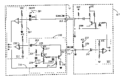
FIG.2 is a schematic of a bus driver circuit in
accordance with the present invention.
FIG.3 is schematic of an alternate bus driver circuit
in accordance with the present invention

5
-- ,~ r
~escription of a 'referred Embodiment
FIG. 1 is a radio frequency (RF) data communications
system having a fixed site transceiver 101 and a mobile
or portable transceiver 103. The mobile or portable
transceiver 103 sends and receives RF signals from the
fixed transceiver 101. The RF signals are coupled by ,the
antenna 105 and are demodulated and transformed into
data signals by the transceiver 107. The transceiver 107
can send or receive the data signals to peripherals on a
serial digital data bus 109. The peripherals in this
example are a handset 111 and a fax machine 113, but
other peripherals should not be excluded.
1 5 FIG. 2 reveals an exploded view of the digital data
bus between the transceiver 107 and the peripheral
handset 111. Although only the transceiver 107 and the
handset 111 are shown in FIG.2, the data bus can be used
in a multi-peripheral configuration. The digital data bus
2 0 109 is shown as uplink 211 and downlink 203. These
links allow for data transmission between the handset
111 and the trahsceiver 107. The data bus driver circuit
243 is common to all of the peripheral devices and
serves two main purposes. First, the data bus driver
25 circuit 243 is used to create a single voltage bias level
for the data bus uplink 211, eliminating -the varying
references points from each individual peripheral device
on th~ data bus by feeding the DC voltage level of the
data bus signal on the uplink 211 into the data bus drive
30 circuit 243. Second, it divides the voltage level of the
data signal output from the bus interface chip (RIG) 207
down to the amplitude of the data signals used on the
data bus 109. For the present invention, the amplitude of

6
-- .~ r~,
the voltage out of the chip is 5 Vpp and it is divided
dawn to an amplitude of 0.5 VpP, however, any other
comparable voltage divider scheme may be employed
here.
Since the data bus 109 uses small amplitude signals,
the data bus 109 must be driven around the same
reference point to insure proper priority control of the
data bus 109. The priority scheme for attaining control
of the data bus 109 is realized by the peripheral with the
lowest Q2 base voltage potential farting the base
emitter junction of C~2 on all of the other peripherals to
be reversed biased, therefore, preventing the other
peripherals from driving the bus. The common bias point
of all the peripherals is accomplished between with the
1 5 feedback through the transistor Q1 227 and C~2 213. The
circuit, including the resistor 231 and the capacitor 229
and the transistor C~1 227, removes the AC component of
the data signal on the bus 211. At the emitter of C~1 the
common bias voltage of the bus uplink 211 is present.
This common bias voltage level is then used to bias (~2.
As a result of this feedback operation, variances in
components or ground levels or power supply potentials
is eliminated with concern to this bus uplink 211 and
also variances in the voltage signal levels of the data
2 5 coming out of the bus interface chip 207.
The data signals output from the bus interface chip
207 on signal line 233 have an amplitude wi~ich varies
from one peripheral device to another, in this example,
the data signals output from the peripheral device has an
3 0 amplitude between 0 to 5 volts. The resister 217 and
the resistor 223 provide a voltage divider network which
reduces this amplitude down to a 0.5 Vpp about the bias
voltage present at the emitter of C~1 227. Resister 221

7
~ _,~,~~ ~J
and capacitor 219 form a filtering mechanism for
removing noise from the line. The inductor 215 also
contributes as a filtering mechanism.
Once the peripheral device obtains control of the bus
by pulling 233 to its lower state and holding it for a
specified amount of time, it turns on the transistor Q2
213 and the data is driven out the uplink 211 to the
transceiver 107. The voltage supply of the peripheral
225 can be different than the power supply of the
transceiver 237. Regardless of the differences, the data
bus will still have a common bias voltage. The original
bias level is generated by the transceiver power supply
237 and the resistor 239. The on/off switch 201, and
the downlink 203 is switched on when a peripheral is
first turned on. This grounds the downlink signifying to
the transceiver 107 that a new peripheral device 111 has
linked to the serial bus 109. The downlink is used to
send a common clocking source from the transceiver 107
to all the peripheral devices. All the data signals driven
out by a peripheral device 111 must have an effective
duty cycle of approximately 50%. An effective duty
cycle of 50% is' defined as an average value of the data
signal equal to 1/2 the voltage peak to peak. This allows
the bias point to stabilize at the middle of the transition
levels, allowing for proper recovery of the data by the
transceiver. !f the output signal line 233 remains in a
high or low state for a significant length of time, then
the DC bias level at the emitter of Q1 227. will
eventually adjust to the voltage level at which the data
is held, causing errors in the data transmission. This
potential problem is solved by sending manchester
encoded data which guarantees transitions in the data
signal.

s~~'''~,~~3 a
FIG. 3 is alternative embodiment to F1G. 2. The only
significant change in this embodiment is that the master
or the transceiver 107 determines the bias level at the
output of the emitter C~1 X15 to determine the bias level
by referencing the bias level off the downlink 303 which
comes from the master transc~iver 107. The rest of the
circuit contained here is identical to FIG. 2.
Thers are two essential parts of this embodiment.
First , the use of the DD voltage level of the data bus to
bias the data signal output from the peripheral devices.
This biasing eliminates the differences in
environmental characteristics, power supplies, ground
potential and signal levels of the individual peripheral
devices from the data signals. Second, adjusting the
amplitude of the signal output from the individual
peripheral device to a common low amplitude signal. By
adjusting this amplitude, there is a known voltage for
prioritising the bus access and lower EMI and RF!
emissions.

Representative Drawing
A single figure which represents the drawing illustrating the invention.
Administrative Status

2024-08-01:As part of the Next Generation Patents (NGP) transition, the Canadian Patents Database (CPD) now contains a more detailed Event History, which replicates the Event Log of our new back-office solution.

Please note that "Inactive:" events refers to events no longer in use in our new back-office solution.

For a clearer understanding of the status of the application/patent presented on this page, the site Disclaimer , as well as the definitions for Patent , Event History , Maintenance Fee  and Payment History  should be consulted.

Event History

Description Date
Inactive: IPC expired 2015-01-01
Inactive: IPC from MCD 2006-03-11
Time Limit for Reversal Expired 2005-02-21
Letter Sent 2004-02-20
Grant by Issuance 2001-05-08
Inactive: Cover page published 2001-05-07
Pre-grant 2001-02-07
Inactive: Final fee received 2001-02-07
Letter Sent 2000-12-01
Notice of Allowance is Issued 2000-12-01
Inactive: Approved for allowance (AFA) 2000-11-20
Amendment Received - Voluntary Amendment 2000-10-12
Inactive: Status info is complete as of Log entry date 2000-09-11
Inactive: Application prosecuted on TS as of Log entry date 2000-09-11
Inactive: S.30(2) Rules - Examiner requisition 2000-06-16
Application Published (Open to Public Inspection) 1992-09-17
Request for Examination Requirements Determined Compliant 1992-08-11
All Requirements for Examination Determined Compliant 1992-08-11

Abandonment History

There is no abandonment history.

Maintenance Fee

The last payment was received on 2001-01-05

Note : If the full payment has not been received on or before the date indicated, a further fee may be required which may be one of the following

  • the reinstatement fee;
  • the late payment fee; or
  • additional fee to reverse deemed expiry.

Please refer to the CIPO Patent Fees web page to see all current fee amounts.

Fee History

Fee Type Anniversary Year Due Date Paid Date
MF (application, 6th anniv.) - standard 06 1998-02-20 1997-12-31
MF (application, 7th anniv.) - standard 07 1999-02-22 1998-12-22
MF (application, 8th anniv.) - standard 08 2000-02-21 1999-12-14
MF (application, 9th anniv.) - standard 09 2001-02-20 2001-01-05
Final fee - standard 2001-02-07
MF (patent, 10th anniv.) - standard 2002-02-20 2002-01-07
MF (patent, 11th anniv.) - standard 2003-02-20 2003-01-06
Owners on Record

Note: Records showing the ownership history in alphabetical order.

Current Owners on Record
MOTOROLA, INC.
Past Owners on Record
BERNARD L. KNYCH
JAYESH M. PATEL
JEFFREY W. TRIPP
Past Owners that do not appear in the "Owners on Record" listing will appear in other documentation within the application.
Documents

To view selected files, please enter reCAPTCHA code :


To view images, click a link in the Document Description column. To download the documents, select one or more checkboxes in the first column and then click the "Download Selected in PDF format (Zip Archive)" or the "Download Selected as Single PDF" button.

List of published and non-published patent-specific documents on the CPD .

If you have any difficulty accessing content, you can call the Client Service Centre at 1-866-997-1936 or send them an e-mail at CIPO Client Service Centre.


Document
Description 
Date
(yyyy-mm-dd) 
Number of pages   Size of Image (KB) 
Cover Page 2001-04-23 1 53
Cover Page 1994-03-30 1 18
Abstract 1994-03-30 1 21
Claims 1994-03-30 7 125
Drawings 1994-03-30 3 76
Description 1994-03-30 8 276
Claims 2000-10-12 1 47
Representative drawing 1999-08-24 1 22
Representative drawing 2001-04-23 1 15
Commissioner's Notice - Application Found Allowable 2000-12-01 1 165
Maintenance Fee Notice 2004-04-19 1 173
PCT 1992-08-11 23 659
Correspondence 2001-02-07 1 23
Fees 1996-12-23 1 96
Fees 1996-01-09 1 95
Fees 1994-12-28 1 97
Fees 1993-12-24 1 97