Note: Descriptions are shown in the official language in which they were submitted.
q~ J9
IMPROVED SUPERCONDUCTIVE LAYER ON MONOCRYSTALLINE
SUBSTRATE AND PROCESS FOR ITS PREPARATION
The invention relates to superconductive
articles and processes for their preparation.
Agostinelli and others U.S. Patent-4,950,6~3
discloses the formation of superconductive thin films
formed by crystalline bismuth strontium calcium copper
oxide. The films are constructed by providing each
metal component of the final oxide in the form of a
metal-organic ligand compound, such as a metal
carboxylate; spin coating a solution of the metal-
ligand compounds in the desired stoichiometric ratio
onto a substrate; heating to decompose the organic
ligands; and then heating to a temperature in the range
of from 800 to 950C to crystallize the coating.
High transition temperature (>100K)
superconductive crystalline bismuth strontium calcium
oxide superconductive can be routinely prepared by the
process of Agostinelli and others. However, maximum
supportable critical current densities (the maximum
current density that permits superconductive current
transmission) have not been as high as those reportedly
achieved using other approaches for forming thin films.
There is a continuing need for articles
having more uniform crystal structure and increased
superconductive current carrying capacities.
This invention is directed to a
superconductive article comprised of a substrate having
a monocrystalline oxide surface provided by an oxide
chosen from the class consisting of (a) magnesium
oxide, (b) at least ~ne of zirconium oxide and hafnium
oxide, and (c) a perovskite and a superconductive
crystalline oxide layer epitaxially grown on the
substrate surface satisfying the formula:
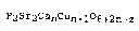
P2sr2cancun+lo6+2n-z
-
. .- .
29?
--2--
where
P represents Bi1_zPbz;
n is zero, 1 or 2; and
z is 0 to 0.30.
The superconductive crystalline oxide layer~ls
comprised of crystal unit cells each having two minor
axes and one major axis orthogonally related. The
superconductive article is characterized in that at
least 50 percent of the crystal unit cells are oriented
with their c-axes normal to the substrate surface and
with their minor axes relatively angularly aligned
within a deviation range of less than 5.
In another aspect this invention is directed
to a process of forming a superconductive article
comprised of a substrate having a monocrystalline oxide
surface provided by an oxide chosen from the class
consisting of (a) magnesium oxide, ~b) at least one of
zirconium oxide and hafnium oxide, and (c) a perovskite
and a superconductive crystalline oxide layer
epitaxially gro~n on the substrate surface satisfying
the formula:
P2Sr2CanCUn+l06~2n_ z
where
P represents Bil_zPbz;
n is zero, 1 or 2; and
z is 0 to 0.30.
The superconductive crystalline oxide layer being
comprised of crystal unit cells each having two minor
axes and one major axis orthogonally related, the
superconductive crystalline oxide layer being formed by
the steps of
(a) applying to the substrate a coating solution
comprised of a volatilizable film forming solvent and
metal-ligand compounds of each of P, Sr, Ca and Cu
, . . . -
~.
: ~ . ' : ~ . . :
containing at least one thermally volatilizable organic
ligand,
(b) removing the volatile components of the
coating by heating and
(c) forming the residual components of~the
coating into the superconductive crystalline oxide
layer by firing.
The process is characterized in that at least
50 percent of the crystal unit cells are oriented with
their c-axes normal to the substrate surface and with
their minor axes relatively angularly aligned within a
deviation range of less than 5 by (a') incorporating
at least one fluoro-substituted organic compound in the
coating solution to provide a F:Sr atomic ratio of at
least 3:1 and (c') firing to a temperature of from 800
to 860C in forming the superconductive crystalline
oxide.
The process of the invention offers the
advantages of producing superconductive articles of a
more uniform microstructure. The articles are capable
of supporting higher superconducting current densities
than have heretofore been realized using comparable
preparation procedures. Additionally, better quality
superconductive films are more readily realized at
lower firing temperatures as compared to conventional
processes that thermally decompose metal-organic ligand
compounds.
Figure 1 is an isometric schematic view of a
unit cell on a monocrystalline substrate surface;
Figures 2, 3 and 4 are isometric schematic
views of 2223, 2212 and 2~01 unit cell sub-units,
respectively;
Figure 5 is a plan detail of a conventional
superconductive oxide coating;
. , . , . , . .. . , ~ ~ . . - , . ~,
,: , .. . .. . . ~.
--4--
Figure 6 is a plan detail of a
superconductive oxide coating satisfying the
requirements of the invention;
Figures 7 and 8 are plots of X-ray
diffraction scattering angles versus the rel~tive
intensity of scatter; and
Figures 9(a) and 9(b) are photomicrographs of
thin films.
The present invention is directed toward
improving the crystal order and hence the
superconductive current carrying capacity of thin (< 5
~m) films containing crystalline oxides of bismuth
alkaline earth and copper. The invention is applicable
to a family of oxides that satisfy the general formula:
15 (~)
P2Sr2CanCUn+l06+2n_z
where
P represents Bil_zPbz;
n is zero, l or 2; and
z is 0 to 0.30.
Specifically preferred are the 2223 compositions of the
general formula:
(II)
P2 Sr2Ca2CU3010 - z
wherein P and z are as defined in formula I, and the
2212 compositions of the general formula:
(III)
P2 Sr2CalCU208 - z
wherein P is as defined in formula I and z is 0 to 0.2.
The oxides of formula I when properly
crystallized are capable of producing superconductive
thin films. A unit cell crystal structure compatible
with superconductivity is shown in Figure 1 oriented on
a monocrystalline substrate surface S8. The longest
--5--
dimension of the unit cell, its c-axis, is oriented
normal to the substrate surface parallel to arrow c.
The two remaining orthogonal (mutually perpendicular)
axes of the unit cell are parallel to the sub~trate
surface and parallel to the arrows a and b.~~Five unit
cell sub-units 1, 2, 3, 4 and 5 are shown on the
substrate surface, each sub-unit including (a) and (b)
portions relatively displaced along the c-axis (the
axis of longest length). Because of minor sub-unit to
sub-unit perturbations in the direction of the
b-axis(the axis of intermediate length~, approximately
5 sub-units along the b-axis are required to satisfy
the formal crystallographic definition requirements of
a unit cell. The unit cell a-axis (the axis of
shortest length) is one sub-unit in length. Notice
that the unit cell faces parallel to the c-axis (that
is, the vertical unit cell faces as shown in Figure 1)
are also each oriented parallel to one of the a and
b-axes.
The oxides of formula I can form any one of
three different superconductive crystal structures,
depending upon the value of n. When z is zero (that
is, when no lead is present) and ~ is 2, 1 or zero, the
structures schematically shown in Figures 2, 3 or 4,
respectively, result. In these figures the black
spheres represent copper, the unlabeled spheres
represent oxygen, and the spheres labeled ~, ~ and S
represent bismuth, calcium and strontium, respectively.
For ease of visualization an entire atom is shown in
each occurrence where any portion of the atom is
included in a sub-unit. ~Note that only a portion of
each atom lying at an edge or face of a sub-unit is
actually included within the sub-unit.) The central
tier of atoms of each (a) sub-unit form the four corner
tiers of each (b) sub-unit and vice versa.
~t~J~
--6--
In an actual monocrystalline film the sole difference
between an increment of layer thickness formed by (a)
sub-units and an increment of layer thickness formed by
(b~ sub-units is a relative shift of one half sub-unit
along each of the a and b axes. ~~
In a conventional superconductive thin film
satis~ying formula I the c-axes of the unit cells of
the crystalline oxide are oriented normal to the
substrate surface, as shown in Figure 1. The minor
axes (the a and b-axes) are parallel to the substrate
surface, with the a and b-axes of each unit cell being
orthogonally related. Over the entire surface of the
thin film there is, however, a wide array of different
angular orientations of minor axes.
The conventional angular deviation from
alignment of the minor axes of unit cells in a
conventional crystalline oxide thin film is shown in
Figure 5. The joined arrow pairs each indicate the
minor axes orientations viewed normal to the substrate
surface in that area of the film. While the arrows in
each joined pair exhibit a 90 angle of intersection,
significant angular displacements of minor axes
orientations are observed in different film areas.
The effect of the angular displacements of
minor axes orientations from one area of the film to
the next is to create a large number of individual
microcrystalline film segments (hereinafter referred to
as grains or microcrystals) separated by high angle
intergrain boundaries. ~ grain boundary (not shown in
Figure 5) separates each minor axes pair from each next
adjacent non-aliyned minor axes pair. Individual
microcrystalline grains on average typically have a
projected area viewed normal to the substrate surface
of less than about 100 ~m2. The areas of the
individual grains correlate inversely with the number
of high angle intergrain boundaries. Thus, the smaller
'`. :
' ' ,' ,, ` ~'
2~.P~
--7--
the mean projected areas of the grains, the greater the
number of high angle grain boundaries and the more
internal disruptions to superconduction within the thin
films. Thus, conventional thin films suffer the
disadvantage of exhibiting significantly limlted
superconductive current carrying capacity.
In the present invention a superconductive
crystalline oxide layer is epitaxially grown on a
monocrystalline substrate surface with a high degree of
matching not only of c-axis orientations, but also of
minor axes orientations. In every instance at least 50
percent (preferably greater than 70 percent and
optimally greater than 90 percent) of the unit cells
forming the superconductive layers are oriented with
their c-axes normal to the substrate surface and with
their minor axes relatively angularly aligned within a
deviation range of less than 5.
The feature of c-axis orientation normal to
the substrate surface can be realized for substantially
all of the unit cells in a thin film, with overall
deviations of less than 2 (often less than 1) from
normal of the c-axes being observed.
The distribution of the c-axes are determined
by rocking curve analysis. The orientation of the
crystal minor axes of the unit cells are determined by
the X-ray pole figure analysis technique. These
techniques are well understood by those skilled in the
art and are illustrated by B. D. Cullity, Elements of
X-ray Diffraction, 2nd Ed., Addison-Wesley, Reading,
Ma., Chapters 8 and 9, the disclosure of which is here
incorporated by reference. According to this technique
a point source of X-radiation is reflected from the
surface of the thin film with the thin film oriented
with a selected set of parallel crystallographic planes
within the thin film oriented parallel to the
reflection surface. The thin film is then rotated
.
- . . . , , ~ ,,
.: .. ... .
.
,
2~ 7~
--8--
about an axis normal to the selected crystal planes.
Reflection over a wide range of rotation angles
~referred to as azimuth angles) indicates a wide range
of unit cell axis orientations, while ideal alignment
is seen as four spot reflections separated on~ f~om ~he
other by a 90 rotation angle. In practice even in the
closest alignments produce spots that subtend at least
a small azimuth angle of rotation.
Applying the pole figure analysis technique
to a conventional film of the type shown in Figure 5
large azimuth angles of reflection are observed,
indicative of indicative of near random angular
displacement of minor axes from one grain to the next,
being observed.
Referring to Figure 6, a crystalline oxide
thin film satisfying the composition of formula I is
shown with minor axes pairs each representing minor
axes orientations in different areas of the film. As
in Figure 5, the c-axes are all normal to the
underlying (not shown) substrate surface, but, unlike
Figure 5, the minor axes pairs are largely in angular
alignment from one area of the film to the next. Using
X-ray pole figure analysis techniques near point (that
is, narrow azimuth angle) reflections are observed
subtending an azimuth angle of much less than 5, with
actual observations being of point deviations of less
than ~, typically in the order of 2. This is
indicative of a sharply diminished area to area angular
deviation of the minor axes pairs shown in Figure 6.
Since the unit cell axes of the crystalline
oxide films are orthogonal, once it is determined that
the minor axes are in angular alignment, marked
reduction in high angle intergrain boundaries in the
crystal structure are realized. Note that the
orthogonal configuration of unit cells makes it
immaterial whether a and b-axes in adjacent areas of
.. ..
~ J~
_g_
the film are relatively parallel or normally oriented,
so long as there is little angular displacement of the
minor axes pairs. Stated another way, referring to
Figures 5 and 6, essentially the same properties are
realized, regardless o~ which of the minor a~es in each
pair shown is labeled as an a-axis or a b-axi~.
By maximizing the angular alignment of the
minor axes pairs in planes parallel to the substrate
surface electrical current being conducted in the film
encounters a markedly reduced number of high angle
intergrain boundaries. This increases the current
carrying capacity of the thin films and produces
commensurate increases in the maximum currents that can
be transported under conditions of superconductivity.
The invention allows thin films, those of
less than 5 ~m thickness (most commonly less than 2 ~m
in thickness and optimally less than 1 ~m in thickness)
to be realized that exhibit both high superconductive
current densities and high temperatures of
superconductivity. Superconducting onset (To)
temperatures in excess of the temperature of liquid
nitrogen (77K) can be realized with the compositions
of formula I, and superconducting transition
tmeperatures (Tc) of greater than 100K are
contemplated. Maximum superconducting temperatures are
realized when n in formula I is 2, with progressively
lower temperatures being realizable when n is 1 or
zero. When n is zero both To and Tc are well below the
77K and 100K values noted above.
To achieve orientation of the crystalline
oxide thin film as described above it is necessary to
provide a monocrystalline substrate surface capable of
supporting epitaxial growth of the crystalline oxide.
In other words, the orientation of the thin film
crystalline oxide is derived from the crystalline order
of the monocrystalline substrate surface. Substrate
-10-
surfaces that exhibit a perovskite crystal structure
are particularly compatible witll supporting formation
of the oriented crystalline oxide thin film. Exemplary
of preferred perovskites for forming the subst~ate
surface are strontium titanate, lanthanum aluminate,
lanthanum gallium oxide and potassium tantalate. In
addition to the perovskites, monocrystalline magnesium
oxide (magnesia), hafnium oxide (hafnia) and zirconium
oxide (zirconia) are also useful materials for forming
the substrate surface supporting the oriented
crystalline oxide thin film. Hafnium and zirconium
have almost identical chemical and physical properties
and can be used interchangeably or mixed in any
proportions. As between hafnia and zirconia the latter
is less expensive and therefore much more extensively
employed in the art. Yttria stabilized zirconia, where
yttrium displaces from 5 to 15 percent of the zirconium
on an atomic basis, is a monocrystalline substrate that
has been widely used in fabricating superconductive
films. Although other crystal face orientations are
possible, the crystal surface presented by the
substrate for deposition of the oriented crystalline
oxide thin film is preferably a {100} surface.
The substrates can take any convenient form
capable of providiny the required monocrystalline
surface. The substrate can, for example, be a unitary
element formed throughout by a single monocrystalline
material. Alternatively, the substrate can contain a
monocrystalline support structure onto which one or
more layers are epitaxially grown to form the required
monocrystalline substrate surface. For example, on
monocrystalline silicon wafers monocrystalline layers
of monocrystalline layers of strontium titanate have
been epitaxially grown, as disclosed by H. Ishiwara and
K. Azuma, "Oriented Growth of SrTiO3 Films on Si(100)
Substrates Using In Situ Cleaning by Excited Hydrogen",
,
~ 2~'~$,~9
Mat. Res. soc. Symp. Proc., Vol. 116, 1988 Materials
- Research Society, pp. 369-375, and monocrystalline
layers of magnesia have been epitaxially grown, as
disclosed by D.K. Fork, F.A. Ponce, J.C. Tramontana and
T.H. Geballe, "Epitaxial MgO on Si(001) for-~-Ba-Cu-O
Thin-Film Growth by Pulsed Laser Deposition~, Appl.
Phys. Letter,58(20), 20 May 1991, pp. 2294-2296.
Monocrystalline layers of yttria stabilized zirconia
have been grown on sapphire (monocrystalline alumina),
as disclosed by H. Schmidt, K. Hradil, W. Hosler, W.
Wersing, G. Gieres and R.J. Seebock, ~Eipitaxial
YBa2Cu3Ox Thin Films on Sapphire Using a Y-Stabilized
Zr2 Buffer Layer~, Appl. Phys. Letter,59(2), 8 July
1991, pp. 222-224.
In addition to the materials named above
capable of providing a suitable monocrystalline
substrate surface it is recognized that still other
materials known to be capable of forming crystal
structures similar to that of the bismuth strontium
calcium copper oxides are known and can, if desired, be
employed to provide a suitable monocrystalline
substrate surface. Exemplary of less common materials
of this type are those of Takemura U.S. Patent
5,032,571, which discloses monocrystalline substrate
materials such as Bi2(Sr1_xLax)4Cu3O4 (x=0.05-0.4, y=8-
12); Bi4Ti312; CaBi4Ti4ols; SrBi4Ti4O15; Bagi4Ti4o15;
PbBi4Ti415; Sr2Bi4Ti518; Ba2Bi4TisOlg; and
Pb2Bi4Ti5ol8 -
Selecting a substrate capable of supporting
the epitaxial deposition of the crystalline oxide thin
film is essential, but insufficient in itself to
achieve the unit cell axial alignments described above.
Achieving alignment of minor axes has re~uired an
additional improvement in the procedure for depositing
the films. In addition to substrate selection the
present invention has been made possible by an
" ~ . .
,
.
-12-
improvement in the so-called "MOD" process of thin film
~ formation, described, ~or example, in Agostinelli and
others U.S. Patent 4,950,643, the disclosure of which
is here incorporated by reference.
In the MOD process the metals to be
incorporated in the film (that is, the metals of
formulae I, II or III) are each employed as starting
materials in the form of metal-ligand compounds, where
each metal-ligand compound includes at least one
thermally volatilizable organic ligand. The organic
ligands are selected for their film forming
capabilities. In general the film forming capabilities
of the organic ligands increase as a function of the
number of carbon atoms they contain and as a function
of chain branching, cyclic hydrocarbons and branched
hydrocarbon chains being capable of producing superior
films with fewer carbon atoms than linear hydrocarbon
chains. Typically organic ligands are selected that
contain up to about 30 carbon atoms. Individual metal
ligands can have as few as 2 carbon atoms (that is,
individual metal acetates are feasible), but preferably
contain from 6 to 20 carbon atoms. To improve the film
forming properties of the composition hydrocarbons or
substituted hydrocarbons, preferably branched chain
hydrocarbons or substituted hydrocarbons such as
terpenes, of from 10 to 30 carbon atoms can be
incorporated to assist in film formation.
In addition to selection on the basis of film
forming properties the metal-ligand compounds are
selected on their ability to thermally decompose rather
than vaporize. Metal-organic ligand compounds
(including metallo-organic and organo-metallic
compounds), such as metal alkyls, alkoxides, ~-diketone
derivatives and metal salts of organic acids--for
example, carboxylic a~ids, constitute preferred metal-
ligand compounds. Copper is preferably employed as a
,
-
-13-
metal carboxylate to minimize copper loss by
vaporization.
Exemplary preferred organic ligands for the
metal organic compounds include metal butyrates, 2-
ethylhexanoates, naphthenates, neodecanoates,butoxides, isopropoxides, rosinates ~for example,
abietates), cyclohexanebutyrates and acetylacetonates.
Exemplary film-forming agents include 2-ethylhexanoic
acid, rosin (for example, abietic acid), ethyl lactate,
2-ethyoxyethyl acetate and pinene.
Any convenient thermally decomposable or
volatilizable solvent for the metal-ligand compounds
and the film-forming agents can be employed. Exemplary
preferred film forming solvents include toluene, 2-
ethylhexanoic acid, n-butyl acetate, ethyl lactate,
propanol, pinene and mineral spirits.
It has been discovered ~uite unexpectedl~
that the incorporation of fluoro-substituted organic
compounds (herein employed to mean compounds containing
one or more fluorine to carbon bonds) in the metal-
organic coatings allows the unit cell axial alignmellts
described above to he obtained. The result is even
more surprising, since no evidence has been found that
the fluorine remains in the crystalline oxide thin film
after it emerges from ~iring.
It has been established that the
effectiveness of fluoro-substituted organic compounds
to achieve unit cell axial alignment results from
having present in metal-ligand coating a critical ratio
of strontium to fluorine atoms. With a F:Sr atomic
ratio of 2:1 unit cell axial alignment is not attained.
At least a 3:1 F:Sr atomic ratio is required for unit
cell axial alignment, with at least a 4:1 F:Sr atomic
ratio being preferred. While in general no further
advantage can be realized by increasing the F:Sr atomic
ratio above 8:1, it is possible to increase the F:Sr
. ~ .
:
: - . . . - ~
, ~ .. .. . .
-14-
atomic ratio to 100:1 or more without adverse effect.
F:Sr atomic ratios of from 4:1 to 50:1 are generally
preferred, with atomic ratios of from 8:1 to 20:1 being
optimum.
The requisite fluorine content can-be
incorporated in the metal-organic ligand coatings by
introducing any convenient organic compound having one
or more fluorine to carbon bonds. While fluoro-
substituted or~anic compou~ds can be selected solely
for their utility in supplying the required fluorine
atoms, it is preferred to select fluoro-substituted
organic compounds satisfying the film forming
characteristics discussed above to insure intimate
dispersion of the fluorine atoms in the coatings. In a
specifically preferred form of the invention the
ligands of the metal-organic compounds and/or the film-
forming agents are fluoro-substituted, thereby
obviating the necessity of including yet another
ingredient in forming the coating. It is spe~ifically
contemplated to blend a metal-organic compound lacking
fluorine substitution with a similar fluoro-substituted
metal organic compound to achieve the exact proportion
of fluorine to strontium desixed. The highest levels
of precision in establishing fluorine to strontium
ratios is realized by including fluoro-sub~tituents in
the strontium-organic ligand compound. This
establishes the F:Sr ratio independently of any
variances in blending other components.
Once a coating composition has been
formulated containing the metals of formulae I, II or
III in their indicated ratios and the desired F:Sr
ratio, the coating composition is applied to the
monocrystalline support surface by any convenient
coating technique. Spin casting is a particularly
preferred technique, since it allows control of both
the thickness and uniformity of the spin cast layer.
.
~ ?7~
-15-
Spin casting is well suited for laying down layers of
up to about 1.5 ~m in thickness, but spin cast layers
are typically less than 1.0 ~m in thickness.
Following coating of the metal-organic
compounds the coated substrate is heated to a
temperature sufficient to volatilize or decompose
thermally the organic components of the coating. ~ile
removal temperatures vary as a function of the organic
components selected, no organic residue remains at a
temperature of 600C. Although this temperature is
well in excess of that required to remove organic
residues from the coating, it is still well below the
temperatures required for crystalline oxide formation.
Because of solvent removal as well a~ thermal
decomposition of organic ligands the coating after
heating is much thinner than that originally coated.
If a thicker crystalline oxide coating is desired than
can be generated using a single spin casting step, it
is recognized that the spin casting step and the
heating step can be repeated, once or several times, in
sequence to achieve the desired crystalline oxide film
thickness. Successive coating and heating steps also
offer the advantage of better protecting the coating
from substrate contaminants, if present.
Conversion of the coating after removal of
organic residues to a crystalline oxide with unit cell
a~ial alignment can be achieved at temperatures in the
range of from 800 to 860C. Crystallization
temperatures are a function of both the lead content of
the coating and the crystalline form being formed. The
2101, 2212 and 2223 crystalline forms require
progressively high temperatures for their formation.
For the 210~ crystalline form preferred firing
temperatures are in the range of from 800 to ~0C.
For the 2212 crystalline form preferred firi~g
temperatures are in the range of from 800 to 850C,
7~
-16-
which is below the 850 to 920C preferred range for the
2212 crystalline form taught by Agostinelli and others.
For the 2223 crystalline form preferred firing
temperatures are in the range of from ~00 to 860C,
which is well below the approximately 890C-~iring
temperature typically employed to produce this
crystalline form.
If desired, the steps of coating, heating and
firing described above can be repeated in se~uence two
or more times to produce a thin film having increased
mean grain projected areas.
Apart from the features specifically
discussed, above fabrication of the crystalline oxides
with unit cell aligned crystal axes can take any
convenient conventional form. The thin films can, for
example, be formed as taught by A~ostinelli, cited
above, except as otherwise noted.
Exam~les
Except as otherwise indicated all weight
percentages are based on total weight.
Example 1 (Control)
A metal-organic ligand composition containing
bismuth, strontium, calcium and copper in a 2:2:1:2
atomic ratio (hereinafter referred to as 2212 Precursor
1) was prepared by mixing a bismuth precursor
composition containing bismuth 2-ethylhexanoate, a
strontium precursor composition containing strontium
cyclohexanebutyrate, a calcium precursor composition
containing calcium 2-ethylhexanoate and a copper
precursor composition containing copper 2-
ethylhexanoate. The bismuth precursor, containing
18.73% by weight bismuth, and the calcium precursor,
containing 4.10% by weight calcium, were prepared as
described by Agostinelli and others U.S. Patent
,
,
2~?17~ ,
-17-
4,950,643. The strontium precursor was strontium
cyclohexane-butyrate purchased commercially with an
assay indicating a strontium concentration of 19~4~ by
weight strontium. The copper precursor, with a cop~er
concentration o~ 6.31% by weight, was prepared by
mixing 2.0 g of copper acetate with 8.0 g of 2 ethyl-
hexanoic acid. The individual precursors were mixed in
a weight ratio of 1:0.438:0.405:0.903 and then heated
to boiling until no solids remained. The 2212
Precursor 1 had a concentration of about 1.63 X 10⁻⁴
mole (based on the 2212 crystalline oxide to be formed)
per gram. To enhance its film forming properties 7% by
weight of Kodak 2315TM(rosin) was added with gentle
heating until all the rosin was dissolved.
2212 Precursor 1 was spin coated on a {100}
crystal surface of magnesium oxide at 4000 rpm for 20
seconds. The coated film was then heated on a hot
plate to a thermal decomposition temperature of 450C.
The coating then fired in air at a temperature of 865C
for 10 minutes in air.
Microscopic examination revealed a
polycrystalline coating on the substrate surface having
a mean grain effective circular diameter (ECD) in the
range of from 1 to 2 ~m. X-ray diffraction analysis of
c-axis alignment revealed a large number of c-axis
misaligned grains.
The superconducting onset temperature To was
determined to be 76K. The critical current density
increased slowly with decreasing temperature, reaching
a value of approximately 1 X 10⁴ A/cm2 at 40K. The
magnetic susceptibility measured versus temperature
exhibited a strong field dependence, corroborating poor
intergranular conductivity and low critical current.
This control demonstrates low critical
currents produced by a conventional procedure of
preparing a superconductive 22~2 bismuth strontium
...
4 ;i~
-18-
calcium copper oxide crystalline oxide coating with a
high level of c-axis misalignment on a monocrystalline
magnesia substrate surface.
Example 2 ~Control) --
This example repeated the steps of Example 1,
except that the final film was built up using four
repetitions of the coating, heating and firing steps,
with each repetition producing a layer having a
thickness of 60 nm, measured after hot plate heating.
The four-layer coating had an overall thickness of 250
nm.
Rocking curve analysis revealed a high degree
of c-axis orientation normal to the substrate surface,
with 5Q percent of the microcrystals having c-axis
orientations deviating from the perpendicular by less
than 0.3 to 0.4. X-ray diffraction analysis of minor
axis orientations revealed a high degree of angular
misalignment. This is demonstrated in Figure 7 by the
three diffraction peaks covering a range of about 40
with an angle of 12 to 13~ separating adjacent peaks.
The superconducting onset temperature was
80C, and the critical current remained low with
magnetic susceptibility still showing a strong field
dependence.
This control demonstrates that c-axis
alignment with angular misalignment of the minor axes
is insufficient to improve the superconductive current
carrying capacity of a coating.
Example 3
The procedure of Example 1 was repeated,
except that (a) the 2212 Precursor 1 was mixed with
heptafluorobutyric acid at a ratio of 1:0.17 (F:Sr
atomic ratio 8:1) and firing was conducted for 30
-- :
,
%~7~
-19-
minutes at 820C. Some grains were 30 to 50 ~m wide
- and several hundred ~m long.
Rocking curve analysis of the Bi2Sr2CaCu2Og~
film revealed a high degree of c-axis orientation
normal to the substrate surface, similar to~~hat of
Example 2. However, unlike Example 2, the thin film
also demonstrated a high degree of angular alignment of
the minor axes. This is demonstrated in Figure 8 by
the single diffraction peak extending over an angle of
only 2C.
The superconducting onset temperature To was
determined to be 81K. The critical current density
increased slowly with decreasing temperature, reaching
a value of approximately 9 X 10⁴ A/cm2 at 40K. The
magnetic susceptibility measured versus temperature
exhibited a much weaker field dependence than in
Example 1.
This example demonstrates that both c-axis
alignment and angular alignment of the minor axes can
be realized by introducing fluoro-substituted organic
compounds during initial coating. The enhanced unit
cell orientation produced a 9 times increase in
critical current as compared to control Example 1. It
is also significant that the incorporation of fluoro-
substituted organic compound in the coating allowed thefiring temperature to be reduced by 45C.
Example 4 (Control)
Example 1 was repeated, except that coating
was undertaken onto the {100} monocrystalline surface
of a strontium titanate perovskite.
The thin film produced was essentially
similar to that of Example 1 in its crystal structure
and conduction properties.
A microscope view of the thin film is shown
in Figure 9(a).
:-" 2~ "~7~
-20-
Example 5
The procedure of Example 4 was repeated,
except that (a) the 2212 Precursor 1 was mixed with
heptafluorobutyric acid at a ratio of 1:0.17 (F:Sr
atomic ratio 8:1) and firing was conducted for 30
minutes at 820C.
X-ray diffraction, optical microscopy and
Raman spectrometry measurements revealed c-axis normal
alignment on the substrate surface with the minor axes
also being angularly aligned. The alignment of the
microcrystals on the surface of the substrate is shown
in Figure 9(b). X-ray pole figure examination showed a
narrow spot pattern, corroborative of angular alignment
of the minor axes of the crystal unit cells.
Volume susceptibility measurements showed the
field dependence was 10 times less than that of the
thin film of Example 4, suggesting an order of
magnitude increase in the superconductive current
carrying of the thin film of this example as compared
to that of Example 4.
This example demonstrates the effectiveness
of a fluoro-substituted organic compound when
incorporated in the initial coating to increase axial
alignment of the crystalline oxide and hence the
superconductive current carrying capacity of the thin
films. This example further demonstrates the utility
of a substrate surface exhibiting a perovskite crystal
structure in realizing the advantages of the invention.
Example 6
Example 5 was repeated, except that the F:Sr
atomic ratio in the coating was reduced to 4:1 by
decreasing the amount of heptafluorobutyric acid
introduced into the initial coating composition.
The thin film crystal and conduction
properties were similar to those of Example 5.
. .. .: :.. : - . . .. ... . . .. . . .
-21-
Example 7 (Control)
Example 5 was repeated, except that the F:Sr
atomic ratio in the coating was reduced to 2:1 by
decreasing the amount of heptafluorobutyric acid
introduced into the initial coating compositlon.
The thin film produced was granular in
appearance, similar to the thin film of Example 1, but
with the mean ECD of the grains increased to 5 to 6 ~m.
This example demonstrates that a 2:1 atomic
ratio of F:Sr provides insufficient fluoro substitution
of the organic compounds to realize more than marginal
advantages of the invention.
,.
.. . . ....: .
: ~: ;,~ .