Note: Descriptions are shown in the official language in which they were submitted.
2076323
1 TITLE OF THE INVENTION
CALL SIGNAL GENERATING CIRCUIT
BACKGROUND OF THE INVENTION
The present invention generally relates to
call signal generating circuits, and more particularly
to a call signal generating circuit which generates a
call signal by carrying out a switching control.
A call signal which is used to call and ring
the bell of the telephone set from the switching system
is also sometimes referred to as a ringing signal. For
example, a low-frequency signal of 16 Hz and 75 V is
turned ON for one second and turned OFF for two seconds
to form the call signal. The call signal is generated
by a call signal generating circuit, and there is a
demand to improve the characteristic and efficiency of
the call signal generating circuit. The call signal was
originally a sinusoidal wave, but the call signal was
replaced by a staircase wave which approximates the
crest factor of the sinusoidal wave.
Generally, the voltage supplied from the
switching system to the telephone set of the subscriber
is 48 V. On the other hand, the call signal has the
frequency of 16 Hz and the peak voltage of 75 V. Hence,
a step-up transformer is used to boost the voltage when
forming the call signal. However, the step-up
transformer designed for the low-frequency of
approximately 16 Hz is bulky, and the method of boosting
the voltage using a high-frequency signal was
conventionally used.
FIG.1 shows an example of a conventional call
signal generating circuit. The conventional call signal
generating circuit includes a transformer 41 having a
primary winding 41a and secondary windings 41b and 41c,
a transistor 42, a capacitor 43, diodes 44 and 45,
photo-transistors 46 and 47, a capacitor 48, a control
circuit 49, photodiodes 50 and 51, a dummy resistor 52
~L
- ` 2076~3
_ - 2
1 and output terminals 53 which are connected as shown in
FIG.1.
A D.C. voltage is applied to the primary
winding 41a of the transformer 41 via the transistor 42,
and this transistor 42 is turned ON/OFF at a frequency
of several tens of kHz to several hundred kHz by the
control circuit 49. Accordingly, compared to the case
where the 16 Hz signal is boosted, it is possible to
reduce the size of the transformer 41. The voltage of
several tens of kHz to several hundred kHz induced at
the secondary windings 41b and 41c of the transformer 41
due to the ON/OFF control of the transistor 42 is
rectified by the diodes 44 and 45. The diode 44
rectifies the voltage into a positive polarity voltage,
while the diode 45 rectifies the voltage into a negative
polarity voltage. The phototransistors 46 and 47 are
respectively turned ON/OFF by the voltages from the
diodes 44 and 45t and the phototransistors 46 and 47 are
turned ON/OFF alternately. Hence, a positive polarity
voltage from the phototransistor 46 and a negative
polarity voltage from the phototransistor 47 are output
alternately, and a call signal of 16 Hz is output via
the output terminals 53.
In this case, a photo coupler is formed by the
phototransistor 46 and the photodiode 50, and another
photo coupler is formed by the phototransistor 47 and
the photodiode 51. The photodiodes 50 and 51 are
alternately driven by the control circuit 49 for a time
which is shorter than one-half the period of the 16 Hz
call signal. Accordingly, the phototransistors 46 and
47 are alternately turned ON with respective quiescent
times. The capacitor 48 is provided to eliminate
switching frequency components of several tens of kHz to
several hundred kHz induced at the secondary windings
41b and 41c, other high-frequency components and the
like. The dummy resistor 52 is provided to discharge
the capacitor 48.
2076323
1 FIG.2 is a time chart for explaining the
operation of the conventional call signal generating
circuit shown in FIG.l. In FIG.2, (a) shows a current
supplied to the photodiode 50l (b) shows a current
supplied to the photodiode 51, and (c) and (d) show the
call signal output via the output terminals 53. As
described above, the photodiodes 50 and 51 receive the
currents from the control circuit 49. If the 16 Hz call
signal has a period T1, the current is supplied to the
photodiode 50 for a time T2, the current is supplied to
the photodiode 51 for a time T4 and quiescent times T3
and T5 are provided as shown in FIG. 2, measures are
taken so that Tl = T2+T3+T4+T5, T2 = T4 and T3 = T5. In
this case, the crest factor of the sinusoidal signal
which is equal to (crest value)/(effective value) is
1.414, and the quiescent times T3 and T5 are set so as
to approximate this crest factor. The effective value
is the average of the square of the instantaneous value
of one period of the fundamental wave, and the crest
value is the peak value of the wave.
When the currents are supplied to the
photodiodes 50 and 51 which form the photo coupler with
the respective phototransistors 4 6 and 47, the photo-
transistors 46 and 47 are turned ON by the light from
the photodiodes 50 and 51 applied to the bases of the
phototransistors 46 and 47. The phototransistors 46 and
47 are respectively turned ON during the times T2 and T4
in FIG. 2. As a result, it is possible to obtain the
call signal which has the staircase waveform with the
crest factor approximating the crest factor of the
sinusoidal wave.
If the dummy resistor 52 is omitted and the
call signal generating circuit assumes a low-load state,
it becomes equivalent to the case where the discharge
time constant of the capacitor 48 is large. Hence, the
falling edge (and the corresponding rising edge) of the
waveform becomes gradual in this case as shown in FIG.2
2076323
-- 4
1 (d). That is, the waveform shown in FIG.2 (d) is
different from the waveform which is set to have the
crest factor approximating the crest factor of the
sinusoidal wave and does not meet the specifications.
Therefore, the dummy resistor S2 is essential in the
conventional call signal generating circuit.
As described above, the 16 Hz call signal is
generally used. However, in order to reduce the size of
the step-up transformer, the method of boosting the
voltage by a high-frequency switching is conventionally
used. In this case, the call signal used has the
staircase waveform shown in FIG.2 (c) which has the
crest factor approximating the crest factor of the
sinusoidal wave. The dummy resistor 52 is provided to
maintain this staircase waveform shown in FIG.2 (c).
However, there were problems in that a power loss is
introduced at the dummy resistor 52 and that the heat
generated from the dummy resistor 52 prevented the
effective reduction of the size of the call signal
generating circuit.
In other words, the power loss at the dummy
resistor 52 is large if the resistance of the dummy
resistor 52 is small. However, the discharge of the
capacitor 48 becomes insufficient if the resistance of
the dummy resistor 52 is made large in order to reduce
the power loss. For this reason, it was inevitable to
set the resistance of the dummy resistor 52 to the small
value in order to ensure sufficient discharge of the
capacitor 48, although the unwanted power loss occurred.
SUMMARY OF THE INVENTION
Accordingly, it is a general object of the
present invention to provide a novel and useful call
signal generating circuit in which the problems
described above are eliminated.
Another and more specific object of the
present invention is to provide a call signal generating
207632~
- 5
1 circuit comprising a step-up transformer having a
primary winding and secondary windings, first switching
means, coupled between the primary winding of the
step-up transformer and a D.C. power source, for turning
ON/OFF at a frequency higher than a frequency of a call
signal which is to be generated by the call signal
generating circuit, rectifying means, coupled to the
secondary windings of the step-up transformer, for
rectifying voltages induced at the secondary windings
into a positive polarity voltage and a negative polarity
voltage, second switching means, coupled to the
rectifying means, for alternatively outputting the
positive polarity voltage and the negative polarity
voltage with a quiescent time in which both the positive
and negative polarity voltages are not output, a
capacitor, having first and second terminals coupled to
the second switching means, for receiving the positive
and negative polarity voltages output from the second
switching means, a resistor coupled to the first
terminal of the capacitor, third switching means,
coupled to the resistor, for discharging the capacitor
during the quiescent time, the resistor and the third
switching means being coupled in series to form a series
circuit which is coupled in parallel to the first and
second terminals of the capacitor, and a pair of output
terminals, respectively coupled to the first and second
terminals of the capacitor, for outputting the call
signal. According to the call signal generating circuit
of the present invention, the power loss introduced at
the resistor is reduced to a negligible extent because
the third switching means is turned ON/OFF, and the heat
generated by the resistor is accordingly reduced.
Therefore, the size of the call signal generating
circuit can be reduced compared to the conventional call
signal generating circuit. In addition, the falling
edge (and the corresponding rising edge) of the call
signal can be made sharp by the provision of the third
2076323
-- 6 --
1 switching means.
Other objects and further objects of the
present invention will be apparent from the following
detailed description when read in conjunction with the
accompanying drawings.
BRIEF DESCRIPTION OF THE DRAWINGS
FIG.1 is a circuit diagram showing an example
of a conventional call signal generating circuit,
FIG.2 is a time chart for explaining the
operation of the conventional call signal generating
circuit shown in FIG.l;
FIG.3 is a circuit diagram for explaining the
operating principle of a call signal generating circuit
according to the present invention;
FIG.4 is a circuit diagram showing an
embodiment of the call signal generating circuit
according to the present invention;
FIG.5 is a time chart for explaining the
embodiment shown in FIG.4; and
FIGS.6 and 7 are time charts for explaining
the effects of the present invention in comparison with
the conventional call signal generating circuit.
DESCRIPTION OF THE PREFERRED EMBODIMENTS
First, a description will be given of the
operating principle of a call signal generating circuit
according to the present invention, by referring to
FIG.3.
The call signal generating circuit shown in
FIG.3 includes a transformer 1, a transistor 2, a
rectifying circuit 3, transistors 4 and 5, a capacitor
6, a resistor 7, a switching circuit 8, a control
circuit 9, and output terminals 10 which are connected
as shown.
The transistor 2 is connected between the
primary winding of the transformer 1 and the D.C. power
2076323
-- 7
1 source (not shown), and this transistor 2 is turned
ON/OFF at a frequency which is high compared to the
frequency of the call signal which is generated by the
call signal generating circuit. The rectifying circuit
3 rectifies the voltages induced at the secondary
windings of the transformer 1 into positive and negative
polarity voltages.
The transistors 4 and 5 are alternately turned
ON/OFF depending on the period of the call signal so as
to respectively output the positive and negative
polarity voltages from the rectifying circuit 3. The
transistors 4 and 5 are controlled so that there exist
quiescent times in which both the transistors 4 and 5
are turned OFF simultaneously. The positive and
negative polarity voltages from the transistors 4 and 5
are applied to the capacitor 6.
The switching circuit 8 is turned ON during
the quiescent time in which both the transistors 4 and 5
are OFF simultaneously. When the switching circuit 8 is
ON, the charge in the capacitor 6 is discharged via the
resistor 7. The control circuit 9 controls the
transistors 2, 4 and 5, and the switching circuit 8.
The call signal is output via the output terminal 10.
As described above, the voltages are induced
at the secondary windings of the transformer 1 by
turning the transistor 2 at a frequency higher than the
frequency of the call signal. The voltages induced at
the secondary windings of the transformer 1 are
rectified into the positive and negative polarity
voltages by the rectifying circuit 3, and the positive
polarity voltage is output via the transistor 4 while
the negative polarity voltage is output via the
transistor 5. Accordingly, by alternately turning the
transistors 4 and 5 ON/OFF, it is possible to output a
16 Hz call signal from the output terminals 10.
By providing the quiescent time in which both
the transistors 4 and 5 are turned OFF simultaneously,
2076323
-- 8
1 it is possible to obtain a call signal which has the
staircase waveform. The charge in the capacitor 6 is
discharged via the resistor 7 by turning the switching
circuit 8 ON during the quiescént time. In other words,
even under the low-load state, it is possible to make
the falling edge (and the corresponding rising edge) of
the staircase wave sharp. In addition, because the
switching circuit 8 is turned OFF during the time in
which the positive or negative polarity voltage is
output via the transistors 4 or 5, no power loss is
introduced due to the resistor 7 during this time.
Next, a description will be given of an
embodiment of the call signal generating circuit
according to the present invention, by referring to
FIG.4.
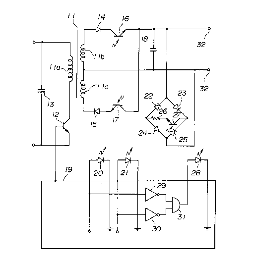
The call signal generating circuit shown in
FIG.4 includes a transformer 11 having a primary winding
lla and secondary windings llb and llc, a transistor 12
connected to the primary winding lla of the transformer
11, a capacitor 13, diodes 14 and 15, phototransistors
16 and 17, a capacitor 18, a control circuit 19,
photodiodes 20 and 21, diodes 22 through 25, a resistor
26, a phototransistor 27, a photodiode 28, and output
terminals 32 which are connected as shown. The control
circuit 19 includes inverters 29 and 30, and an AND
circuit 31 which are connected as shown.
The diodes 22 through 25, the phototransistor
27 and the photodiode 28 form a switching circuit which
corresponds to the switching circuit 8 shown in FIG.3.
By connecting the diodes 22 through 25 to form a bridge
connection, it is possible to use a unipolarity
switching element such as the phototransistor 27. A
photo coupler is formed by the phototransistor 16 and
the photodiode 20, and another photo coupler is formed
by the phototransistor 17 and the photodiode 21. A
photo coupler is also formed by the phototransistor 27
and the photodiode 28. It is of course possible to use
- ` 2076323
a normal transistor in place of each of these photo
couplers.
The control circuit 19 controls the transistor
12 so that the transistor 12 turns ON/OFF at a frequency
on the order of several tens of kHz. In addition, the
control circuit 19 alternately supplies a current to the
photodiodes 20 and 21 with the quiescent time. This
control circuit 19 includes the inverters 29 and 30, and
the AND circuit 31. The control circuit 19 may be
realized by logic circuits or a programs of a
microprocessor, similarly as in the case of the
conventional call signal generating circuit.
The transistor 12 which is connected to the
primary winding lla of the transformer 11 is turned
ON/OFF by the control circuit 19 at the frequency of
several tens of kHz, and the voltages induced at the
secondary windings llb and llc of the transformer 11 are
respectively rectified into the positive and negative
polarity voltages by the diodes 14 and 15. The positive
and negative polarity voltages are respectively applied
to the phototransistors 16 and 17. In addition, because
the current is alternately supplied to the photodiodes
20 and 21 with the quiescent time to emit light from the
photodiodes 20 and 21, the phototransistors 16 and 17
turn ON/OFF responsive to the light from the
. corresponding photodiodes 20 and 21. As a result, the
positive and negative polarity voltages are alternately
output from the output terminals 32 with the quiescent
time.
During the time in which the current is
supplied to the photodiodes 20 and 21, the output of the
AND circuit 31 is "0", and thus, the photodiode 28 does
not emit light. Accordingly, the phototransistor 27 is
OFF during this time, and no current flows to the
resistor 26 during the time in which the positive or
negative polarity voltage is output. Furthermore,
during the quiescent time in which no current is
~076323
-- 10 --
1 supplied to the photodiodes 20 and 21, the output of the
AND circuit 31 is "1", and thus, the photodiode 28 emits
light in response to the current which is received.
Therefore, the phototransistor 27 is turned ON
responsive to the light emitted from the photodiode 28,
and the charge of the capacitor 18 is discharged by the
resistor 26 during the quiescent time of the
phototransistors 16 and 17 via the bridge-connected
diodes 22 through 25 and the phototransistor 27. In
other words, even in the low-load state, it is possible
to make the falling edge (and the corresponding rising
edge) of the call signal waveform sharp.
FIG. 5 is a time chart for explaining the
operation of the embodiment shown in FIG. 4. In FIG. 5,
(a) shows the current supplied to the photodiode 20, (b)
shows the current supplied to the photodiode 21, (c)
shows the current supplied to the photodiode 28, and (d)
shows the call signal output from the output terminals
32. If one period of the 16 Hz call signal is denoted
by T1, the relationship T1 = T2+T3+T4+T5, T2 = T4 and T3
= T5 stand, similarly as in the case of the conventional
call signal generating circuit. The phototransistor 27
turns ON during the quiescent times T3 and T5 so as to
discharge the charge of the capacitor 18. Hence, the
call signal shown in FIG. 5 (d) having the sharp falling
edge (and corresponding rising edge) is output from the
output terminals 21.
The circuit construction of the switching
circuit 8 is not limited to that of the embodiment shown
in FIG.4. For example, it is possible to form the
switching circuit 8 by analog switching elements,
instead of forming the neutral switching circuit from
the phototransistors 27 and the bridge-connected diodes
22 through 25. Moreover, it is possible to provide two
single polarity switching elements such as the
phototransistor 27 and to discharge the charge of the
capacitor 18 by turning ON the single polarity switching
2076323
-- 11 --
1 elements depending on the sequence with which the
current is supplied to the photodiodes 20 and 21, that
is, depending on the charge polarity of the capacitor 18.
FIGS.6 and 7 are time charts for explaining
the effects of the present invention in comparison with
the conventional call signal generating circuit.
FIG.6 shows the call signal waveform obtained
by the conventional call signal generating circuit shown
in FIG.l. In FIG.6, (a) shows the call signal waveform
when no telephone set is connected to the call signal
generating circuit, and (b) shows the call signal
waveform when one telephone set is connected to the call
signal generating circuit. As may be seen from FIG.6,
particularly the falling edge (and the corresponding
rising edge) of the call signal waveform is gradual.
On the other hand, FIG.7 shows the call signal
waveform obtained by the call signal generating circuit
shown in FIG.4. In FIG.7, (a) shows the call signal
waveform when no telephone set is connected to the call
signal generating circuit, and (b) shows the call signal
waveform when one telephone set is connected to the call
signal generating circuit. As may be seen from FIG.7,
the falling edge (and the corresponding rising edge) of
the call signal waveform is sharp compared to the call
signal waveform shown in FIG.6.
Further, the present invention is not limited
to these embodiments, but various variations and
modifications may be made without departing from the
scope of the present invention.