Note: Descriptions are shown in the official language in which they were submitted.
2076~0~
SZ 9-91-011
DESCR IPTION
Improved AiGalnP Diodes Emitting Visible Light
TECHNICAL FIELD
-
In some optoelectronic applications there is a special need for visible laser
diodes lasing with a wavelength between 600 nm and 700 nm, and visible light
emitting diodes (LEDs). The performance and reliability of these devices have tomeet special requirements as there are e.g. high output power, continuous wave
operation, low thermal and electrical resistance. Laser diodes consisting of
AlGalnP/GalnP allow to fabricate lasers emitting lightwaves having wavelength
lower than 700 nm. Different AlGalnP/GalnP device structures have been
reported qualifying these types of lasers and LEDs to be the most promising onesfor several Future optoelectronic applications.
BACKGROUND OF THE INVENTION
AlGalnP/GalnP visible lasers and light emitting diodes are light sources which
could be utilized for various optoelectronic applications including high-densityoptical disks, laser printers, plastlc fiber communication, bar-code readers~
pumping of solid state lasers, laser surgery, and optical measurement systems
which presently use He-Ne lasers.
The following sections relate mainly to optical storage systems employing laser
diodes. The requirements of these laser diodes meet the requirements of laser
diodes used in the other appllcations mentioned above. The semiconductor laser
diode used for storing data on high-density optical disks is a key componen-t
because the wavelength of the radiation determines to a large extent the
achievable storage density. Other requirements For these lasers are higher
available optical power, which is limited by COD (Catastrophic Optical l:~amage)of the device, and improved re!iabillty which is crucial for the overall system
.~
~ .
2076~o~
2 SZ 9-91-017
reliability. Known storage systems are based on AlGaAs lasers, laslng at a
wavelength of 780 nm and reaching power levels of ~; 30 mW. Laser dlodes with
reduced wavelength, 7mproved optical output power and lifetime are important
for future stsrage systerr~s and the other optoelectronlc applicatlons mentioned,
Different technical proposals are known to improve optical storage systems One
important development are devices emitting short wavelength which are based
on second harmonic generation in non-linear optical material The output power
and reliability of these devices is not satisfying. The employment of improved
AlGalnP/GalnP iaser diodes with a wavelength of about 670 nm, increased output
power and performance would allow for a 30 percent increase in storage density
and an improved reliability of the whole storage system.
The quaternary AlGalnP, lattice matched to GaAs, having a direct bandgap up to
2.3 eV, is presently the most interesting candidate for the above mentioned
applications. Owing to advanced growth techniques, it has become possible to
utilize the quaternary AlGalnP for diodes emitting in the range between 600 and
700 nm. One advantage of AlGalnP is the complete lattice match to crystalline
quality binary ~3aAs substrate. In fact, almost all AiGalnP diodes reported today
have been grown by MOVPE (Metal Organic Vapor Phase Epitaxy)~
Several AlGalnP visible light double-heterost.ructure (DH) lasers have been
reported, most of them consisting of an undoped GalnP active layer embedded
between a n-doped AlGalnP cladding layer and a p-doped AlGalnP cladding
layer. A list of literature relating to these DH lasers is given below:
-- "Room-Temperature Pulsed Operation of AlGalnP/GalnP/AlGalni' Double
Heterostructure Visible Light Laser Diodes Grown by Metalorganic Chemical
Vapor Deposition", I. Hino et al., Appl. Phys. Lett., Vol. 43 (11), December
1983, pp. 987 - 989. In this article a double heterostructure laser diode is
reported having an undoped GalnP active layer sandwitshed between an
n-doped iower AlGalnP cladding layer and a p-doped AlGainP upper claddirlg
layer, the double heterostructure being grown on top of a GaAs substrate.
2076~
3 SZ 9-91-017
"MOCVD Growth of (Al,,Gax_,)yln, yP and Double Heterostructures for Vlsible
Light Lasers", I. Hino, T. Su~uki, Journal of Crystal Growth, Vol. 68, 1984, pp.433 - 489. I~ Hino et al. report a DH structure in this article, consisting of the
following stacked layers: GaAs substrate, n-AlGalnP cladding layer, undoped
GalnP active layer, and p-AI :3alnP cladding layer.
"Room-Temperature Continuous-Wave Operation of an AlGAlnP Mesa Stripe
Laser", M. Ikeda et al., Appl. Phys. Lett.~ Vol. 48 (2), January 1986, pp, 89 - 91.
A DH structure consisting of an active GalnP layer embedded between p- and
n-doped AlGalnP cladding layers and situated on top of a GaAs substrate is
disclosed in this paper.
UVery Low Threshold Current Density of a GalnPlAl~alnP
Double-Heterostructure Laser Grown by MOCVI:)", K. Nakano et al.
Electronics Letters, Vol. 23, No. 17, August 1987, pp. 894 - 895. In this article,
the authors report a conventional DH structure GalnP/AlGalnP laser diode
grown on top of a GaAs substrate.
::
"Transverse-Mode-Stabilized Ridge Stripe AlGalnP Semiconductor Lasers
Incorporating a Thin GaAs Etch-Stop Layer"~ T Tanaka et al., Appl. Phys. Lett.,
Vol. 54 (15), April 1989, pp. 1391 - 1393. The laser diode described in this
paper has a AlGalnP/GainP heterostructure situated on top of a GaAs
substrate.
"Semiconductor Laser Device and the Manufacturing Method thereof",
European Patent Application EP 0 328 393. This patent application discloses a
DH laser diode consisting of AlGalnPlGalnP.
"Manufacturing Method of Semiconductor Laser with non-absorbing Mirror
Structure", European Patent Application EP 0 373 933. Different DH laser
diodes are reported in this application consisting of AlGalnP/GalnP.
"Radiation-emitting Semiconductor Device and Method of Manufacturing such
a Semiconductor", European Patent Application EP O 390 262. An
, ~, . . . .
", , 2076so~
4 SZ 9-91-017
AlGalnP/GalnP DH laser diode with ridge structure is disclosed in thisapplication.
The devices described in the above cited articles and patent applications have asimple double heterostructure. A comparable double heterostructure and its
bandgap diagram are shown 7n Figure 1. The wavelength achieved by these
lasers is typically between 670 and 690 nm. Their practical maximum output
power up to now is, in lateral single mode narrow devices, less than 30 mW. The
AlGalnP system per se is suitable for laser wavelength shorter than 670 nm.
Some laser diodes with wavelength of 680 nm and below have been reported as
described in the following section.
Analogous to the AlGaAs system, quantum welt (QW) lasers can be realized with
AlGalnP semiconductors. The wavelength of these devices is usually lower than
that of comparable DH lasers. Exemplary literature relating to AlGalnP QW laser
sfructures is listed below.
-- "Short-Wavelength ~625 nm) Room-Temperature Continuous Laser Operationon In0s(AIxGa, x)osP Quantum Well Heterostructures", D.W. Nam et al., Appl.
Phys. Lett., Vol. ~2 (16), April 1988, pp. 1329 - 1331. D.W. Nam describes a
AlGalnP/GalnP QW laser diode grown on a GaAs substrate.
-- "Room-Temperature, Continuous-Wave Operation for Mode-Stabilized AlGalnP
Visible-Light Semiconductor Laser with a Multiquantum-Well Active Layer", S.
Kawata et al., Electronics Letters, Vol. 24, No. 24. November 1988, pp. 1489 -
1490. A transverse mode stabilized AlGalnP/GalnP multi-quantum weli laser
diode is reported in this article.
-- "High Performance AlGalnP/GalnP MQW GRINSCH Lasers", P. Roentgen et
al., 12th IEEE International Semiconductor Laser Conference, 9 September
1990, Davos, Post Deadline Papers. PD-11. pp. 23 - 24. P. Roentgen et al.
present na AlGalnP/GalnP multi-quantum well graded index separate
confinement heterostructure (GRINSCH) laser in this conference paper.
:
2~766~
SZ 9-91-017
-- "High Quality Index Guided Ridge AlGalnP/GalnP Visible Lasers", G L. Bona
et al., 12th IEEE International Semiconductor Laser Conference, 9 September
1990, Davos, Conference Digest, L^3, pp. 178 - 179 Ridge lasers with
AlGalnPtGalnP DH and MQW structure are disclosed in lhis paper.
A typical MQW (Multi-Quantum Well) structure, as disclosed in the above cited
article of G.L Bona et al. and similar to the MQW structure described in the
article of S. Kawata et al., is illustrated in Figure 2A. The corresponding bandgap
diagram is shown in Figure 2B. The main improvement of this MQW device is its
reduced threshold current (I~llr) and absorption losses (~) resuiting in an improved
efficiency (~). However, the maximum output power is furtheron limited by
catastrophic optical damage (COD). This MQW structure consists of GalnP
quantum wells sandwiched between undoped AlGalnP quantum barrier layers
together being embedded between a p-doped AlGalnP cladding layer and a
n-doped AlGalnP cladding layer. The wavelength of QW laser diodes in general is
smaller than that of comparable DH laser diodes. AlGainP/GalnP QW and MQW
Iasers emitting waveiength of 670 nm down to 625 nm have been reported in the
literature. The maximum output power, limited by the COD of these devices, is
reported to be about 10 - 30 mW, depending of the mode of operation, cooling,
and geometry of the respective structure.
To come up with laser diodes lasing between 600 and 700 nm and having an
improved maximum output power, additional improvements of these known
structures are necessary. As known in the art the output power is limite~ by
catastrophic optical damage (COD). The iaser facets seem to play an important
role in limiting the maximum output power. The temperature rise caused by
lasing light absorption at the facets results into COD and destruction of the
devices. Several proposals and structures are known improving the quality of
the laser facets, most of them reiating to AlGaAs lasers. Four articles disclosing
methods and/or structures resulting in AlGalnP/GalnP lasers with increased
output power are listed below.
-- "Novel Window-Structure AlGalnP Visible LDs with Non-Absorbing Facets
Formed by Disordering of Natural Superlattice in GalnP Active Layer", Y.
2~766~5
6 SZ 9-91-017
Ueno et al., 12th IEEE International Semiconductor Laser Conference, 9September 1990, Davos, Conference Dlgest, C-2, pp. 30 - 31;
-- "Novel Window-Str~cture AlGalnP Visible-Light Laser Diodes with
Non-Absorbing Facets Fabricated by Utili2ing GalnP Natural Superlattice
Disordering", Y. Ueno et al., Jap. Journ. Appi. Phys.! Vol. 29, No. 9, September1990, pp. L 1666 - L 1668;
-- NWindow-Structure InGaAlP Visible Light Laser Diodes by Self-SelectiveDiffusion Induced Disordering"~ K. Itaya et al., 12th IEEE International
Semiconductor Laser Conference! 9 September 1990, Davos, Conference
Digest, C-5, pp. 36 - 37;
-- "Improvement of Catastrophic Optical Damage Level of AlGalnP Visible Laser
Diodes by Sulfur Treatment", S. Kamiyama et al., Appl. Phys. Lett., Vol. 58
~23), June 1991, pp. 2595 - 2597;
Recently, high-power visible laser diodes of up to 80 mW have been disclosed,
having disordered active layers such that the light is hardly absorbed in a
window region at the facets. The fabrication of these types of structures is
complicated and expensive. As described in the article of S. Kamiyama et al.,
the COD level of AlGalnP laser diodes can be raised by a Sulfur treatment of thecleaved laser facets. COD levels of about 30 mW have been achieved as
~ .
described in this article. Comparable windows structures with non-absorbing
facets and treatments of the laser facets were known for AlGaAs laser diodes to
be effective for increasing the maximum output power limited by COD.
2~76~05
7 SZ 9-91-017
SUMMARY OF THE INVENTION
The main object of this invention is to provide a semiconductor diode emitting
visible light, which does not suffer or suffer at least to a considerably lesserextent from the limitations mentioned.
It is another object of this invention to provide a laser structure with improved
COD level to increase the maximum output power.
''~
Another object of the present invention is to provide a diode structure with
improved performance.
A further object is to provide a laser structur-e with reduced threshold current.
It is another object of this invention to provide a laser structure with high
differential quantum efliciency.
It is another object of this invention to provide a diode structure with low ohmic
resistance.
The invention as claimed is intended to meet these objectives and to remedy the ~
remaining deficiencies of known AlGalnP or AlGalnAs diodes. The principle by ~ `
which this is accomplished iS to provide for an active layer being embedded
between thin AlGalnP (AlGalnAs) barrier layers and together sandwiched
between thick AlGaAs (InP) cladding layers raising the COD ievel~ reducing the
electric resistance, and improving the differential cluantum efficiency. ~ ~:
:
2~7~5
8 SZ 9-91-017
DESCRIPTION OF THE DRAWINGS AND SHORT FORMS
The invention is described in detail below with reference to the following
drawings which are schematic and not drawn to scale, while more particularly thethickness of cross-sectional shown semiconductor layers are exaggerated for the
sake of clarity.
FIG. 1A is a cross-section through a conventional double-heterostructure
AlGalnP/GalnP laser diode.
FIG. 1B is a bandgap diagram of the layer sequence of the
double-heterostructure AlGalnP/GalnP laser shown in Figure 1A.
FIG. 2A is a cross-section through a typical multi-quantum well
AlGalnP/GalnP laser diode.
FIG. 2B is a bandgap diagram of the layer sequence of the multi-quantum
well AlGalnPlGalnP laser shown in Figure 2A.
FIG. 3A is a cross-section through a double-heterostructure AlGalnP/GalnP
laser diode with thin barrier layers and AlGaAs cladding, in
accordance with the first embodimenl of the present inventiom
FIG. 3B is a bandgap diagram of the layer sequence of the
double-heterostructure AlGalnP/GalnP laser diode shown in Figure
3A.
FIG. 4 is a diagram showing the bandgaps. wavelength and refractive
indexes of AlGalnP and AlGaAs as functions of the Aluminum
fraction .
Flt;. 5 is a diagram showing the AI~Ga, xAs and ~AIxGa,.x)yln, yP
composition dependance of the thermal resistance.
2~76~o~
9 SZ 9-91-017
FIG. 6 is a bandgap diagram of a simple separ~te conflnement
double-heterostructure layer sequence embedded between AlGalnP
barrier layers and AlGaAs claddingsi in accordance with the second
embodiment of the present invention.
FIG. 7A is a cross-section through a multi-~uantum well AlGalnP/GalnP laser ~-
diode with thin barrier layers and AlGaAs cladding, in accordance
with the third embodiment of the present invention.
FiG. 7B is a bandgap diagram of the layer sequence of the multi-quantum
well AlGalnP/GalnP laser diode shown in Figure 7A.
FiG. 8 is a bandgap diagram of a multi-quantum well AlGalnPlGalnP layer
sequence embedded between thin AlGalnP barrier layers and
AlGaAs claddings.
FIG. 9 is a bandgap diagram of a multi-quantum well AlGalnPlGalnP layer
sequence embedded between thin AlGalnP barrier layers and
AlGaAs claddings.
FIG. 10 is a cross-section through a AlGalnP/GalnP ridge laser diode with
thin AlGalnP barrier layers and AlGaAs cladding, in accordance with ;
the fourth embodiment of the present invention.
~ '
FIG. 11 is a cross-section through a AlGalnAs/GalnAs ridge laser diode with ~ ~ -
thin AlGalnAs barrier layers and InP cladding~ in accordance with
the fifth embodiment o~ the present invention.
.
FIG. 12 is an intensity versus current diagram of known MQW laser diode
~A) as shown in Figure 2A and a MQW structure (B) with thin barrier
layers and AlGaAs cladding, in accordance with the present
invention,
2~76~0~
SZ 9-91-017
.
Short forms used in the specification
. . .. . _
Short form
- _ . , .. . .. . . _ __
AlGalnP (AIxGa, x~yln, yP
_____ _
: GalnP ~ Gaxln, xP
- .. _. . .,
AlGalnAs (AIxGa, x)yln, yAs
AlGaAs AlxGa~ -xAs
- . _ .. . ... . _ ~, ,
AI~GaAs AIx1Ga~-xlAs = > Alx2Ga~ y2As and x, < X2 ~ ~
. , -
~:~ AIlGaAs AIx,Ga,_x,A5_Alx2Ga~l-x2As ~nd x, < X2
~ ~ ~ ' ~
GENERAL DESCRIPTION
The following description relates mainly to AlGalnP/GalnP quantum well and
double-heterostructur~ laser diodes and LEDs~ one embodiment disclosing the
inventive structure bein g transferred into the long wavelength AlGalnAsP/lnP
system. :
-
A conventional DH laser diode 10,~ as for example disclosed in the article
"Room-Temperature Pulsed Operation of AlGalnP/GalnP/AlGalnP Double
Heterostructure Visible Light Laser Diodes Grown by Metalorganic Chemical
Vapor Deposition", of 1. Hino~ et al., Appl. Phys. Lett., Vol. 43 (11~, December1983, pp. 987 - 989, is illustrated in Figure 1A. Its bandgap diagram is shown in
Figure 1B. The shown DH laser 10 consists of a GalnP active layer 14 being
sandwiched between n- and p-doped AlGalnP ciadding layers 1~ and 13, the
thickness of the active layer 1~ being typically about 0,1 ,um. The cladding
layers 13 and 15 which consist of AlGalnP can he p-doped using Seleniurn ~Se)
and n-doped using Zinc (Zn). The cladding layers are about 1 ,um thick. The
2~7~
11 SZ 9-91-017
structure is covered on one side by a p-doped GalnP bandgap matching layer
12 and a p-doped GaAs contact layer 11. The n-doped cladding layer 15 is
situated on an n-doped bandgap matchiny layer 16, which consists of GaAs, and
an n-doped GaAs substrate 17. Metai contacts 18.1 and 18.2 are situated at both
sides of the device 10.
Figure 2A shows a wetl known separate confinement MQW (Multi-Quantum Well)
laser diode 20 being comparable with the DH diode 10 illustrated in Figure 1A.
For active region thickness equivalent to the de Broglie wavelength for
thermalized electrons, the hole and electron energy levels become quantized in
a manner given by the bouncl state energies of a finite square potential well.
This effect is used in the quantum well laser diodes.
The MQW structure 20, schematically shown in Figure 2A, consists of twoundoped GalnP quantum wells 26.1, 26.Z embedded between, undoped or
slightly doped AlGalnP waveguide layers Z5.1 and 25.3. The quantum wells 26.1,
26.2 are separated by an undoped quantum barrier layer 25.1 and the whole
quantum well structure is sandwiched between thick p- and n-doped cladding
layers 24 and 27 consisting of AlGalnP. These cladding layers 24, 27 are
followed by p- and n-doped GalnP bandgap matching layers 23 an~l 28. A
p-doped contact layer 22 with metal contact 21.1 is situated on top of the device
and an n-doped contact layer 29 with metal contact 21.2 on the opposite side.
The bandgap diagram of the MQW layer sequence of Figure 2A is illustrated in
Figure 2B. An example for the thickness of the layers can be given as follows:
bandgap matching layers 23 and 28 about 0.1 !/m. cladding layers 24 and 27
about 1 ,um, waveguide layers 25.1 and 25.3 abo~lt 0.2 ,um, quantum barrier layer
2~.2 about 0,004 ~m (4 nm), and quantum wells 0,2 ,um. In the article "High
Performance AlGalnP/GalnP MQW GRINSCH Lasers", P. Roentgen et al., 12th
IEEE International Semiconductor Laser Conference, 9 September 1990, Davos,
Post Deadiine Papers, PD-11, pp. 23 - 24, has 'neen shown that these MQW
lasers exhibit significant lower threshold currents (I,l~r) and higher efficiencies (~7)
in comparison to the DH diodes as for example shown in Figure 1A. In addition,
MQW laser diodes emit shorter wavelength than comparable DH lasers.
2~76~5
12 SZ 9-91~017
Some disadvantages of the devlces known in the art are the high resistivity of
the thick p-AlGalnP cladding layers caused by the low hole mobility of 10 - Z0
cm2/\/s and large acceptor blnding energy of > 100 meV. The power budget of
these lasers is s,trongly` determined by this. Growth of low resistive p-claddings
requires incorporatlon of very high doping levels, running the risk that the
pn-junction starts to displace uncontrollably due to diffusion of the dopants.
When growing thick AlGalnP cladding layers by MOVPE on a slightly
misoriented GaAs substrate, the formation of large defects is a serious problem.The number and extension of this defects strongly increase with higher
Al-content and larger layer thickness. This effect can be somewhat reduced by
using stron~er misoriented substrates or using extremely high PH3 flows during
growth. Although there is no definitive proof, we have clear indications that the
defects influence the laser performance, e.g. yield, and reliability of visible
AlGalnP lasers.
Additionally to the high ohmic resistance~ the high thermal resistance of 17
Kcm/W of the AlGalnP layers forces to mount these lasers junction-down on a
good heat sink. Even then, at a case temperature of 20C, the junction
temperature in cw tcontinuous wave) operation is typically already > 35C at
threshold. In order to reduce this value, a thermally improved structure would
be desirable.
A key point of the invention, as described in connection with the firstembodiment illustrated in Figure 3A, is to replace a large fraction of the thick,
former AlGalnP cladding layers against AlGaAs cladding layers 33 and 36. Very
thin AlGalnP barrier layers 34.1, 34.2 are situated between these AlGaAs
cladding layers 33, 36 and the active layer 35. As seen in Figures 3A and 3B,
the active recombination region, i.e. the active layer 35, remains unchanged,
whereas the thickness of the former high Al-mole fraction AlGalnP cladding
layers 34.1, 34.2 is reduced to a minimum, just avoiding tunneling and spill over
of carriers from the active region into the AlGaAs cladding 33, 36. The thickness
tb of the thin AlGalnP barrier layers 34.1, 34.2 can be much srnaller than the
wavelength ,1 of the laser (tb~l) such that these barrier layers 34.1 and 34.2 are
not optically active. The quantum mechanical tr~nsrnission probability T"
2076~0s
13 9Z 9-g1-017
hereinafter referred to as tunneling probabillty, can be described by the
followlng equation:
4E(Eo E) ( I)
with
.
/ 2m (Eo--E)
2 (Z)
where W is the thickness oF the energy barrier. Eo is the height of this barrier, E
is the energy of the carrier and m` their effective mass. When l~W~1, the
tunneling proba~ility becomes
16E(Eo--E) ~exp(--2r~WJ~
Eo
The thickness of the barrier strongly effects the tunneling probability as can be
seen from equation (3), which is rnainly a problem of electrons (e-) because of
their small m'. To prevent tunneling of e through the barrier layers 34~1 and
34~2, barrier thickness of at least 0,01 ~m (10 nm) are required~ To prevent holes
(h) from tunneling through a barrier, the barrier thickness can be smaller
according to the larger effective mass (m`) of the holes~ Good results can be
achiev~d using quantum barrier layers with a thickness of about 0,û057 ,um (5,7
nm) as reported in the article "Design and Photoluminescence Stuciy on a
Multiquantum Barrier", of T~ Takagi et al., IEEE Journ. of Quantum Electronics,
Voi~ 27. No~ 6, June 1991, pp. 1~ 1517. Thin barrier layers can be grown
lattice matched and strongly relaxed having a bancigap about 2,2 eV.
Intentionally strained thin barrier layers could replace these reiaxed layers thus
allowing a modification of the barrier properties. e.g increasing their bandgap to
be > 2,2 eV.
2076~
14 SZ 9-91-017
By the employment of dlsordered barrier layers instead of ordered layers a
further possibility is given to modify the propertles of the barriers. As disclosed
in the article "Evidence for the Existence of an Ordered State in Ga051n0sP grown
by Metalorganic Vapor`Phase Epitaxy and its Relation to Band-gap Energy", of
A. Gomyo et al., Appl. Phys. Lett., 50 (11), March 1987, pp. 673 - 675, fhe
bandgap energy of metalorganic vapor phase epitaxially (MOVPE) grown
Ga0sln05p is a function of a wide range of V/lll ratios and growth temperatures.By growing the barrier layers such that the Ga-ln-distribution on the column lllelement sublattice is different from the ordered, regularly arranged,
Ga-ln-distribution, the bandgap can be modified.
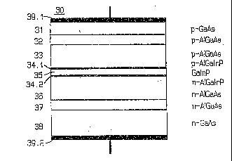
The inventive laser diode 30, schematically shown in Figure 3A, consists of a
double heterostructure with GalnP active layer 35 embedded between a p-doped
upper AlGalnP barrier layer 34.1 and an n-doped lower AlGalnP barrier layer
34.2. The thickness of these barrier layers 34.1 and 34.2 should preferably be
between 0,01 and 0,1 ,um. This layer sequence 34.1, 35, 34.2 is sandwiched
between thick AlGaAs cladding layers 33, 36, the upper cladding layer 33 being
p-doped and the lower claddiny layer 36 being n-doped. Doped AlGaAs
bandgap adaptation layers 32 and 37 are situated on these AlGaAs cladding
layers 33 and 36 as bandgap adaptation to the outer contact layer 31 which
consists of p-doped GaAs on one side and the n-doped GaAs substrate 3B on
the other side. Broad metal contacts 39.1 and 39.2 are deposited on the top and
bottom of the device 30. .
The Al-mole fraction at the contact and substrate side can be slmply graded to
zero, as for example shown in Figure 7B! which in addition helps to eliminate
parasitic barriers. As shown in Figure 4~ the Al (X,~,) fraction in the AlGaAs
cladding layers has to be larger than 0,45 to prevent absorption of the laser light
and to guide the wave efficiently. The upper diagram of Figure 4 shows the
bandgaps of AlGalnP and AiGaAs as functions of the Al fraction (XAI), the middledia~ram shows the wavelength in dependance of the Al fraction (XAI), and the
lower diagram shows the refractive indices of AlGalnP and AlGaAs as functions
of the Al fraction (XAI). The re~ractive indices of AlGalnP are reported in the
article "Refractive Indices of InO,,~GaOs,. xAl~,P Lattice Matched to GaAs", H.
Tanaka et al., Journ. Appl. Phys., Vol. 59. No. 3. Febrl~ary 1~86, pp. 985 - 986.
2û76~
SZ 9-91-017
Exemplary details of the structure shown in Figure 3 are given in Tabla 1.
. . ~
Table 1: Exemplary details of the first embodiment
. .. . . _ _
Layer No . Material DopantDoping Thiclc-
Conc. ness
[cm -3] I ,um]
.... ... _...... ._
p-side contact3g.1Ti/PtlAu 0,3
... __ _ _ ...... _ _
contact layer 31 p-GaAs Zn p = 2 x 101~ 0,1
. __ ..
bandgap 32 p-AlGaAs Zn p = 2 x 10'~ 0,1 x=0,35
adapt. Iayer
_ _ ... . _ .
cladding layer33 p-AlGaAs Zn p = 1 x 10~8 1,5 x=0,7
. ,
barrier layer34.1p-AlGalnP Zn p _ 5 x 10'' 0,05x=0,7
y=0,5
_._ ... __ ~
active layer 35 GalnP none 0,08x=0,5
. .__ ... _ _ . .
barrier layer34.2n-AlGalnP Si n--5 x 10~7 0,05x=0,7
y=0,5
_ . . . . . .
cladding layer36 n-AlGaAs Si n = 1 x 10'a 1,5x=0,5
. _ _ . _ ._ ,
bandgap 37 n-AlGaAs Si n = 1 x 10l8 0,1x=0,35 : ~
adapt. Iayer ~.
~ .__
substrate 38 n-GaAs Si n = 2 x 10'a 350
_ . _ _
n-side contact 39.2 AuGe/Ni/Au 0,3
___
Figure 3 shows a simple structure of a broad contact laser diode 30 with contactsize 50X 1000,um2 . This first embodiment can be simply modified by increasing
20766~
16 SZ 9-91-017
or decreasing the thickness of the iayers, insertlng an unstrained MQW active
structure or a strained MQW active structure replacing the active layer 35
described above. In addltion the inventive structure can be used in a ridye
waveguide laser diode or a mesa stripe laser diode instead of the broad contact
laser diode described above. Graded buffer layers can be employed as known
in the art, replacing the bandgap adaptation layers.
All embodiments herein described are grown on n-doped substrates to simplify
the description and drawings. All shown devices can be modified starting with a
p-doped substrate and successively growing the respective layers, reversely
doped, thereon.
The second embodiment is a AlGalnP/GalnP separate confinement double
heterostructure laser diode. A sketch of the corresponding bandgap diagram is
shown in Figure 6. The undoped GalnP active layer of this embodiment is
embeddsd between two undoped or slightly doped AlGalnP confinement layers.
This active region is sandwiched between thin p- or n-doped AlGalnP barrier
layers and thick p- or n-doped AlGaAs claddings as illustrated in the bandgap
diagram of Figure 6.
The third embodiment based on the inventive structures as shown in Figures 3A,
38, and 6 is illustrated in Figure 7, which shows a schematic cross-section of amulti-quantum well structure and its bandgap cliagram. This third embodiment
is a MQW laser diode 70 its active region consisting of undoped GalnP active
layers 76.1 and 76.2 (quantum wells) separated by a quantum barrier 75.2 and
embedded between waveguide iayers 75.1 and 75.3, these layers consisting of
undoped or slightly p- and n-~oped AlGalnP. This active region is embedded
between an upper p-doped AlGalnP barrier layer 74.1 and a lower n-doped
AlGalnP barrier layer 74.2. The outer layer sequences on both sides of the
device is comparable to the sequence described before. The only difference is
that the bandgap adaptation layers, layers 72 and 78 of the third embodiment,
are graded bandgap layers as shown in Figure 78. By employment of these
graded bandgap layers 72, 78 it is possible to adapt the bandgap of the
doped-AlGaAs claddings 73 and 77 to the cont~ct layer 71 on one side and the
20~0~
17 SZ 9-91-017
substrate 79 on the other side. Exemplary details of the thlrd embodlment are
given in Table 2.
, . _
Table 2: Exemplary details of the ~hird embodlment
._. .. _
Layer No.Material Dopant Doping Thick-
Conc. ness
[cm -3~ [~m]
.
p-side contact 69.1 Ti/Pt/Au 0,25
~-- . _ __ ._ __
contact layer71p-GaAs Zn p -~ 2 x 10~9 0,1
_ ................. _ .. _
graded band- 72p-AllGaAs Zn p = 2 X lot8 0,1 0,l~x
gap layer c0,7
~. . _ .. _ _ ._
cladding layer73p-AlGaAs Zn p = 1 x IQ~8 1,5 x=0,7
.... ~__ m._ .__
barrier layer74.1p-AlGalnP Znp = 5 x 10~7 0,05 x=0,7
y-0,5
_ _ ._ __ _. .. _
waveguide 75.1p-AlGalnP Znp = 2 x 10~7 0,2 x=0,7
layer Y = 0,5
_ __ . . .__ . . ~ . _
quantum well76.1 GalnP none 0,01 x=0,5
... ___ _ __ .... _. :
quantum 75.2AlGalnP none 0,004 x = 0,7
barrier y = 0,5
_ . . _ .
quantum well76.2GalnP none . 0,01 x = 0,7
_ . ... ____ .
waveguide 75.3n-AlGalnP Si n = 2 x 10~7 0,2 x=0,7
layer y = 0,5
. _. . _ _
barrier layer74.2n-AlGalnP Si n = 5 x 10~7 0,05 x=0,7
. _ _ . . y = 0,5
2076~D5
18 SZ 9-91-017
..___
Layer No. Material Dopant Doping Thick-
Conc. ness
Ccm 3] [,um]
, , _ .
cladding layer 77 n-AlGaAs Si n = I x lo~a 1,5 ¦ x=0,7
_. .
graded band- 78 n-AltGaAs Si n = 2 x 10'~ 0,1 0,7>x
gap tayer 20,1
__ _ . -
substrate 79 n-GaAs Si n = 2 x 10¹⁸ 350
__ . _
n-side contact 69.2 AuGe/Ni/Au _ 0,Z5
This embodiment can be easily modified e.g~ by replacing the shown active
region 75.1 - 75.3, 76.1 and 76.2 against other multi-quantum well structures.
Further modifications are illustrated in Figures 8 and 9. In both figures barrier
layers with graded band~aps are shown embedding the quantum well structure.
A parabolic grading of optical confinment layers would be a further modificàtion.
A fourth ernbodiment is illustrated in Figure 10, which shows a cross-sectional
view of an AiGalnP/GalnP laser diode 100 with ridge structure. The active
region 107, shown as cross-hatched layer~ may consist of a double
heterostructure or (multi-) quantum well structure as described before. This
active region 107 is embedded between a thin llpper p-doped AlGalnP barrier
layer 106.1 and a thin lower n-doped AlGalnP barrier layer 106.2. The p-AlGaAs
cladding 104 on top of the upper barrier layer 106.1 forms a ridge, exemplary
shown having vertical sidewalls. A p-doped AlGaAs ~raded bandgap layer 103
and a p-doped GaAs contact layer are deposited on top of this cladding 104.
The sidewalls of the ridge and the thin AlGalnP barrier are covered by a Si3N
insulating layer 105 and the whole structure is co~Jered by a p-metal contact 101
which provides for an electrical contact to the contact layer 102. The whole
layer sequence described above is situated on a substrate (not shown) carrying
an n-doped AlGaAs cladding 108. The ridge structure is formed by etching, e.g
dry-etching (RIE), the p-AlGaAs cladding layer 104. This etch process
automatically stops at the thin barrier layer 106.1 which is another advantage of
2076~5
19 SZ 3-91-017
the inventive structure wlth thin barrier layers. The thickness of the barrler
layers 106.1 and 106.2 may be 0,05 ,um and the thickness h of the ridge
p-AlGaAs layer 104 about 2 ,um. The ridge's width may be 5 ~lm and its length
500 ,um. Exemplary details of the fourth embodiment are given in the following
Table 3.
,
Table 3: Exemplary details of the fourth embodiment
.
Layer No. Material Dopant Doping Thick-
Conc. ness
~cm -3] [,um]
p-side contact 101 Ti/Pt/Au 0!3 -
_ _ _ _
contact layer 102 p-GaAs Zn p = 2 x 10~9 0,1 _
_ __
insul. Iayer 105 Si3N4 0,2
_ . _
graded band- 103 p-AllGaAs Zn p = 2 x 10~8 0,1 0,1<x
gap layer ~0,7
_ _
cladding layer 104 p-AlGaAs Zn p= 1 x 10¹⁸ 1,5 x=0,7
__
barrier layer 106.1 p-AlGalnP Zn p = 5 x 10~7 0,05 x = 0,7
y-0,5
. . _ _ _
actlve reglon 107
__ _ _
barrier layer 106.2 n-AlGalnP Si n = 5 x 10~7 0,Q5 x-û,7
l . y=0,5
__
cladding layer 108 n-AlGaAs Si n = 1 x 10¹⁸ 1,5 x=0,7
_ _
graded band- n-Al~GaAs Si n = 1 x 10~8 0~1 0,7>x
gap layer 20,1
_ _ . _
substrate n-GaAs Si n = 2 x 10~8 350
~: _ _ . . ~
~ ~ n-side contact AuGe/Ni/Au 0,3
..._
:
2~7~
!
SZ 9-91-017
A fifth embodiment is shown in Figure 11. In this figure a longer wavelength
AlGalnAs/GalnAs/lnP laser diode 110 with ridge structure is illustrated. This
structure is comparable to the one shown in Figure 10 but having thin AlSalnAs
barrier layers 116.1 and 116.2 instead of AlGalnP barrier layers. The active layer
117 consists of (Al)GalnAs or GalnAsP and the cladding layers 114 and 118
consist of doped InP. This structure is grown on an InP substrate (not shown),
the inclined surface of the ridge and the upper surface of the barrier layer 116.1
being covered by a Si3NI insulating layer 115. A graded bandgap layer 113, a
GalnAs contact layer 112 and a Ti/Pt/Au contact 111 provides for the upper
contact of the laser diode 110.
The advantages, we observed in applying our invention to the different
embodiments described are listed in the following:
-- the defects generated ~ during MOVPE of conventional structures, as
illusfrated in Figures 1A and 2A, are drastically reduced by replacing the
thick AlGalnP (AlGalnAs) cladding layers against AlGaAs (InP) even for Al
concentrations in AlC~aAs as high as 90 %:
-- lattice matching of the AlGalnP (AlGalnAs) layers is strongly relaxed since
the layer thickness are in general smaller than the critical layer thickness;
-- by intentionally growing strained, compressive or tensile, barrier layers it is
possible to modify the barrier, e.g increasing the barrier height;
by variation of the MOVPE growth temperature during deposition of the
barrier layers, it is possible to grow disordered AlGalnP barriers having
different properties, e.g another bandgap, than ordered AlGalnP barriers.
-- when cgrowing AlGaAs layers with high Al mole fraction by MOVPE, p-dopin~
can be simply accompiished by C-doping adjusting suitable V/ill ratios, an
effect which has not been found yet in AlGalnP. The C is known to be a slow
diffusor and additionally the solubility limit of C in AlGaAs is much higher
2~7~6~
21 SZ 9-91-017
than that of Zn or other acceptors in AlGalnP thus allowing to enhance
substantially the p-doping level;
the acceptor binding energy in AlGaAs For Al is much smaller in comparison
to the one of Zn in AlGalnP, e.g. 40 - 60 meV binding energy for Al mole
fractions > 60 % in comparison to the > 100 meV for Zn in AlGalnP;
the Hall mobility in doped AlQaAs is much higher than that in AlGalnP, e.g.
50--80cm2/Vs in p-doped AlGaAs in comparison to 10 - 2ûcm2/Vs in
AlGalnP;
the last three points allow to reduce the resistivity of the cladding by a factor
up to 100 (~ = n e,u);
the thermal resistance of the AlGaAs cladding layer is, depending on the Al
mole fraction, between 2 and 8 tlmes smaller than that of AlGalnP having a
thermal resistance of about 17Kcm/W. The thermal resistance of AlGalnP is
reported in the article "Thermal Behavior of Visibie AlGalnP/GalnP Ridge
Laser Diodes", O.J~F. Martin et al., IEEE Journ. Quantum Electronics,
submitted 1/1991. By employment of the inventive structure with thick
AlGaAs cladding layers and only very thin barrier layers consisting of
AlGalnP a substantial reduction in the thermal resistance of the visible
AlGalnP lasers can be achieved;
formation of the ridge of ridge waveguide laser diodes either by wet
chemical or dry by dry etching is greatly facilitated since easily conditions
can be selected where the efching stops automatically on the AlGalnP barrier
layer, hence offering ultimate ridge etch depth control. The employment of
etch stop layers is known in the art. In the article "Room-Temperature,
Continuous-Wave Opsration for Mode-Stabilized AlGalnP Visib!e-Light
Semiconductor Laser with a Multiquantum-VVell Active Layer", S. Kawata et
al., Electronics Letters, Vot. 24, No. 24. November 1988, pp. 1489 - 1490, for
example. a QW structure with p-AlGalnP etch stop layer is disclosed.
~ 2076~0~
22 SZ 9-91-017
-- Up to now one had to make a trade-off by chooslny the thickness of
conventional AlGalnP cladding layers. On one hand AlGalnP has a very high
thermal resistance such that thermally optlmized diodes require thin
claddings and on the other hand diodes with thin claddings have a high
astigmatism thus reducing the optical beam quality of the device. An
important advantage of the present invention is that the low thermal
resistance of AlGaAs allows to employ thicker claddings of this material such
that the astigmatism and thermal resistance is lower than in conventional
devices.
To show the advantages of the invention and their influence on the CQD level of
inventive laser diodes, the intensity-current curve of a conventional
AlGalnP/GalnP laser diode, as described in context with Figure 2, and an
intensity-current curve of a diode according to the invention are illustrated inFigure 12. The conventional AlGalnP/GalnP laser diode, its curve being marked
with letter 'A', has a threshold current of about 50 mA and a COD level of
typically 30 mW. The results of the inventive MQW laser diode (curve 'B') with
5 x 500,um2 ridge, described as one of the embodimçnts, has a threshold current
of about 20,5 mA and a COD level about 340 mW. This COD level is about ten
times as high as COD levels of known laser diodes. Both lasers were mounted
junction side-up during the measurements and had uncoated mirrors.
" :