Note: Descriptions are shown in the official language in which they were submitted.
~ 7~
SERRATED ELECTROMAGNETIC ABSORBER
.
BACKGROVND OF THB INVENTION
Electromagnetic wave absorbers and anechoic chambers are in
widespread use throughout the world in making antenna and
reflectivity measurements. Chambers have been designed as
general purpose facilities in order to achieve free space
conditions for measuring the characteristics and properties of
various components and systems, and are employed for a wide
variety of measurements; others have been designed for particular
types of measurements such as antenna impedance, gain, beamwidth,
circularity, cross polarized component levels, antenna patterns,
monostatic and bistatic radar cxoss-section patterns, system
sensitivity, system susceptibility, system compatibility,
effective radiated power, boresite alignment, radome error
tracking error, etc.
Anechoic chambers provide a standard, reproducible
environment which minimizes interfering energy disturbances or
the measurement of a wide variety of electrical and electronic
devices in order to establish or confixm that they meet certain
requirements, such as spurious, harmonic, and noise emissions.
However, conventional absorbers, used to cover ~he walls of
indoor ranges for antenna and scattering measurements, for
example, limit the performance of these ranges. In order to
achieve the desired low reflectivity properties, good absorbers
must provide the following two characteristics:
1. a smooth transition from air into the absorber,
and
2. complete absorption of the wave inside the
,,. , . ~,. , :;
!
absorber.
Presently available absorber materials typically use
homogeneous material cut into either wedges, square pyramids, or
cones. The pyramidal-shaped or cone-shaped elements are arranged
in the chamber so that they project inwardly into the interior
thereof. The absorbers are ormed of a low density material that
exhibits low dielectric properties and which i9 coated or
impregnated with a substance that inherently absorbs microwave
energy. As the microwave energy impinges against the tapered
surfaces of the geometrically shaped absorber, part of the energy
penetrates into the absorber panel while a part of the energy is
reflected. Because of the configuration of ~he absorber panel,
most of the reflected energy is reflected in a direction toward
another absorbing surface of the panel rather than being
reflected back into the interior of the chamber. Pyramidal and
wedge absorbers usually provide better reflectivity performance
at microwave frequencies than do flat or planar layers made from
multi-layers.
Typically, the component to be evaluated in an anechoic
chamber is placed at one end of the chamber facing toward a
position at the opposite end from which a microwave energy signal
can be beamed toward the device under observation. Although the
signal is beamed directly at the device being observed, as the
signal leaves the source o energy illumination the energy waves
tend to diverge to form a signal of constantly expanding cross-
section. The microwave energy absorbing material which lines the
side walls, floor and ceiling of the chamber is intended to
absorb microwave energy which strays too far from the axis of the
, .
. i , .
, ~
:
.
, :
signal beam and impinges against these surfaces of the chamber.
Ideally, all microwave energy impinged against the absorber
material is absorbed so that no wa~e energy is reflected back
into the interior of the chamber to cause interference with the
signal beam and inaccuracies in the measurements being taken.
The achievement of the lowest possible level of reflected
energy in an anechoic chamber depends upon the proper
manipulation of two variables: (a) the characteristics of the
absorbing materials used to cover the internal chamber surfaces;
and (b) the shaping of the chamber to direct residual reflected
energy away from the quiet zone or working volume.
Compact range technology has been significantly improved by
using new reflector designs and pulsed radars with large dynamic
ranges. However/ the scattering from the absorber-coated walls
was found to be a serious limitation on compact range
performance. Accordingly, several studies were made in an effort
to improve absorber performance. Multiple layer wedges were
designed (Figure 1) such that the complex dielectric constant
progressively increased from the outex layer through the inner
layers. This approach gave better reflectivity than commercially
available homogeneous wedge designs because it provided a moxe
gradual transition from air into the absorber. Complete
absorption can be achieved by using internal layers with
sufficiently high loss. However, the multi-layer approach has
the disadvantage that numerous layers are needed to achieve
extremely low reflectivity levels.
,:
,
,, .. .;,. ~:
:~ .
:" ,.
~7~9~
SU~RY OF THE INVENTION
The problems of the prior art have been solved by the
present invention, which provides absorbers designed to provide
better transition from air into the absorber. Absorber means are
provided which applies dual impedance matching to absorb incident
waves. Specifically, serrations, regularly or randomly spaced,
are provided on the surfaces of wedges, pyramids, cones, or other
shaped absorbers with either multiple or uniform dopings to
improve the impedance matching between free space and the
absorber. The serration layer reduces the reflection of the
incident electromagnetic waves from the absorber.
BRIEF DESCRIPTION_ OF THE DRAWINGS
Figure 1 is a perspective view of an absorber having a
multilayer wedge design;
Figure la is an end view of the absorber of Figure l;
Figure 2 is a perspective view of one embodiment of a
serrated absorber in accordance with the present invention;
Figure 2a is a front view of the absorber of Figure 2;
Figure 3 is an oblique view of one embodiment of a serrated
absorber in accordance with the present invention;
Figure 3a is a side view of the absorber of Figure 3;
Figure 4 is an oblique view of one embodiment of a serrated
absorber in accordance with the present invention;
Figure 4a is a top view of the absorber o Figure 4;
Figure 5 is a graphical comparison of the serrated wedge
designs with and without the preferred shift in serrations;
Figure 6 is a graphical comparison of an absorber in
,. . .
'
'
2 ~ Y~
accordance with the present invention and prior art absorbers;
Figure 7 is a graphical comparison of an absorber in
accordance with the present invention and prior a~t absorbexs at
a fixed frequency of 2 GHz;
Figure 8 is a graphical comparison of an absorber in
accordance with the present invention and prior art absorhers at
a fixed fraquency of 6 G~z;
Figure 9 is a graphical comparison of the backscatter of an
absorber in accordance with the prasent invention and prior art
absorbers at a fixed frequency of 2 GHz; and
Figure 10 is a graphical comparison of the backscatter of
an absorber in accordance with the present invention and prior
art absorbers at a ixed frequency of 6 GHz.
DETAlLED DESCRIPTION OF THE INVENTION
In broad terms, the,instant serration concept achieves good
results with dimensions within the bounds such that the total
wedge height is greater than about one wavelength at the lowest
frequency and the height between serrations tips is less than 1/4
wavelength at the lowest frequency.
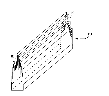
Turning now to Figures 2 and 2a, illustrated is one
embodiment of the present invention in which a wedge shaped
absorber shown generally at 10 is formed of LS-1~ (available
commercially from Emerson & Cuming, Inc. of W. R. Grace 6 Co.-
Conn.) material having a series of sarrations 12 alony its
surface~ The individual wedge has a height of about 2.1
freespace wavelengths (references to free~pace wavelengths are
: i: : :,
: ~ : . : : ::
- : . :
` . , ~ '; '
~:.: : :
:,
. .
.
9 ~ ~
to be construed as freespace wavelengths at the lowest design
frequency) and a width of about 0.7 freespace wavelengths. For
the example found in Figures 2 and 2a, the 2.1 and 0.7 freespace
wavelengths translate to dimensions of 12.6 and 4 inches for the
low frequency design limit of 2.0 GHz. As shown in Figure 2a by
way of illustration, each wedge in the six wedge design is formed
with ten serrations each having a height o 0.68 freespace
wavelengths or 4 inches for the low frequency design limit of 2.0
GHz. That is, the depth of each cut made in the wedge surface
is about 0.7 freespace wavelengths, (corresponding to four inches
at 2.0 GH7); the total height of the wedge with serrations is
about 2.13 freespace wavelengths (corresponding to 12.6 inches
at 2.0 GHz); ~he difference in height between adjacent sexrations
is abou~ 0.2 freespace wavelengths (corresponding to 1.~ inches
at 2.0 GHz), etc. IFigure 2a). Fins 14 are formed by the
serrations, and are shaped so as to taper towards their upper
suxface. Preferably the height of adjacent fins formed by the
serrations on one side of the wedge relative to the other should
be shifted about 0.1 freespace wavelengths, or 0.6 inches ~see
Figure 2a~, which the present inventors have found further
improves the scattering performance of the absorber for the
frequency band of interest~ 2 to 18 GHz. The wedge design
exhibits a good transition over a broad band of frequencies while
achieving sufficient absorption with relatively small heights.
The embodiment illustrated in Figures 2 and 2a was clesigned
for the 2-18 GHz frequency band. Designs based on using
serrations can be made for other fre~uency bands by changing the
physical dimensions of the absorber, and by controlling the raw
9 9 3
material to have the appropriate dielectric properties within the
frequency band of i~s use.
In general, the serrations can be formed by any suitable
means, such as by cutting from the absorber surface, by attaching
fins 14 to the absorber surface, or by molding fins 14 onto the
surface. Preferably the serrations are made by computer aided
cutting in order to maintain the precision needed for this new
shape.
Figures 3 and 3a illustrate a pyramidal-shaped absorber 20
with serrations 12 along its surface (only one face shown with
sarrations). Figures 4 and 4a illustrate à cone-shaped absorber
30 having serrations 12 along its surface.
Figure 5 is a graphical illustration of reflectivity
demonstrating the improved performance achieved by orming the
absorber with serxations such that the resulting fins are shifted
from each other in height by about 0.1 freespace wavelengths or
0.6 inchas, for this case. At almost all frequencies, a wedge
design having sy~metrical serra~ions exhibits a higher specular
reflection coefficient than a wedge having serrations such that
the fins are shifted by a small distance, such as about 0.1
freespace wavelengths or about 0.6 inches for the example
depicted in Figure 5. The graph demonstrates the varsatility of
the instant invention in its capability of arranging the
positions of the serrations depending upon the desired
characteristics for the absorber.
The principle for shifting the heights of the serrations is
to avoid symmetry in the resulting fins. The recommended amount
of shift in the serrations is such to cause the heights of the
:: , , . - , . .. :,
: . :: :,: : ~ :- ,
. ~ , , ;: :
. . :
.
. ' ` ` . .`,'
2~9~
fins on one side of a wedge to lie midway between the heights of
the fins on the other side of the wedge.
The calculated reflectivity performances of several
absorbers are plotted in Figures 6-10, with Figures 6-8 showing
specular scatter and Figures 9 and 10 showing backscatter. From
these data it can be seen that the serrated wedge design having
ten 4-inch serrations (about 0.7 freespace wavelengths) on a
wedge with LS-16 dielectric properties provides much better
performance than conventional WG-8 (available commercially from
Emerson & Cuming, IncO of W. R. Grace ~ Co.-Conn.) wedges, and
indeed, better performance in general than a 4 LS layer design~
The performance of this serrated wedge design in accordance with
the present invention is comparable to a good 8-layer design.
However, the 8-layer design would require careful quality control
in terms of achieving accurate levels of doping for each layer,
whereas the doping level for the serrated wedge design i5 no~
critical. In addition, the multi-layer design rqquire~ adhesive
between layers, whereas the instant serrated design can be cut
from a single block of uniformly doped foam.
The use of the absorber in accordance with the present
invention to cover the surfaces;of indoor ranges, for example,
results in very high absorption of electromagnetic signals,
thereby significantly improving the performance of the ranges.
In addition, smaller ranges can be constructed having
efficiencies that could only previously be achieved by larger
ranges. Existing ranges can be retrofitted with thi~ absorber
as well.
The serrations can be applied to any absorber with either
3 L~ 3
multiple or uniform doping. Any kind of serrations, regularly
or randomly spaced, can be used on the surfaces of the absorber,
so long as dual impedance matching to absorb incident waves is
achieved. One matching comes from the shaplng of the whole
absorber (i.e., wedges, pyramids, cones, etc.) which may be
inhomogeneous, and the other matching is provided by the shaping
of the absorber surfaces into any form of serration or cutting.
-: ~ ' ' ` ,~ ' :,
. ... .
'' : ~. . ~ ,