Note: Descriptions are shown in the official language in which they were submitted.
2077~36
O91t1497~ PCT/US91/01262
ELECTROLESSLY DEPOSITED METAL HOLOGRAMS
Disclosed herein are holograms comprising a
relief-patterned metal surface electrolessly deposited
to conform to a relief-patterned polymeric substrate.
Also disclosed are methods for producing electrolessly
deposited metal holograms.
BACKGROUND OF THE INVENTION
Holograms and other types of diffraction
gratings comprising reflective metal surface on a
relief-patterned substrate are commonly used for
decorative packaging, artistic images and security
devices, e.g. on credit cards, currency and other
official documentsu Such holograms can be prepared by
a variety of methods such as embossing deformable
metal foil laminates with a holographic image stamp.
Due to the resilience of laminate components, such
embossed holograms tend to be of poor quality
especially when subjected to elevated temperatures.
An alternative method is disclosed by
D'Amato et al. in European Patent Publication 0 338
378 where a holographic polymeric substrate is formed
by casting and curing a polymer precursor in contact
with a holographic relief-patterned mold to form a
polymeric substrate with a holographic relief-
patterned surface; a metal reflective surface is then
deposited on the relief-patterned surface, e.g. by
vapor deposition techniques. The resulting relief-
patterned metal surface serves to reflect incidentlight into a reconstructed image of the hologram. A
disadvantage of such metal deposition is the
requirement to conduct such metal deposition in a
vacuum environment and to mask areas where metal
deposition is not desired especially if the hologram
is mounted on a document.
~.
W091/1497~ 2 0 7 7 ~ 3 ~ PCT/US91/01262 ~
--2--
An object of this invention is to provide
such reflective metal holograms which can be prepared
by metal deposition techniques that do not require
vacuum environments or masking. One method for
depositing metal onto polymeric substrates is
electroless deposition. However, electroless
deposition of metal has some disadvantages which do
not commend it to such hologram preparation. For
instance, many techniques for electroless deposition
of metal onto plastics require etching to achieve a
effective level of adhesion; such etching, e.g. with
strong acids or solvents, can destroy the holographic
relief pattern of the polymeric substrate surface.
Moreover, electroless deposition techniques often
utilize catalytic materials of a size on the order
of magnitude of the holographic relief pattern;
deposition of dispersed particulate catalytic
materials can distort the reproduction of the
holographic relief pattern in the metal coating.
2 O SUMMARY OF THE INVENTION
Despite the disadvantages inherent in many
electroless deposition techniques, this invention
provides a hologram comprising a relief-patterned
metal surface electrolessly-deposited to conform to a
relief-patterned polymeric substrate, whereby light
incident to the surface of said metal opposite to said
polymeric substrate is reflected to provide a
holographic reproduction of a holographic image
inherent in said relief-patterned polymeric substrateO
Such metal surface is provided in a thin, conforming
layer that reproduces the holographic relief-
patterned surface of the polymeric substrate by
electroless deposition techniques.
This invention also provides methods of
preparing electrolessly deposited metal holograms,
e.g. preparing a polymeric substrate having a
holographic relief-patterned surface and electrolessly
:: ,
~ WO91/1497~ 20~7~ PCT/US9l/olt62
depositing a conforming holographic metal reflective
layer on said relief-patterned surface. In a
preferred embodiment a polymeric substrate having a
holographic relief-patterned surface is prepared by
casting and curing polymeric precursor in a
holographic relief-patterned mold. The conforming
holographic metal reflective surface is prepared by
electrolessly depositing metal onto the holographic
relief-patterned surface in a method comprising:
(a) coating a holographic relief-patterned polymeric
substrate surface with a film-forming solution of a
polymer and a Group 8 metal;
(b) drying said film-forming solution to form a
polymeric film essentially conforming to and
reproducing said holographic relief pattern;
(c) heating said polymeric film to provide a catalytic
surface thereon;
(d) applying to said catalytic surface an electroless
depositing metal solution for sufficient time to
electrolessly deposit thereon a metal surface which
essentially conforms to and reproduces said
holographic relief pattern. The electrolessly
deposited metal layer allows light incident to the
holographic reproduced metal surface, which is
opposite to the holographic relief-patterned polymeric
substrate, to be reflected to provide a holographic
reproduction of an holographic image inherent in said
relief patterned polymeric substrate.
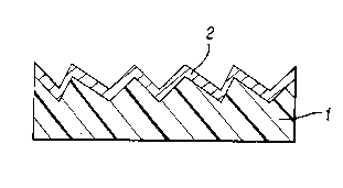
BRIEF_DESCRIPTION OF T~E DRAWING
Figure l is a schematic representation of an
electrolessly deposited metal hologram according to
this invention.
DETAILED DESCRIPTION OF PREFERRED EMBODIMENTS
Referring to Figure l there is illustrated a
polymeric substrate l which can be prepared by molding
a molten thermoplastic, e.g. a high glass temperature
thermoplastic such as a polyimide or polyetherketone,
- : . - : - ~ . - .
Wo91/14979 2 0 7 7 ~ ~ ~ PCT/US91/01~62 ~
in a mold having a holographic relief pattern on its
surface. Preferably, such polymeric substrate can be
prepared by casting and curing thermoset polymer
precursor, e.g. crosslinkable material such as an
acrylate, urethane or epoxy polymer precursor, in a
mold having a holographic relief pattern. Methods for
preparing such substrates are known in the art and are
disclosed by D'Amato et al. in European Patent
Publication 0 338 378, the specification of which is
incorporated herein by reference.
Conforming to the holographic relief pattern
of the polymeric substrate is an electrolessly
deposited metal layer 2 which provides reflective
surfaces from which incident light can be reflected
into a reconstructed image of the hologram inherent in
the holographic relief pattern. As indicated above
many electroless deposition techniques are inherently
incompatible for use in preparing holographic metal
surfaces. It has been discovered that electroless
deposition techniques such as those disclosed by
Norgan et al. in U.S. Patent 4,9lO,072 and by Vaughn -
in U.S. Application Serial No. 07/454,565, the
specifications of both of which are incorporated
herein by reference, are surprisingly advantageous and
efficacious in the preparation of holographic metal
surfaces. The improved electroless deposition methods
of this invention comprise: (a) coating a holographic
relief-patterned polymeric substrate l with a film-
forming solution, preferably substantially aqueous,
comprising a polymer, e.g. polyvinyl alcohol, and a
Group 8 metal, e.g. a palladium salt; (b) drying said
film-forming solution to form a polymeric film
essentially conforming to and reproducing said
holographic relief pattern; (c) heating said polymeric
film by exposure to a temperature of at least about
200 C to provide a catalytic surface thereon; (d)
applying to said catalytic surface an electroless
.
:,
.
2 0 7 7 ~ 3 o
09~/1497~ PCT/US91/01262
depositing metal solution for a contact time of less
than 20 seconds to electrolessly deposit thereon a
metal surface 2 which essentially conforms to and
reproduces said holographic relief pattern. The
drying and heating can be simultaneously effected.
The contact time for applying said
electroless deposition solution should be sufficient
to electrolessly deposit a metal layer 2 in sufficient
thickness, e.g. at least about 5 nanometers thick, to
provide a mirror like surface and sufficiently thin,
e.g. not more than about 300 nanometers thick so as to
not obscure the underlying holographic image. A
balance of good reproduction of the holographic image
and durability of a mirror like finish is achieved
when the metal layer is between about 10 and 100
nanometers thick. Most preferred metal layers are
about 20 to 60 nanometers thick. Preferred contacts
times are less than 10 seconds, more preferably less
than 5 seconds. The contact time can be effectively
reduced by adjusting the electroless deposition
environment, e.g. by elevating temperatures of the
substrate and the electroless deposition solution for
instance up to about 80 - 90 C.
Useful metals for the electrolessly
deposited layer include nickel, cobalt, copper,
palladium, silver, platinum and gold which can be
applied as a single metal layer or a laminate of metal
layers. The metal layer can be optionally overcoated
with a protective wear layer, e.g of a clear acrylate -
or urethane topcoat which does not interfere with the
transmission of light to and from the metal layer. -
An advantage of the electrolessly deposited
holograms of this invention is the application of
methods of preparation thereof to continuous
processing of web material containing such holograms
including web material comprising holograms of
extended length as on artistic or decorative sheets
-
W09l~l4975 2 0 7 7 ~ 3 ~ PCT/US91/01262 ~
-6-
and web material comprising holograms on selected
areas of the web as on security documents. Such
continuous processes are disclosed in European Patent
Publication 0 338 378 referred to hereinabove. The
electroless deposition methods can be effected by
applying the film forming solution and electrolessly
depositing metal solutions from solution saturated
surfaces in register with a moving web so as to
contact the holographic relief surface of the
polymeric substrate and catalyzed relief surface,
respectively.
The following examples serve to illustrate
certain embodiments and aspects of this invention but
are not intended to imply any limitation of the scope
of the invention.
EXAMPLE
This example illustrates the electroless
deposition of a nickel onto a relief-patterned
polymeric substrate.
A catalytic metal solution was prepared from
0.1 g palladium (II) acetate, 2.0 ml water and 10 ml
acetone. A water soluble polymer solution was
prepared from 0.12 g polyvinylalcohol (12S,000 M.W.,
88 mole % hydrolyzed) and 0.013 g Triton X-100
polyoxyethylene surfactant (Rohm & Haas) and about 6
ml water. The catalytic metal solution, followed by
50 ml of rinse water and 0.25 ml triethylamine, was
mixed with the water soluble polymer solution to
provide a substantially aqueous film forming solution.
A polymeric substrate having a hologram generating
relief-patterned surface was coated by wiping the
surface with a sponge saturated with the film forming
solution. The film forming solution was dried by
holding the dry side of the polymeric substrate in a
220- C air stream for about 10 seconds to provide a
catalytic surface on the hologram generating relief-
patterned surface. The polymeric substrate was placed
.
: . . ~; -,
.
~ ~91/1497~ 2 o 7 ~ i PCT/US91/0l262
on a 95- C surface while the catalytic surface was
covered for about 5 seconds with a solution of
electroless depositing nickel solution (obtained from
MacDermid, Inc. identified as XD7054EN) comprising 6
g/l nickel and 30 g/l sodium hypophosphite monohydrate -
adjusted to pH 5.5 with ammonium hydroxide solution
and maintained at about 80- C. After the 5 second
exposure, the nickel solution was rinsed off with
water providing a reflective holographic nickel
surface.
While specific embodiments have been
described herein, it should be apparent to those
skilled in the art that various modifications thereof
can be made without departing from the true spirit and
scope of the invention. Accordingly, it is intended
that the following claims cover all such modifications
within the full inventive concept.
':
.
. , . :.
. , . - . . . . -. .: . . : . : . .
- . , ~ ' '' ' ,