Note: Descriptions are shown in the official language in which they were submitted.
Wo 92/12596 PCI~US92/00148
- 1- 20780~
DYNAMIC OFF8ET TO INCREASE THE RANGE
OF DIGITIZ~TION OF_VlDEO IM~GE8
TECHNICAL FIELD
s
The invention relates to a real-time
imaging system operating in synchronism with an
object field which has components which are periodic
in time wherein unsynchronous background noise is
subtracted leaving only relevant, synchronous
information in the image. The invention applies to
any -wavelength~ of video imaging, whether it-~~be
infrared (IR), visible, ultraviolet (UV), etc.
BACKGROUND OF T~E INVENTION
Lock-in imaging systems have been utilized
to obtain synchronous components from signals having
steady-state and time-varying components. This
technology has recently been expanded to use in video
signal images.
United States Patent Number 4,878,115,
issued October 31, 1989 and assigned to the assignee
of the subject invention, discloses a vector loc~-in
imaging system wherein a video camera detects emitted
and reflected radiation from the object field and
produces the video signal comprising the series of
pixels representing the frame of the image. ~ne
video signal is digitized and received by a process_r
which in turn synchronously averages the success 1 . 2
frames as in-phase and quadrature images based on :~e
periodicity of the object field to elimir._-e
. ,., . ~ .
.
.
.
.
W092/l~596 PCT/US92/00l~
~ tj 7 ~ 2 -
unsynchronous noise ~rom the image and to display the
image synchronous with the periodicity of the object
field.
The vector lock-in imaging system uses an
infrared or visible video camera coupled to a real-
time i~age processor and a computer workstation to
perform phase-sensitive lock-in detection on all of
the pixels of an image in parallel, thus achieving
the effect of having 512 x 512 lock-in amplifiers.
In that invention the processor multiplies the
incoming video signal by the sine and the cosine of
the reference signal in real time, and averages the
two in separate frame buffers to produce in-phase and
quadrature images.
The basic limitation to that invention and
to a wide variety of high speed video ima~ing systems
is the accuracy to which each pixel of the image is
digitized. Typically, this digitization is carried
out to 8-bit accuracy, i.e., to one part in 256. The
reason for this limitation is the difficultly and
expense of maintaining both high speed and high
accuracy in the single digitization process.
SUMMARY OF THE INVENTION AND ADVANTAGES
The invention is a method and apparatus for
producing images which are synchronous with the
periodicity of an object field utilizing a video
camera for producing a video signal comprising frames
of the image. The method and apparatus implements
the steps of producing a reference signal indicating
the occurrence of synchronous signals representing
.
. .
~ :
:
W092/1~596 PCT/US92/00l48
-- 3
2~78'~ I~);i
the periodicity of the object field, detecting
radiation from the object field, producing a video
signal of the image comprising a series of pixels
representing a frame of the image of the object field
and for producing a timing signal for the pixels of
the frame. Further included is obtaining and
subtracting a time-averaged offset from the video
signal producing a time-varying signal, amplifying
the time-varying signal, and storing the frame of the
time-varying signal in synchronism with the reference
signal.
.. ..
In the more specific design, the digitized
video image is averaged over a period of time
corresponding to a few frames, and the resulting
short-term averaged image is converted to an analog
video image. This analog image is in turn subtracted
pixel by pixel from the incoming video signal to the
digitizer, and the resultant video differential
signal is amplified prior to the 8-bit digitization.
Because of the fact that the resultant video image is
an 8-bit deep digitization of the difference signal,
the dynamic range of the corrected image is greatly
increased.
BRIEF DESCRIPTION OF THE DRAWINGS
Other advantages of the present invention
will be readily appreciated as the same becomes
better understood by reference to the following
detailed description when considered in connection
with the accompanying drawings wherein:
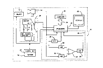
Figure l is a block diagram and schematic
diagram of the subject invention;
Wo 92/12596 PCI/l,lS92/0014~
207~0~5
Figures 2a-b are schematic diagrams of the
processor means;
Figure 3 is a flow chart of the subject
invention; and
Figures 4a-b are illustrations of an
application of the subject invention.
DESCRIPTION OF THE PREFERRED EMBODIMENT
An imaging assembly 10 for producing
dynamically offset images in synchronism with the
periodicitv of an object field 12 is generally shown
at 10 in Figure l. Dynamically offset images of the
synchronous component of the object field 12 are
produced. The assembly lO requires that the portion
of interest of the video signal be periodic, or
quasi-periodic, and be capable of serving as a
reference frequency for synchronization of the
assembly 10. In some cases this periodicity may be
intrinsic, e.g., the combustion process in an engine.
In other cases, the periodicity may be induced by an
external 'stimulus, e.g., a modulated laser beam,
flash lamp, a modulated electromagnetic field, or
modulated electric currents. The assembly 10
achieves, in parallel, and in real time, the effect
of lock-in signal averaging for each of the pixels
produced by the video camera, and at the same time
increases the dynamic range of the resultant
synchronous image through the use of an offset.
Thus, an advantage over prior art imaging syste~s is
the resultant improvement in sensitivity without 'he
relinquishing of the advantage of real-time imac ng
offered by prior art assemblies.
. . ~ . . . - - .
~ .
-
.
;: : :' - -'' ~. .
W092/12596 PCT/US92/~1~
207800'~
-- 5 --
The object field 12 to be imaged may be
comprised of any field which is capable of generating
its own periodic radiation or generating radiation in
response to being externally, periodically
stimulated. Examples of such applicability include:
synchronous thermal wave imaging for nondestructive
evaluation in manufacturing processes; synchronous
detection of fluorescence resulting from modulated
ultraviolet light used as an external stimulus
useful, for example, in the examination of objects of
art, chemical processing, synchronous detection of
~ holographic ~images -with periodic mechanical
vibration, modulated thermoreflectance, etc.
The assembly 10 includes camera means 14
for detecting radiation from an object field 12
providing video and sync timing information which may
be in the form of separate signals or may be in the
form of composite video signals in which the video
and sync timing signals are combined into one
composite video signal. These signals comprise
electrically the image of the object field 12 and
include timing and phase information of each frame of
the imags. The video signal comprises passive and
active radiation. The passive radiation is that
which occurs naturally, such as reflected radiation
or the object's own emitted radiation. The active
radiation is that resulting from external periodic
irradiation of the object field 12 or that radiation
internally generated by the object field 12. .
conventional television camera, infrared viaeo
camera, CID camera, or other camera 14 may be used ~o
obtain the image in the form of pixels accumulated ~o
produce a frame. In this embodiment, the camera `;
. . ~ -
W092/t2596 PCT/US92/00148
produces a composite video signal wherein each pixel
of a frame of the image is serially transmitted, and
therefore the frames are serially transmitted. The
composite video signal is a continuous signal
interrupted after each frame. The camera 14
repeatedly forms an image of the object field 12 and
continuously produces the composite video signal
comprising the pixels formlng the image. The pixels
forming one image constitute a frame and the
composite video signal transmits images, frame after
frame. The frame is comprised of lines of pixels.
In effect, the assembly 10 increases the number of
lock-in channels to that of the number of pixels in
the video image, namely 262,144 in the preferred
embodiment. Typically, 25 or 30 frames/second are
obtained by the camera 14. The timing and phase
information enables a processor means 16 to derive
detailed information about the timing of each pixel
of the image. This provides the mechanism for
acquiring digital images in synchronism with the
periodicity of the object field 12, as subsequently
described.
The assembly includes offset means 18 for
receiving the video signal and subtracting a ti~e-
averaged offset therefrom to produce a data signal
containing substantially only time-varying
information of the image of the object field. In
general, the offset means 18 eliminates the dc an~
slowly varying background signal from the video
signal so that during the digitization step, the
digital resolution of the time-varying data is
increased during the digitization step. Withou. he
offset means 18, the video signal which is digi'i-ed
.
.
.
WO92/12596 PCT~US92/00l4B
- 7 - 2 ~ ~ 8 ~ ~ ~
comprises the dc signal as the major portion of the
video signal. Therefore, the time-varying data would
be limited in dynamic range if the offset was not
included because it represents a small percentage of
the total video signal.
The assembly 10 includes processor means 16
for receiving the video signal, accumulating a frame
of the image and averaging the frame with subsequent
frames producing an image signal representative of
the averaged frame image of the time~varying
information~ synchronous with the periodicity of the
object field 12. The processor means 16 obtains a
sync timing signal from the composite video signal
1~ produced by the camera 14 representing time and phase
information of each frame and separately receives a
reference signal representing the periodic external
stimulation or internally produced periodicity of the
object field 12, as will be described subsequently.
Based upon the phase relationship between the timing
signal and reference signal, the processor means 16
obtains the in-phase image of the object fisld 12, in
a fashion similar to that of the aforementioned
patent. The processor means 16 may be comprised of
2~ off-the-shelf components, as will be described
subsequently. The processor means 16 acts as the
lock-in device for each pixel of a frame of the
entire image. It should be understood that the
quadrature image may be obtained as in the
aforementioned patent.
:': , ,. : . ' '
. .
~ . ~
-- .
,
WO92/12~96 PCT/US92/00l48
2 0 78 ~ 8 -
The assembly 10 includes display means 22
for receiving the analog display signal and for
displaying the synchronous images of the object field
12. Any display or CRT terminal capable of graphics
display may be used.
The preferred embodiment of the subject
invention utilizes an object field 12 which is
externally periodically stimulated at the reference
frequency, or an object field 12 which internally
produces periodicity of the reference signal.
~ Stimulus control-means -28 is included for externally
stimulating the object field 12 at the reference
signal frequency. The stimulus control means 28 may
provide the periodicity by modulated laser beam,
flash lamp, modulated electric currents, or any other
means which will produce the requisite periodic or
quasi-periodic radiation. The periodicity may be
synchronized with the camera 14, or the system may
operate asynchronously with the processor means 16
monitoring same. If the periodicity occurs naturally
in the object field lZ, such as in an engine, the
stimulus control means 28 is unnecessary. Instead, a
sensor means 30 senses the periodicity of the object
field 12 to produce the reference signal for the
processor means 16.
In the preferred embodiment, a phase
correlator means 20 provides a sequentially switched
set of four reference signals A, B, C, D by switch 21
which differ in phase incrementally by 90~. Ihe
output of the phase correlator means 20 from switch
21 is used to control the intensifier of the CID
camera means 14. These signals are switched under
.
- ~- '. '- ' ,
WO92t125g6 PCT/US92/001q8
- 9 - 207~a~
the control of the processor means 16 in synchronism
with the switching of image buffers and look up
tables inside the processor means 16. The averaging
of the frames of data is performed by multiplication
and accumulation operations depending on the phase
relationships.
A computer 32 is connected with the
processor means 16 for receiving the final image and
10 performing post-processing as described in the ~ -
aforementioned patent, incorporated by reference
~herein. The computer 32 and correlator means 20 ~~~
communicates with the processor means 16 via a VME
bus 34.
--
The offset means 18 is specifically
illustrated in Figure 1, and the processor means 16
is more specifically illustrated in Figures 2a-b.
~0 The lock-in detection is carried out in two
channels 35, 36,of the processor means 16. The first
channel 35 establishes the dynamically changing
offset reference image and the second channel 36
performs the in-phase lock-in operation. This is
accomplished by merging the dynamically offset video
signal with the sine of the phase of the reference
signal frequency, and accumulating the results in the
processor means 16. The sine function of the
reference signal may be approximated, for example ~y
a square wave of the same phase relationship.
Both channels 35, 36 are physically
configured the same, except fewer functions ~e
performed in the first channel 35. Both channe7s
.:
- , -
., . ~ . . ::
,:
.
- , . :.,- -
Wo 92tl2596 PCI/US92/00148
2~78~ o
include: sync strlpper 76, 77 for deriving the
master timing signal, gain and offset control 24, 25
for adjusting the gain and offset of the video
signal, analog-to-digital converter 42, 58 for
digitizing the video signal into 8-bits per pixel,
input LUT (look-up table) 26, 27 and operand
transform LUT 73, 74 for obtaining an operand from
the LUT, arithmetic logic unit tALU) 44, 72 for
performir.g the operation with the operand on the
digitized data, clipper 79, 80 and shifter 81, 82,
image buffer 62, 63, output LUT 89,90, and digital-
to-analog~converter 48, 92. The image buffer 62, 63
comprises high and low byte 8-bit buffers 83, 85, ~,
86 and an 8-bit output buffer 87, 88.
The first channel 35 of the processor means
~ 16 utilizes the sync stripper 76, gain and offset
; control 24 and offset digitization means 42 for
receiving and digitizing the video signal to produce
a digital video signal. The offset digitization
means 42 is an 8-bit analog-to-digital converter.
The first channel 35 utilizes the ALU 44 for
receiving and averaging subsequent frames of the
digital signal to establish a dynamically varying
digital reference image. The 16-bit ALU 44 performs
an average of the newly acquired frame from with the
previously acquired and stored frames thereby
establishing a short-term running average frame. The
short term averaged dc image is stored in the 16-bi.
dc buffer 62. The 8 bit D/A 48 converts the sh^rt
term averaged image from buffer 62 to an analog video
offset output signal. The D/A 48 may be a separ~.;e
component apart from the processor means 16.
' `. ' ~ ~
. .
WO 92/12596 PCI-/US92/00148
- 11 - 20'7~
The offset means 18 includes an offset
amplifier 50 for amplifying the analog video offset
signal and a second video amplifier 52 for amplifying
the video signal from the camera 14. The offset
means 18 also includes subtracting means 54 for
subtracting the amplified analog video offset signal
from the amplified camera video signal to produce a
low level video difference signal. The video
difference signal is principally composed of the
informatlon from the time-varying portion of the
object field 12. Data amplifier means 56 amplifies
the video- difference -signal for producing an
amplified offset data signal which is transmltted to
the processor means 16 for input into the second
channel 36. The amplifiers 50, 52, 56 and
subtracting means 54 may be comprised of operational
amplifiers configured as such, as commonly known in
the art.
The second channel 36 of the processor
means 16 utilizes the sync stripper 77, gain and
offset control 25, and image digitizer means 58 for
converting the amplified offset data signal into a
digital image signal. The digitizer means 58 may be
an 8-bit analog-to-digital converter. The image
digitizer means 58 receives and conuerts the analog
offcet data signal from the offset means 18 into the
digital video signal wherein the coding represents
the intensity of each pixel of the image. In the
preferred embodiment, the digital video signal is
comprised of an eight bit binary code signal Der
pixel. In other words, the image digitizer means 50
converts the` serially received analog pi~:el
information and converts each pixel of information
!
W o 92/12596 P(~r/US92/00148
2~78~ 12 -
into the eight bit binary code. ~ecause the final
video image is an 8-bit digitization of the amplified
difference, the dynamic range of the corrected image
is greatly increased. The input LUT 27, operand
transform LUT 74 and ALU 72 perform the in-phase
imaging to process frames of images in-phase with the
reference signal. The in-phase buffer means 63
stores the averaged in-phase image portion. In the
preferred embodiment, the in-phase image buffer 63
is 512 x 512 x 16 blts deep. The imaging means 60
utilizing means 7~, 72, 80, and 82 is as in the
- aforementioned patent.~~
When a predetermined number of frames have
been accumulated by the processor means 16, the
results are normalized and displayed by the display
; means 22 as in-phase images, analogous to the way a
vector analyzer produces in-phase components by
accumulating a single signal for a period of time.
The advantage of parallel processing thereby gained
i5 approximately a quarter of a million.
The preferred embodiment of the processor
means 16 utilizes periodic illumination for the
external stimulus of the object field 12. The camera
means 14 is a commercial CID camera with a gated
intensifier, such as manufactured by ITT. The
digitizers 42, 58 digitize the video signal at 10 .MHz
into an 8-bit digitized video signal.
As indicated in Figure 2a-b, the digitizers
42, 58 reside on boards 66, 66' and the processor
means 16 consists of at least four more boards 68,
70, 68', 70' residing on the bus 34. The boards 56,
WO92/12596 PCT/US92/00l48
2~78~
- 13 -
68, 70, 66', 68', 70' are manufactured by Datacube,
Inc. The display means 22 and computer means 32 are
implemented by the Sun 3/160C Color Workstation. The
pixel timing signals are sent from the first board 66
to all the boards 68, 70, 66', 68', 70' on a sixteen
conductor flat cable 34 in a daisy chain. The
functions of the boards 66, 68, 70, 66', 68', 70' are
implemented by software which follows the flow chart
in Figure 3. The two boards 68', 70' establish the
lock-in operations. The board 68' comprises the in-
phase imaging means 60 and the board 70' comprises
~ the buffer means 63~; ~~The imaging means 60 performs --
the functions or multiplying and accumulating the
digitized video images in the correct sequence
according to the phase information they receive from
the bus 34 and is implemented by the ALU (arithmetic
logic unit) 72. During each frame, a sixteen bit
video data stream is read from the in-phase buffer
means 63 and is merged with the eight bit data from
the digitizer means 58 in the ALU 72 using the
multiply and accumulate operation. -
::;
The imaging means 60 processes the in-phase
portion of the video data and stores it in the in-
2~ phase buffer means 63. The imaging means 60
accumulates the digitized video signal in the in-
phase buffer means 63. The computer means 32 sends
commands to the imaging means 60 in the form of a
control program to operate the processor means as
stated above and transmit control signals to initiate
operation thereof. The processor means receives the
phase information on the bus and points to the
position in the LUT identifying the appropriate phase
of the sine wave. The LUT effects the multiplication
-~:
~, :
WO92t125~6 PCT/US92/001~
~ ~ 7 ~ 14 -
by producing the sine value and transmits the signal
to the ALU 72. For each pixel the above process
occurs. All the sine values are stored in memory of
the LUT 74. The sine values utilized may be as in
the aforementioned patent. The ALU 72 performs the
multiplication and averages same with the buffer 63.
The processing boards 68, 68' are capable
of multiplying, accumulating and shifting image data
in a pipeline fashion with a lOMHz throughput. Each
memory input is a read-and-modify operation, in order
to allow -accumulation of the data corresponding to
each pixel in the same memory location. The pipe-
line delay is compensated for by using a pan
1~ operation (an increment of the horizontal base
register by a count equal to the pipe-line delay at
the pixel rate) at the beginning of each vertical
trace. The controlling program resides in the Sun
workstation 22, 32. All the image processing boards --
66, 68, 70, 66', 68', 70 reside on a VME bus 34 and
are housed in a separate card cage which is connected
to the workstation's VME bus 34 by bus extension
boards. All real-time image processing is handled by
the Datacube boards 66, 68, 70, 66', 68', 70.
More specifically, in the operation of the
processor 16, the first board 66 receives the input
RS-170 analog video signal and a sync stripper 76
derives the master timing signal to synchronize all
the boards 66, 68, 70, 66', 68', 70' thereto. The
video signal is sent to the digitizer 42 comprlsi~g
8-bit A/D (analog to digital) converter. The
resulting digitized video signal is a 10 MHz s.~-a-
of sequential data which is sent to the digital t~
: . :
.
.
.
WO92/1~596 PCT/US92/00148
- 15 - 207~0~
analog converter 48. This offset signal is sent to
the offset means 18. The offset means 18 produces
the amplified offset data signal. The computer means
32 produces a programmed set of commands for the
boards 66, 68, 70, 66', 68', 70'. The commands cause
the data signal to be transformed by the LUT 74 in
accordance with the phase relationship from the
stimulus means 28 or sensor means 30. The processing
board 68' receives the phase information, processes
the data, and puts out a 16-bit modified signal from
the operand transform LUT 7~. The signal is combined
with the 16-bit data previously accumulated in the
storage board 70' using the arithmetic logic unit
(ALU) 72, clipper 80 and shifter 82. The signal .rom
the ALU 72 is sent back to the buffer 63 replacing
the previously accumulated data, and the entire
process is repeated until an appropriate number of
averages have been carried out. The buffer 63 is
capable of storing three (512 x 512 x 8-bit) frames
o.f digital video information. The 16-bit image data
are stored using two 8-bit image buffers 84, 86 (high
byte and low byte). The processing means 16 can
perform temporal and spatial filtering, ir.,age
merging, image subtraction, and addition, and/or
2~ other simple arithmetic operations in real time. ~n
output buffer 88 converts the 16-bit stored image to
8-bits, which a D/A converter 92 converts to analog.
The image data that are transferred to ;he
Color Workstation 22, 32 are in the 8-bit forr.. ~.
These data are obtained from the 16-bit image data ~i
selecting an 8-bit image window with Cpt.-.~
contrast, but without overflow of the data. he
image is displayed with a color map software syste-..
WO92/1~s6 PCT/US92/0014
2 07 8 0~5 - 16 -
It is to be understood that the invention
is not limited to the specific application of visible
imaging, but the embodiment is an example of tAe
assembly's capabilities.
The invention also includes a method for
producing an image of the synchronous component cf an
object field. The method for producing images
synchronous -~ith the periodicity of an object fleld
utilizes a video camera for producing a video slgnal
comprising frames of the image. A reference signal
~ is produced indicating the occurrence of a
sync~ronous pulse representing the periodicity of the
object field. Radiation is detected from the object
l~ field producing a video signal of the ir,age
comprising a series of pixels representing a frame of
the image of the object field and for producing a
timing signal for the pixels of the frame. A
dynamically averaged offset image is obtained and
subtracted from the video signal, and amplifie~
producing an amplified difference signal. The fra~e
of the amplified difference signal is store~ in
synchronism with the reference signal. The s~ored
frame is averaged with subsequently received fr~es
2~ having pixels synchronous with the reference signal
producing a lock-in image with enhanced dyna-.ic
range.
The method includes digitizing the vi~e-
signal, averaging over a period of time correspor.-.ing
to a few frames to form a short-term averaged (acJ
image, converting the digital dc signal to an an.~^g
offset image signal, subtracting the analog ^.~
image signal from the video signal to produce a -.~a
:: :
~ ' ~
WO9~ 5g6 PCT/US92~0014X
- 17 - 2~7~0~ .
signal containing substantially only the synchronous
periodic information of the object field, amplifying
and digitizing the data signal producing a digital
data signal, receiving the timing signal and the
reference signal to produce synchronizing signals,
and transmitting multiply and accumulate commands
using the sine factor for the storing and averaging
prior to the reception of subsequent frames. The
method further includes storing the phase
relationship of the timing signal with corresponding
cosine multiplier factors, the multiply command
~ including the multipiier factor for each pixel, and
averaging successive frames of the object field in-
phase and/or in cuadrature with the reference signal.
Therefore, the subject invention provides a
video camera combined with a video image processor to
simulate a large number of lock-in analyzers when the
object is illuminated or stimulated with the signal
synchronized with the reference signal of the loc~.-in
detection. Furthermore, the subject invention
suppresses the non-synchronous portion of the oblect
field by means of a dynamic offset derived by
performing a short-term average of the video signal.
2~ The resulting information of each pixel of the
offset image is handled as if it were being processed
simultaneously by its own lock-in analyzer, in
synchronism with the periodic portion of the image.
As an example, Figure 4a shc:.s
schematically a pattern of laser light on a scree-
In this pattern there is a large triangle 94 which
has a constant intensity, and a smaller triangle '~
which has an intensity which has both a ste~-~
~, . , ., ,........ , . :
- , ~ -.
W092/l2s9~ PCT/US92/00148
- 18 -
2078~
intensity equal to that of the large triangle and a
superimposed periodic intensity which is varying at
a frequency of 1 M~z and which is 2000 times smaller
than the steady component. Figure 4b is a
5 representation of the dynamically offset lock-in
image 98 obtained wlth the subject invention. This
corresponds to obtaining an ll-bit sensitivity with
the use of an 8-bit digiti~er. Therefore, the
dynamic range has been increased by 3 bits in this
example.
The -invention has been described in an
illustratlve manner, and it is to be understood that
the terminology which has been used is intended to
be in the nature of words of description rather than
of limitation.
Obviously, many modifications and
variations of the present invention are possible in
light of the above teachings. It is, therefore, to
be understood that within the scope of the appended
claims wherein reference numerals are merely for
convenience and are not to be in any way limiting,
the invention may be practiced otherwise than as
specifically described.
:, - ' , '' '.:' ;
. . .